DOI:
10.1039/C9RA08743E
(Paper)
RSC Adv., 2019,
9, 41368-41382
Insight into the PEC and interfacial charge transfer kinetics at the Mo doped BiVO4 photoanodes†
Received
24th October 2019
, Accepted 5th December 2019
First published on 16th December 2019
Abstract
BiVO4 is a promising photoanode material for the photoelectrochemical (PEC) oxidation of water; however, its poor charge transfer, transport, and slow surface catalytic activity limit the expected theoretical efficiency. Herein, we have investigated the effect of Mo doping on SnO2 buffer layer coated BiVO4 for PEC water splitting. SnO2 and Mo doped BiVO4 layers are coated with layer by layer deposition through a precursor solution based spin coating technique followed by annealing. At 5% doping of Mo, the sample (SBM5) shows a maximum current density of 1.65 mA cm−2 at 1.64 V vs. RHEl in 0.1 M phosphate buffer solution under AM 1.5 G solar simulator, which is about 154% improvement over the sample without Mo (SBM0). The significant improvement in the photocurrent upon Mo doping is due to the improvement of various bulk and interfacial properties in the materials as measured by UV-vis spectroscopy, electrochemical impedance spectroscopy (EIS), Mott–Schottky analysis, and open-circuit photovoltage (OCPV). The charge transfer kinetics at the BiVO4/electrolyte interface are investigated to simulate the oxygen evolution process in photoelectrochemical water oxidation in the feedback mode of scanning electrochemical microscopy (SECM) using 2 mM [Fe(CN)6]3− as the redox couple. SECM investigation reveals a significant improvement in effective hole transfer rate constant from 2.18 cm s−1 to 7.56 cm s−1 for the hole transfer reaction from the valence band of BiVO4 to [Fe(CN)6]4− to oxidize into [Fe(CN)6]3− with the Mo doping in BiVO4. Results suggest that Mo6+ doping facilitates the hole transfer and suppresses the back reaction. The synergistic effect of fast forward and backward conversion of Mo6+ to Mo5+ expected to facilitate the V5+ to V4+ which has an important step to improve the photocurrent.
Introduction
Photoelectrochemical (PEC) splitting of water is one of the most promising methods for simultaneous conversion of hydrogen from water using solar energy as a sustainable and clean energy source and zero carbon footprint; the process has inherently high power and energy densities.1–5 PEC water splitting consists of a photoanode and photocathode on which an oxygen evolution reaction (OER) and a hydrogen evolution reaction (HER) respectively are taking place. The overall water splitting reaction, however, is limited by the sluggish OER kinetics; therefore, it is important to develop efficient photoanodes for the improvement in the overall water splitting process. Some of the important materials under continued investigation as photoanode materials for the OER are TiO2, α-Fe2O3, WO3 and BiVO4.6–14 Among these materials, BiVO4 is the most researched photoanode due to its suitable band position, bandgap and high theoretical efficiency (∼7.5 mA cm−2) and high solar to hydrogen (STH) conversion efficiency (∼9%).15–18 However, the slow surface catalytic activity, short hole diffusion length, fast electron–hole recombination are major challenges with the BiVO4.6,19–22 To overcome these challenges, a number of the strategies have been widely investigated such as; nanostructure control,23–26 band engineering,17,27–34 heteroatom doping,35–41 generation of oxygen vacancy22,42–44 and the oxygen evolution catalyst (OEC) incorporation.18,45–53 SnO2 has been used for the heterojunction formation in the BiVO4 system which suppresses the back electron–hole recombination process.17 Additionally, the SnO2 underneath of BiVO4 blocks the surface state of the ITO/FTO. These modifications improve the injection of the photogenerated holes to the electrode–electrolyte interface. During OER at the photoanode surface, photogenerated holes are expected to react with the OH− to form OH˙ radical intermediate, which is converted to O2 and very small part of them dimerize to H2O2 or OH−. Some of the OH˙ intermediate diffuse out into the electrolyte. The charge transfer kinetics at the electrode–electrolyte interface is in the range of nanosecond, which is very difficult to investigate by the conventional electrochemical method. Electrochemical impedance spectroscopy (EIS)54 and the transient absorption spectroscopy (TAS)21 are two important techniques implied to investigate the PEC processes and generate important parameters like photo-induced carrier lifetime and diffusion length.
Scanning electrochemical microscopy (SECM) is a powerful technique to investigate the charge transfer kinetics for in situ measurements at the solid–liquid and liquid–liquid interfaces.55–57 SECM is decisively applied for the investigation of the mechanism of interfacial charge transfer processes in OER, HER, oxygen reduction reaction (ORR) and hydrogen oxidation reaction (HOR) on the Pt, Pd, Au Hg, and the other electrodes.56,58,59 Interfacial charge transfer kinetics at the semiconductor–electrolyte interface has been investigated for the photo-induced charge mediated reactions.60 Bard group has demonstrated the detection, quantification, and evolution of decay kinetics of the photogenerated hydroxyl radicals in the PEC on the semiconductor interface.61,62 Surface interrogation SECM (SI-SECM) technique has been utilized to quantify photogenerated hydroxyl radicals (ads) and dimerization of the photogenerated radicals at the photoanode.
Considering the shortcoming of BiVO4, present investigation is aimed to improve the catalytic efficiency by developing the BiVO4 photoanodes with SnO2 as interlayer, BiVO4 was doped with Mo to further improvement of the catalytic activity. The SnO2 coating over the ITO plate was carried out for suppressing the charge recombination process through the generation of heterojunction of SnO2 and BiVO4. The optical, chemical, and electronic properties of the materials have been investigated to understand the improvement in the PEC efficiency on Mo doping. The improvements in the photocurrent on Mo doping are analyzed based on the relative improvements in the bulk and surface properties as measured by the EIS and Mott–Schottky analysis. The decrease in the charge transfer resistance (Rct) shows the improvements in the bulk property of the BiVO4. The increase in the capacitance upon the Mo doping suggests better activity at the electrode–electrolyte interface due to the enhancement of the active surface sites, which leads to the enhancement in the PEC efficiency.20 Strong correlation among the optical property of the material, the open circuit photovoltage (OCPV), and onset potential was discussed in relation with the improvement in the PEC efficiency on Mo doping. The increase in the flat band potential and OCPV suggests the improvements in the charge separation upon the Mo doping which resulted in the enhancement in PEC efficiency.63–66 SECM has been applied to investigate the photo-induced interfacial charge transfer kinetics in situ at the electrode–electrolyte interface, the interfacial photo-generated hole transfer kinetics was correlated with the efficiency of PEC process across different catalysts investigated.
Experimental section
Materials
Bismuth(III) nitrate (Bi (NO3)3·5H2O, 98%), ammonium vanadate (NH4VO4, >99%), stannic chloride (SnCl4, 98%), and sodium sulfite (Na2SO3, 98%) were purchased from Sigma Aldrich. Ammonium tetrathiomolybdate ((NH4)2·MoS4, 99.95%) was purchased from Alfa Aesar. Sodium sulphate (Na2SO4), sodium monohydrogen phosphate (Na2HPO4), and sodium dihydrogen phosphate (NaH2PO4) were obtained from Sarabhai M Chemicals. Ethylene glycol and potassium ferricyanide were purchased from SDFCL and used as received.
Fabrication of photoanode
SnO2/BiVO4 heterojunction was prepared by the spin coating technique. In this typical synthesis procedure, SnCl4 (98%, 0.24 mL, 0.2 M) was dissolved in 10 mL of ethylene glycol and sonicated for 20 min and kept for stirring overnight prior to the spin coating. An aliquot of 100 μL as prepared precursor solution of SnO2 was spin-coated on the ITO substrate at 2000 rpm for 1 min, followed by annealing at 250 °C on the hot plate for 5 min. This process was repeated 8 times to get the optimum thickness of SnO2.67 After spin coating; the modified electrodes were annealed at 450 °C in a tube furnace for 2 h at 5 °C per minute heating rate to form crystalline SnO2. After having the SnO2 layer over the ITO substrate, the BiVO4 film was formed on the ITO/SnO2 substrate by metal–organic decomposition method. In this typical synthesis method, Bi(NO3)3·5H2O (0.2 mmol) was dissolved in 5 mL of ethylene glycol–water mixture (8![[thin space (1/6-em)]](https://www.rsc.org/images/entities/char_2009.gif) :2, volume ratio) subsequently NH4VO3 (0.2 mmol) was added slowly, the mixture was sonicated for 30 min and kept on stirring for overnight at room temperature. The above solution was spin-coated over ITO (for control experiments) and ITO/SnO2 substrate at 2000 rpm for 1 min and then annealed at 350 °C for 5 min on the hot plate. The coating was carried out for repeated 8 times to achieve the appropriate thickness for maximum efficiency,67 and after completion of the coating, the samples were heated at 450 °C for 3 h at the heating rate of 5 °C per minute in a tube furnace. Mo doping was achieved by adding ((NH4)2·MoS4, 99.95%) at 1, 3, 5 and 7 atom percentage, resulting in a mixture containing Bi/(V + Mo) = 1:1 to replace V position in the crystal lattice of BiVO4. The photoanodes thus fabricated using without Mo and at 1, 3, 5 and 7 atom percentage of Mo are designated as SBM0, SBM1, SBM3, SBM5, and SBM7 respectively.
:2, volume ratio) subsequently NH4VO3 (0.2 mmol) was added slowly, the mixture was sonicated for 30 min and kept on stirring for overnight at room temperature. The above solution was spin-coated over ITO (for control experiments) and ITO/SnO2 substrate at 2000 rpm for 1 min and then annealed at 350 °C for 5 min on the hot plate. The coating was carried out for repeated 8 times to achieve the appropriate thickness for maximum efficiency,67 and after completion of the coating, the samples were heated at 450 °C for 3 h at the heating rate of 5 °C per minute in a tube furnace. Mo doping was achieved by adding ((NH4)2·MoS4, 99.95%) at 1, 3, 5 and 7 atom percentage, resulting in a mixture containing Bi/(V + Mo) = 1:1 to replace V position in the crystal lattice of BiVO4. The photoanodes thus fabricated using without Mo and at 1, 3, 5 and 7 atom percentage of Mo are designated as SBM0, SBM1, SBM3, SBM5, and SBM7 respectively.
Photoelectrochemical measurements
Photoelectrochemical measurements were performed using the CH Instrument (920 D model) using a three-electrode cell with an Ag/AgCl (3.0 M KCl) reference electrode, glassy carbon rod as counter and modified ITO coated with the catalyst material as the working electrode. 0.5 M Na2SO4 solution in 0.1 M potassium phosphate buffer solution (PBS, pH = 7) was used as electrolyte. All photoelectrochemical studies were carried out using Ag/AgCl (3 M KCl) reference electrode and potentials were converted and reported to reference hydrogen electrode (RHE) using the following eqn (1).| | |
E(RHE) = EAg/AgCl + 0.059pH + E0Ag/AgCl
| (1) |
where, EAg/AgCl is working potential and E0Ag/AgCl is standard potential (i.e. 0.2243 V).
To measure the charge transfer efficiency and the charge transport efficiency, 0.1 M Na2SO3 as hole scavenger was added in the electrolyte. All samples were front-illuminated because of significantly higher photocurrent than that of back illumination. Solar simulator having 1 sunlight fitted with AM 1.5 G filter was used as a light source. The xenon arc lamp is used as a monochromatic light source; power of the monochromatic light is measured by digital power meter from Newport. The photocurrent was measured by linear sweep voltammetry (LSV) technique with 5 mV s−1 scan rate and chopped light voltammetry was recorded. Chronoamperometry was used for the stability test of the photoanode materials. Electrochemical Impedance Spectroscopy (EIS) was used to measure interfacial charge transfer resistance (Rct) at 1.44 V by applying sinusoidal wave of amplitude 10 mV in the frequency range from 105 to 10−1 Hz under 1 sun illumination. Further, the relaxation frequency and time constant of the electrochemical process were measured from EIS data to quantify the efficiency of the photoanode materials. Mott–Schottky experiments were carried out at 100 Hz frequency for the measurements of donor density and flat band potential of photoanode material which inherently affects the PEC activity. Incident photon to current efficiency (IPCE) was measured with the setup similar to that of PEC measurement with monochromatic light from 350 to 650 nm with a 10 nm step. The incident light power was measurement at each wavelength with a calibrated photodiode. SECM study was performed on 920 D bi-potentiostat (CH Instrument) using four electrodes system. SECM Teflon cell was in-house fabricated for holding the substrate at the base with O-ring, reference and counter electrodes. Photoanode materials were used as the substrate, Ag/AgCl (3 M KCl) as a reference and glassy carbon rod as a counter electrode and results are reported in terms of RHE potential. Commercial Pt ultra microelectrode (UME) having RG value of 5 and a diameter 9 μm was used as the probe. Pt microelectrode was polished with a micro polishing cloth with 0.05 μm alumina powder successively and then cleaned in 0.5 M H2SO4 solution for 20 cycles of cyclic voltammetry scans in the potential window of 1.44 V to 0.29 V vs. RHE at the scan rate of 50 mV s−1. Ferricyanide solution of 2 mM concentration was used as a redox couple in 0.1 M PBS of pH 7. The potential of the probe was chosen at 0.64 V in the region of steady diffusion current after recording the CV in 2 mM ferricyanide solution with a scan rate of 50 mV s−1. Samples were illuminated from the front side using the solar simulator as the light source. Probe Approach Curve (PAC) technique was used to record the approach curve to the substrate in dark and also under the illumination of light to measure the kinetic parameter using four electrodes system at different polarization potentials, from the fitting of the probe approach plots the interfacial charge transfer kinetics were obtained. The mapping of photoanodes was carried out by the SECM technique (constant height mode) under the illumination condition to map the catalytic activity of the catalyst substrate.
Characterization of the materials
XRD analysis of the prepared samples was performed by using a Rigaku powder diffractometer (9 kW Rotating Anode) with Cu Kα radiation (λ = 1.5406 A). Raman spectra of photoanodes were recorded by using Lab RAM HR 800 Microlaser Raman system with an Ar+ laser of 516 nm. The morphology of the photoanodes was examined by field emission scanning electron microscopy (FE-SEM, JEOL model JSM-7600F). X-ray photoelectron spectroscopy (XPS, MULTILAB, VG Scientific, Al Kα radiation as monochromator) was used to investigate the binding energy of the components of Mo doped BiVO4 photoanodes.
Result and discussion
Structure analysis by XRD and Raman spectroscopy
SnO2/Mo-doped BiVO4 was as synthesized by sol–gel spin coating method67 are characterized by X-ray diffraction (XRD) technique, results are shown in Fig. 1A. XRD peaks at 2θ values of 18.59°, 28.61°, 30.01° and 34.96° correspond to (101), (112), (004) and (020) planes respectively of monoclinic phase (JCPDS 75-1867) of BiVO4. XRD peaks at 2θ values of 26.48° and 50.46° correspond to (110) and (211) plane confirms the presence of inner layer tetragonal SnO2 (JCPDS card 77-0450). The presence of these two layers indicates the successful formation of heterojunction. Upon an increase in the atomic percentage doping of Mo, a small shift of peak position towards the lower theta value indicates the expansion of crystal lattice. It has been reported that Mo preferentially substitutes V sites, which is a thermodynamically favorable process, as the impurity formation energy of Mo doping in V sites and Bi sites is 0.53 eV and 2.79 eV, respectively.68,69 Moreover, Mo is 6 fold coordinated in MoO3, and V and Bi are having 4 folds and 8 folds coordination, respectively. Thus, when Mo atoms substitute V, all Mo–O bonds are expanded; however Mo atoms still keep the 4-folds coordination of V atoms. It has been reported that Mo doping in BiVO4 causes deviation of the dipole moment of VO43− tetrahedron from zero to non zero dipole moment in the crystal lattice, thus making the crystal more polar. This enhanced dipole moment due to the distorted polyhedron are reported to promote the charge separation on photo-excitation, which would enhance the overall photocatalytic activity.69
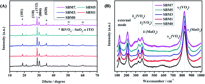 |
| | Fig. 1 (A) XRD patterns of all BiVO4 and Mo doped photoanodes and (B) Raman spectra of all BiVO4 based photoanodes. | |
Raman spectroscopy is used to investigate the crystallization, local structure and electronic properties of the materials. Fig. 1B shows the characteristic Raman bands of the photoanode materials and tabulated in Table 1. The typical Raman bands of BiVO4 are observed at 825.50, 713.80, 367.37 and 329.72 cm−1. The strongest band near 825 cm−1 is assigned to the νs (VO4) (Ag) and weak shoulder like peak at 713.80 cm−1 is assigned to the νas (VO4) (Bg) mode. The Raman band near 367.37 and 329.72 cm−1 are assigned to the δs (VO4) (Bg) and δas (VO4) (Ag) respectively. The external modes (rotational and translational) are at lower frequencies than the internal modes of VO43− units because they involve the heavier VO43− unit and having weaker coupling interactions. The modes at 213.23 cm−1 and 126.58 cm−1 are assigned as rotational and translational modes respectively.70–75 The weak bands at 867.50 cm−1 and 374.70 cm−1 are assigned to the νs (MoO4) and δ (MoO4) respectively. The band corresponds to the νas (MoO4) might be covered with 825.50 cm−1 peak. All these Raman band assignments for the present materials correspond well with the literature reports of similar materials.70–75 It has been observed that there is a blue shift in the most intense peak from 825.50 cm−1 to 829.54 cm−1 in materials from SBM0 to SBM3 then red shifting is observed in SBM5 to SBM7. The change of vibrational frequency of V–O can be explained in terms of metal–oxygen bond length and strength. F. D. Hardcastle et al. have determined the V–O bond length and bond order from Raman stretching frequencies.75 Calculations are made based on the correlation of diatomic approximation which assumes that each metal–oxygen bond vibrates independently in the crystal lattice. The empirical formula used for calculation of bond length is as follows75
| | |
ν (cm−1) = 21349exp(−1.9176R (Å))
| (2) |
where
ν is the Raman stretching frequency for V–O in cm
−1 and
R is the bond length in Å. It can be seen that the V–O bond varies from 1.696 Å to 1.698 Å upon doping of Mo in BiVO
4 lattice; thus a marginal increase in the V–O bond length is observed at the 5% Mo content. The asymmetric stretching also has shown similar behavior to that of the symmetric stretching vibrations, where the V–O bond length is decreased initially on the addition of Mo, with further addition of Mo resulted in the increase in V–O bond length. The increase of the V–O bond causes distortion in the lattice, which has resulted in the shifting of XRD peaks towards lower theta values. However, the shifting is not significant in the modification of the crystal structure.
Table 1 Analysis of Raman spectroscopy of all BiVO4 based photoanodes. All stretching and bending modes of vibrational of BiVO4 are listed here. The bond length of V–O is calculated based on the symmetric stretching of V–O mode
| Catalysts |
νs (V–O) cm−1 |
V–O bond length Å |
νas (V–O) cm−1 |
δs (VO4) cm−1 |
δas (VO4) cm−1 |
Rotational cm−1 |
Translational cm−1 |
νs (MoO4) cm−1 |
δ (MoO4) cm−1 |
| SBM0 |
825.50 |
1.696 |
713.80 |
367.37 |
329.72 |
213.23 |
1286.58 |
— |
— |
| SBM1 |
827.54 |
1.695 |
710.19 |
369.37 |
327.72 |
213.23 |
128.18 |
— |
— |
| SBM3 |
829.54 |
1.694 |
708.19 |
369.37 |
327.72 |
213.23 |
125.04 |
867.50 |
— |
| SBM5 |
823.13 |
1.698 |
715.80 |
366.16 |
330.92 |
212.30 |
125.04 |
867.50 |
374.70 |
| SBM7 |
823.94 |
1.697 |
716.21 |
367.37 |
330.92 |
212.90 |
125.64 |
867.50 |
374.70 |
XPS analysis of the materials
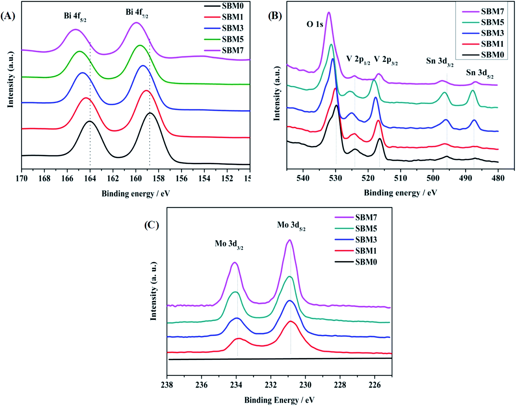
XPS was used to investigate the surface electronic properties of photoanodes. As shown in Fig. 2, XPS spectra confirm the presence of elemental constituents of Bi, V, O, Mo and Sn of deposited films on ITO. Fig. 2A shows the spectra of the Bi 4f core level region. The Bi 4f region is characterized by the presence of the 4f5/2 and 4f7/2 components with a spin–orbit splitting of 5.22 eV. Likewise, V 2p is characterized by the 2p1/2 and 2p3/2 components with spin–orbit spitting of 7.64 eV as shown in Fig. 2B. There are peaks corresponds to the Sn 3d confirm the presence of the inner layer of SnO2 of BiVO4. Doping of Mo with varying concentrations has been carried out in BiVO4, and corresponding XPS spectra are shown in Fig. 2C. Mo 3d is confirmed by the presence of Mo 3d3/2 and Mo 3d5/2 spectra with spin–orbit splitting of 3.06 eV, which confirms the doping of Mo in BiVO4 lattice, which is in accordance with characterization by XRD and Raman measurements. The surface atomic composition of each sample is calculated using Bi 4f7/2, V 2p3/2, Mo 3d5/2 spectral intensities, weighted by atomic sensitivity. The atomic composition is found to be in good agreement with EDS analysis. Further, in addition to the chemical composition of constituent's elements, chemical states are determined from XPS measurements. Fitting of Bi 4f spectra reveals that each spin–orbit split corresponds to the single oxidation state in all samples. The binding energy positions of Bi 4f7/2 and Bi 4f5/2 in BiVO4 are observed at 158.78 eV and 164.0 eV respectively, and the spin–orbit splitting energy of 5.22 eV suggests that Bi is in +3 oxidation state.76–79 The binding energies of V 2p3/2 and V 2p1/2 are 516.41 eV and 524.05 eV, and spin–orbit split energy is 7.64 eV suggests that V is in +5 oxidation state.76–79 All samples exhibit peaks at ∼530 eV for O 1s orbital, which is due to the lattice oxygen. Hydroxyl O 1s peak is also observed near 532 eV suggests the hydroxylated surface of photoanodes, which might enhance the photo-electrocatalysis. Additionally, Mo dopant was characterized by Mo 3d peaks. The binding energies of Mo 3d3/2 and Mo 3d5/2 are 233.94 eV and 230.88 eV, respectively having spin–orbit split energy 3.06 eV confirming Mo is in +6 oxidation state.79,80 The increase of binding energy of all ions (Bi3+, V5+, O2−), in Mo doped BiVO4 is the result of doping of higher electronegative dopant (i.e. Mo6+: 2.16 > V5+: 1.63) (Table 2).81
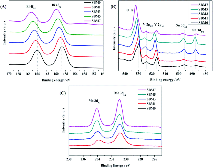 |
| | Fig. 2 XPS spectra of (A) Bi 4f, (B) O 1s, V 2p and Sn 3d and (C) Mo 3d in BiVO4. | |
Table 2 XPS analysis of Bi 4f, O 1s, V 2p and Mo 3d binding energy
| Catalysts |
Bi 4f5/2 eV |
Bi 4f7/2 eV |
O 1s eV |
V 2p1/2 eV |
V 2p3/2 eV |
Mo 3d3/2 eV |
Mo 3d5/2 eV |
| SBM0 |
161.0 |
158.78 |
529.80 |
524.05 |
516.41 |
— |
— |
| SBM1 |
161.34 |
159.07 |
529.94 |
524.21 |
516.84 |
233.94 |
230.87 |
| SBM3 |
164.70 |
159.37 |
530.83 |
525.10 |
517.60 |
233.99 |
230.92 |
| SBM5 |
164.94 |
159.60 |
531.34 |
525.36 |
518.11 |
234.10 |
230.93 |
| SBM7 |
165.27 |
159.26 |
531.96 |
524.21 |
516.71 |
234.10 |
230.90 |
SEM and EDS analysis
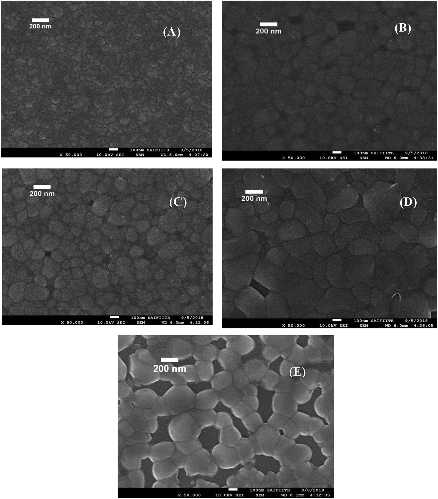
Morphology of photoanode materials was characterized by scanning electron microscopy (SEM). BiVO4 was uniformly coated on ITO/SnO2 as shown in Fig. 3. The materials have shown the granular type of morphology, and the grain size is observed to be increased marginally with Mo doping. Similar observation has been reported in the literature.82–85 On 7% Mo doping, the sample has shown chains of grains with vacant spaces in the matrix. Elemental analysis was carried out by energy dispersive spectroscopy (EDS) as shown in Fig. S1 of the ESI.† In SBM0, the atomic ratio of Bi and V is 1:1 as shown in Table S1 (ESI†). The atomic percentage of Bi, V, O, and Mo was found as these materials were taken during the synthesis procedure. Sn content corresponding to inner layer SnO2 was observed. Further, the thickness of the coating was measured and shown in Fig. S2 (ESI†). The thickness of the combined layers of SnO2 and BiVO4 was found to be around 440 nm.
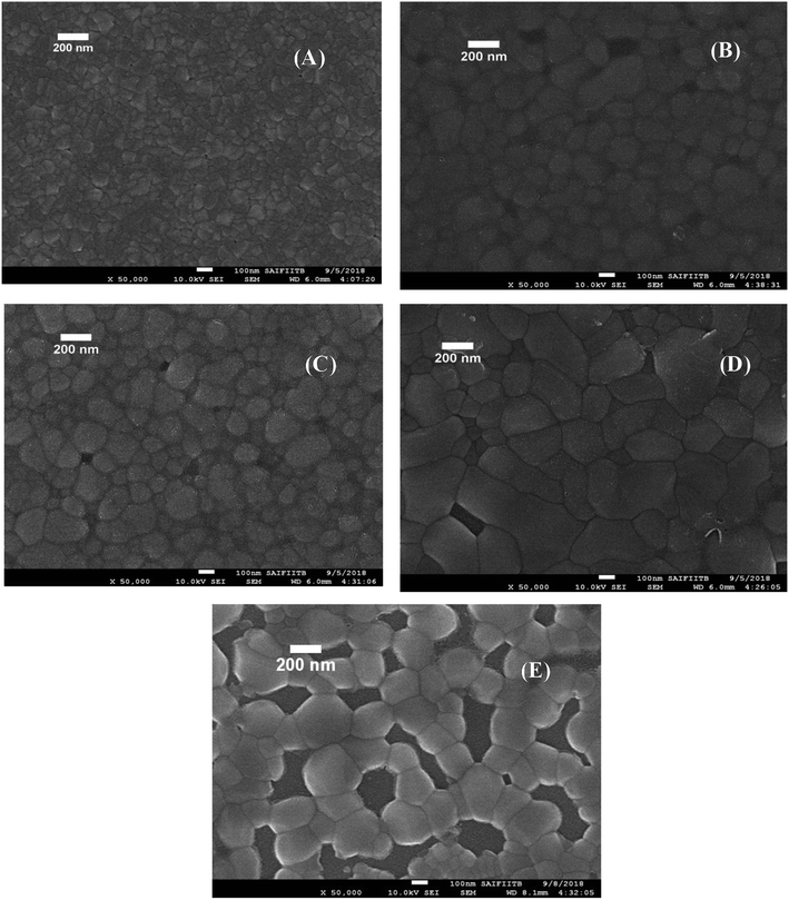 |
| | Fig. 3 FE-SEM images all porous BiVO4 based photoanodes thin films on ITO substrate. (A) SBM0, (B) SBM1, (C) SBM3, (D) SBM5 and (E) SBM7. | |
UV-vis spectral measurements
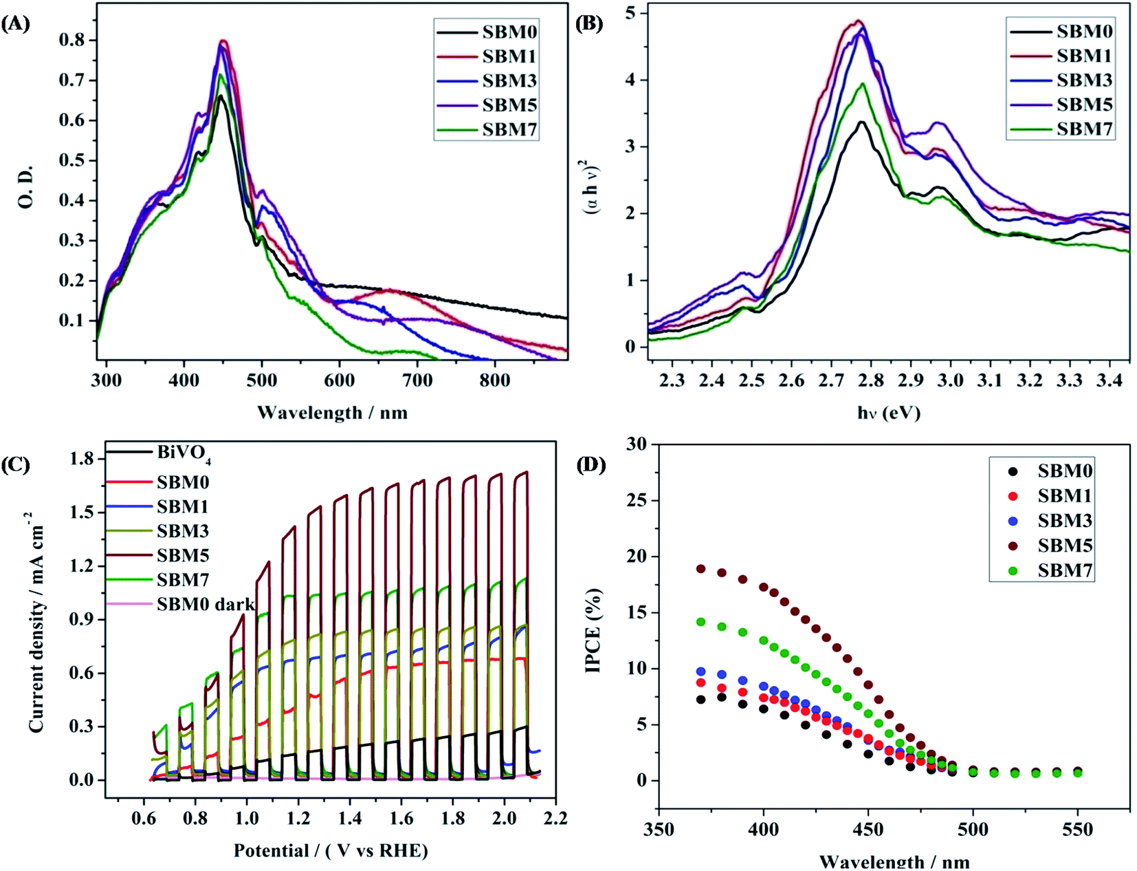
The optical absorption property of a semiconductor reflecting the electronic property of the material is a key factor for determining the photoelectrocatalytic activity. All photoanodes materials are characterized by UV-vis diffuse reflectance spectra of as shown in Fig. 4A. All samples show strong absorption in the visible region, having bandgap absorption edge in the region of 500–550 nm. The most intense absorption peak was observed at 447 nm for BiVO4. The absorption bands correspond to the MoO3 and SnO2 are also observed at 418 nm and 358 nm respectively. A small red shift of absorption edge upon Mo doping is observed. Under the assumption of parabolic band dispersion, the energy dependence of optical transition strength can be explained by Tauc equation86,87Where α is optical absorption coefficient, hν is photon energy, Eg is the bandgap and A is a probability constant. The numerical values of n are 1/2 and 2 for indirect and direct transition, respectively. Thus the nature of the transition can be determined from the linearity of plots of (αhν)1/2 and (αhν)2 vs. hν and bandgap can be determined from the x-axis intercept. Fig. 4B shows the Tauc plot for direct band transition. The bandgap of undoped BiVO4 is obtained as 2.54 eV. Upon Mo doping, the bandgap is found to decrease marginally from 2.54 to 2.50 eV. On Mo substitution on V site, the band structure remained nearly the same as that of undoped BiVO4. The marginal decrease in the bandgap, which means the optical absorption threshold, will not be affected by Mo doping in BiVO4.35,68,69,88 According to the density of state (DOS), Mo 4d states are mainly distributed in the bottom of VB and CB. Mo atoms have more valence electrons than V and Bi atoms. Thus doping of Mo atoms provides the extra electrons, which cause the rise of the Fermi level. Due to such excess electrons from Mo, impurity energy levels will be formed at the bottom of CB or VB, which would generate more electronic levels; this may lead to better catalytic activity on photoexcitation. The formation of impurity level also generates the broadening of the VB and CB.
 |
| | Fig. 4 (A) UV-vis diffuse reflectance spectra and (B) Tauc plot for direct band for calculation of bandgap of all BiVO4 based photoanodes (C) photoelectrochemical performances of the all BiVO4 based photoanodes were measured by chopped light voltammetry in 0.5 M Na2SO4 in 0.1 M PBS buffer solution at scan rate 10 mV s−1 under the 1 sun illuminations. (D) IPCE spectra at 1.0 V vs. Ag/AgCl of all photoanodes. | |
Photoelectrochemical investigation
All PEC experiments were carried out in 0.1 M PBS of pH 7 using 0.5 M Na2SO4 as supporting electrolyte using three electrodes systems in 1 sunlight source using a solar simulator. Photoresponse of photoanode materials was performed by chopped light voltammetry technique, as shown in Fig. 4C. At 1.64 V (vs. RHE) the current densities of 0.65 mA cm−2, 0.73 mA cm−2, 0.84 mA cm−2, 1.65 mA cm−2 and 1.06 mA cm−2 are obtained for SBM0, SBM1, SBM3, SBM5 and SBM7 respectively. The BiVO4 without having the SnO2 interlayer has shown the photocurrent of 0.22 mA cm−2. The results thus indicate significant improvement in the photocurrent response due to the formation of the SnO2 interlayer. The photocurrent is further increased by doping Mo in BiVO4. SBM5 has shown the highest photoelectrocatalytic activity. There is ∼154% improvement in the photocurrent from SBM0 upon 5% Mo doping observed in SBM5.
To understand the photoelectrocatalytic activity of BiVO4 and Mo doped BiVO4, further the incident photon to current efficiency (IPCE) was measured at 1.64 V (vs. RHE) in 0.1 M PBS from 370 nm to 550 nm wavelength range, and the results are shown in Fig. 4D. For IPCE measurements, LSV was recorded for the wavelength ranging from 370 nm to 550 nm, and photocurrents were sampled at 1.64 V, and then IPCE was measured by using the following equation89
| |
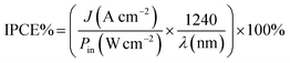 | (4) |
where
J is the photocurrent density,
Pin is the power of incident photon (monochromatic light),
λ is wavelength in nm. The onset wavelength of IPCE is 500 nm, which corresponds to the bandgap of 2.48 eV, supports the bandgap calculation from the Tauc plot. On Mo doping IPCE is increased up to the Mo doping of 5%, thereafter on further doping of Mo, no increment is observed. At 5% Mo doping in sample SBM5, IPCE is observed to be at 17% which is about 166% improvements than that of SBM0 at 400 nm.
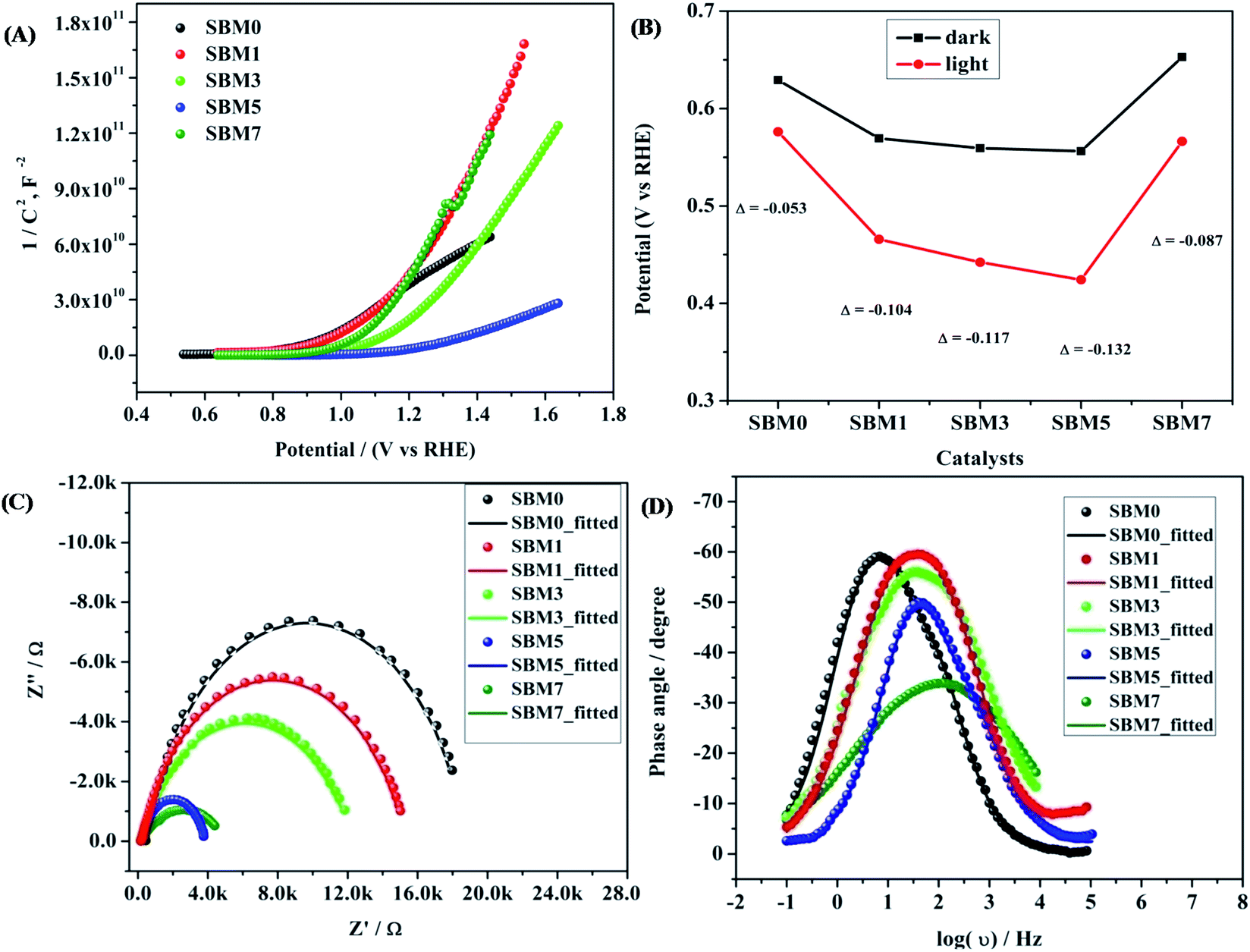
For further insight into the charge transfer and separation process, Mott–Schottky analysis was carried out; the scans were recorded in the potential window from 0.64 V to 1.64 V (vs. RHE) with an increment of 0.025 V at 100 Hz frequency as shown in Fig. 5A.
| |
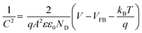 | (5) |
where
C (F) is space charge capacitance,
q is elementary charge,
A is electrode surface area,
ε is relative permittivity of BiVO
4 (68),
90 ε0 vacuum permittivity (8.854 × 10
−12 Fm
−1),
ND (cm
−3) is donor density,
V is applied potential,
VFB is flat band potential and
kB is Boltzmann constant (1.38 × 10
−23 J K
−1) and
T is absolute temperature. From the slope of a plot of 1/
C2 vs. V, donor density is measured, which is the inherent property of photoanode materials. Donor density was calculated from the slope of
Fig. 5A and tabulated in
Table 3.
ND of SBM0 is found as 5.23 × 10
19 cm
−3, the measured value is in accordance with the literature reports.
68,69,88 Upon doping of Mo, donor density is found to increase, and the values in samples SBM1, SBM3, SBM5, and SBM7 are obtained as 6.24 × 10
19, 9.66 × 10
19, 3.85 × 10
20 and 8.82 × 10
19 cm
−3 respectively. This increase of donor density supports the increase of photocurrent with doping of Mo observed in chopped light voltammetry measurements.
68,88
 |
| | Fig. 5 (A) Mott–Schottky analysis for calculation of donor density and flat band potential, (B) OCPV calculation by measuring the difference in potential in dark and illumination, (C) Nyquist plot and (D) Bode plots of the BiVO4 based photoanodes. | |
Table 3 PEC activity of the photoanodes were characterized by the following parameters
| Catalysts |
Band gap (eV) |
% increase in photocurrent |
Donor density (cm−3) |
Flat band potential, V |
OCPV |
% of charge transfer efficiency@1.64 V |
% of charge transport efficiency@1.64 V |
| SBM0 |
2.54 |
— |
5.23 × 10¹⁹ |
0.94 |
−0.053 |
46.62 |
63.73 |
| SBM1 |
2.52 |
12.30 |
6.42 × 10¹⁹ |
1.09 |
−0.014 |
47.24 |
78.31 |
| SBM3 |
2.54 |
29.23 |
9.66 × 10¹⁹ |
1.16 |
−0.117 |
53.90 |
79.60 |
| SBM5 |
2.50 |
153.84 |
3.85 × 10²⁰ |
1.20 |
−0.132 |
50.23 |
176.27 |
| SBM7 |
2.53 |
63.08 |
8.82 × 10¹⁹ |
1.05 |
−0.087 |
50.02 |
95.68 |
Further, the flat band potential, which is also an important property of photoanode materials and qualitative measurement of the degree of band bending at the electrode–electrolyte interface,63,64,91 was calculated from Mott–Schottky plot as shown in Fig. 5A. At higher band bending, the electron–hole recombination will be difficult at the interface, which will result in the improvements of PEC efficiency and stabilizes the photoanodes.63–65,91 The flat band potential of SBM0 is found as 0.94 V, on Mo doping, the flat band potential is observed as, 1.09 V, 1.16 V, 1.20 V and 1.05 V for the samples SBM1, SBM3, SBM5, and SBM7 respectively. This observation suggests that the band bending is improved upon Mo doping up to the Mo doping of 5%, which resulted in the suppression of electron–hole recombination on the interface. The suppression of charge recombination facilitates higher charge transfer property at the interface, and hence, overall PEC efficiency is improved. The increase in the flat band potential thus supports the observed enhancement of current in chopped light voltammetry and an increase in the IPCE values on Mo doping up to 5%.
Band bending and charge separation efficiency were further investigated by open-circuit photovoltage (OCPV, Vph) measurements under AM 1.5 illumination. The extent of band bending is a qualitative measure of in-built potential and charge recombination.65,66 The OCPV was calculated from the difference in open circuit potential in dark and illumination as shown in Fig. 5B and tabulated in Table 3 for different samples investigated. OCPV of SBM0, SBM1, SBM3, SBM5 and SBM7 are obtained as −0.053 V, −0.104 V, −0.117 V, −0.132 V and −0.087 V respectively. The shifting of OCPV towards more cathodic side suggests a strong alternation of bands at the electrode–electrolyte interface with Mo doping. This change of OCPV, sourced from the higher band bending under photo-illumination, improves the overall catalytic efficiency by suppressing of charge recombination and improvement of charge separation at the interface. The OCPV is basically the difference between the Fermi levels of the semiconductor when in dark and under illuminated conditions, which is improved on Mo doping. The Fermi level of the semiconductor under illumination, bends to lower its energy, due to which the open circuit voltage differs from that in the dark. The Fermi level bending and the enhancement of OCPV have been schematically shown in Fig. S3 of the ESI.†65 On Mo doping the Fermi level undergo enhanced bending, which enhances the OCPV up to the Mo content of 5%. The increase in the OCPV resulted in the improvement of photocurrent on doping of Mo in BiVO4.
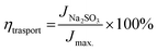
The interfacial charge transfer efficiency and charge transport efficiency are two limiting parameters on which the overall efficiency of PEC depends. Charge transfer and transport efficiency measurements were performed using a hole scavenger method.92,93 LSV was recorded in 0.1 M PBS for water splitting. Hole scavenger Na2SO3 (0.1 M solution) was used by assuming complete and fast oxidation of sulfite; the LSV plots are shown in Fig. S4 (ESI†). Then, current densities were sampled at 1.64 V and ηtranfer and ηtrasport were calculated using following equations.
| |
 | (6) |
| |
 | (7) |
| |
 | (8) |
where,
Jmax. was calculated from the photocurrent obtained from the silicon diode detector.
JH2O is the current density for water oxidation;
JNa2SO3 is the current density for the oxidation of sulfite. Since the water oxidation process is sluggish, sodium sulfite was used as a hole scavenger. It is supposed that oxidation of sulfite is 100%; thus the charge transfer efficiency was calculated with respect to 100% faradaic efficient,
i.e. how fast charge gets transferred from the electrode–electrolyte interface to water molecule for oxidation. The charge transfer efficiency was calculated and tabulated in
Table 3. For SBM0, the charge transfer efficiency is calculated as 46.62%. Doping of Mo in BiVO
4 resulted in the enhancement of charge transfer efficiency by 15% from the SBM0 sample. The improvement of charge transfer efficiency at the interface is attributed from higher band bending upon Mo doping and increases in donor density as obtained from Mott–Schottky analysis and OCPV measurements. Charge transport efficiency is another factor that greatly affects the photocatalytic activity, it was calculated based on the charge generated inside the photoanode material, and the fraction of it gets transferred at the interface. The charge transport efficiency for SBM0 is obtained as 63.73%. The charge transport efficiency of other samples SBM1, SBM3, SBM5, and SBM7 are 78.31%, 79.66%, 176.27%, and 95.27%, respectively (
cf. Table 3). These values suggest that band bending upon Mo doping improves charge transport and suppressed the recombination process, as suggested by Mott–Schottky analysis and OCPV values. Thus the improvements of charge transfer and transport efficiencies are the factors responsible for enhancement in the PEC efficiency and support chopped light voltammetry results and IPCE measurements.
Electrochemical impedance measurements
The conductivity and charge transfer resistance are measured from the analysis of Nyquist plot; it also provides the qualitative insight of the charge transfer processes in bulk as well as at the interface of the photoanode, corresponding results are shown in Fig. 5C. Impedance results are fitted with the equivalent circuit as shown in Fig. S5 (in ESI†) and the fitting parameters are tabulated in Table 4. Rct value of SBM0 is found as 16.8 kΩ. When Mo is doped, Rct values decreased considerably. The decrease in Rct value suggests faster charge transfer at the interface on Mo doping. This variation in Rct values supports the PEC activity measurements. The photoanodes were further characterized for their charge relaxation processes from Bode plot analysis as shown in Fig. 5D. Frequencies of phase maxima were sampled for different catalysts, which correspond to the relaxation frequency of photogenerated charge and the results are summarized in Table 4. The relaxation frequency of the SBM0 sample is 6.88 Hz, and the relaxation frequency is increased linearly with the Mo doping from SBM0 to SBM7. Further, the relaxation time constant (τ) of the electrochemical process was calculated using τ = 1/2πf where f is relaxation frequency. The decrease in τ indicates the faster electrochemical process on Mo doping, which supports the improvements in the PEC efficiency.
Table 4 Impedance spectroscopy analysis of photoanodes for measurements of bulk and surface characterization
| Catalysts |
Rct (Ω) |
Ctotal (F) |
Relaxation frequency (Hz) |
Relaxation time constant (ms) |
LD (μm) |
| SBM0 |
16820 |
8.33 × 10⁻⁶ |
6.88 |
23.12 |
340 |
| SBM1 |
15060 |
4.43 × 10⁻⁶ |
32.36 |
4.92 |
157 |
| SBM3 |
12010 |
4.24 × 10⁻⁶ |
32.36 |
4.92 |
157 |
| SBM5 |
3610 |
1.18 × 10⁻⁵ |
44.36 |
3.56 |
134 |
| SBM7 |
4832 |
1.16 × 10⁻⁵ |
91.20 |
1.75 |
94 |
Diffusion length is an important parameter in characterizing the interfacial processes, and the overall PEC efficiency depends heavily on the hole diffusion process. The measurement of the diffusion length from impedance measurements, however, includes the assumption that the relaxation time constant is the time taken by the hole to oxidize the water molecule, which contains the diffusion of the hole inside the films and also its diffusion at the electrolyte interface to oxide water molecule. Diffusion length of the photo-generated holes is calculated by using the equation, LD = (D × τ)2 where LD is diffusion length, D is the diffusion coefficient of the photogenerated hole, taken as 0.05 cm2 s−1,94 and τ is the relaxation time, the values as obtained are tabulated in Table 4. LD of SBM0 is found to be 340 μm. The diffusion length thus obtained from the impedance measurements is decreased with the Mo doping in BiVO4. The measured diffusion process includes the diffusion inside the solid catalysts and also at the interface since the observed diffusion length is significantly higher compared to the thickness of the films, the holes are expected to be transported outside the electrochemical interface. The thickness of the films has a negligible contribution to the overall measured diffusion length of the material. The lower diffusion length at the electrochemical interface is associated with the fast charge transfer process at the interface, which is expected to have a higher PEC current.
As seen from Table 4 the capacitance of the SBM0 is significantly low (8.33 × 10⁻⁶ F) compared to the materials containing Mo. The observed capacitance improvement on the addition of Mo indicates the significant improvement in the surface charge density on the incorporation of Mo in BiVO4. These results show that there are surface improvements as well with the improvements in the bulk property of the photoanode upon Mo doping in the BiVO4, which enhances the overall PEC efficiency.
Testing of stability of the photoanodes
Stability of photoanode materials is important for prolonged application of the catalyst; it was performed using chronoamperometry technique at 1.44 V vs. RHE with chopped light voltammetry method, as shown in Fig. 6, the photocurrent of SBM0 was decreased by 37% after initial excitation. On Mo doping, the recombination step has been reduced drastically, and in place of decay in current, growth in the photocurrent response is observed. The stability test was further performed for continuous illumination of light for 900 s, as shown in Fig. S6 (in (ESI†)) for two catalyst samples. In both, the samples SBM1 and SBM5, the photocurrent is improved initially and then stabilized. The improvement of photocurrent is observed previously and explained on the basis of the charging effect of the photoanode.95,96 The photocharging effect has been discussed based on both the surface and bulk modifications in the materials. The redox reaction through the transformation of V(V) to V(IV) is discussed as one of the important reasons behind the enhanced photocurrent due to photocharging. The photocharging effect is observed to be enhanced in the present case on the incorporation of Mo in the catalyst. The reduction potential of V(V) to V(IV) is more positive than the Mo(VI) to Mo(V) reduction; however, the redox kinetics in the later case is significantly faster.97 In view of this, during photocharging process, Mo(VI) will get reduced to Mo(V) first due to the kinetic effect; afterward Mo(V) would transfer the electron to V(V) and facilitate the reduction of V(V) to V(IV). As reported previously, this facilitated reduction of V(V) to V(IV) due to the presence of Mo would enhance the catalytic activity on photocharging.95 The photocharging effect is also discussed to be due to the interfacial factor through the modification of band structure upon photocharging. The OCPV is measured in all the materials; its value is increased with the Mo doping. The increase in the OCPV can be correlated with the relatively more significant bending of the conduction band than the valence band under photo-illumination. The increase in the OCPV indicates the lesser possibility of recombination and enhancement of the hole transfer property through the interface, which eventually would increase the PEC catalytic process in the material.65,66
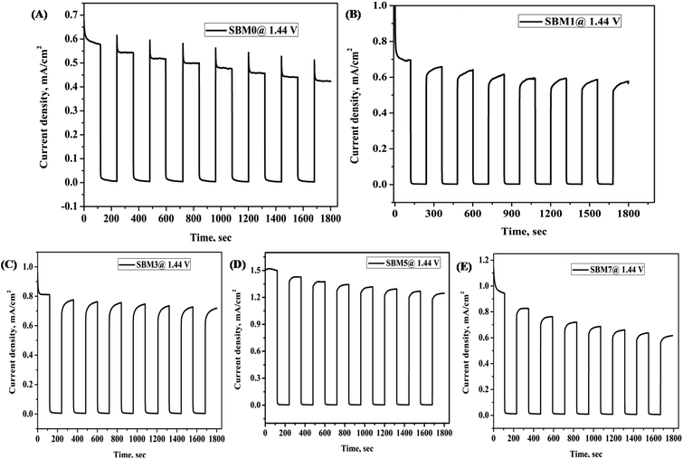 |
| | Fig. 6 All BiVO4 based photoanode was characterized for stability test by chopped light voltammetry at 0.8 V vs. Ag/AgCl for 1800 s (A) SBM0, (B) SBM1, (C) SBM3, (D) SBM5 and (E) SBM7. | |
Interfacial charge transfer kinetics using SECM
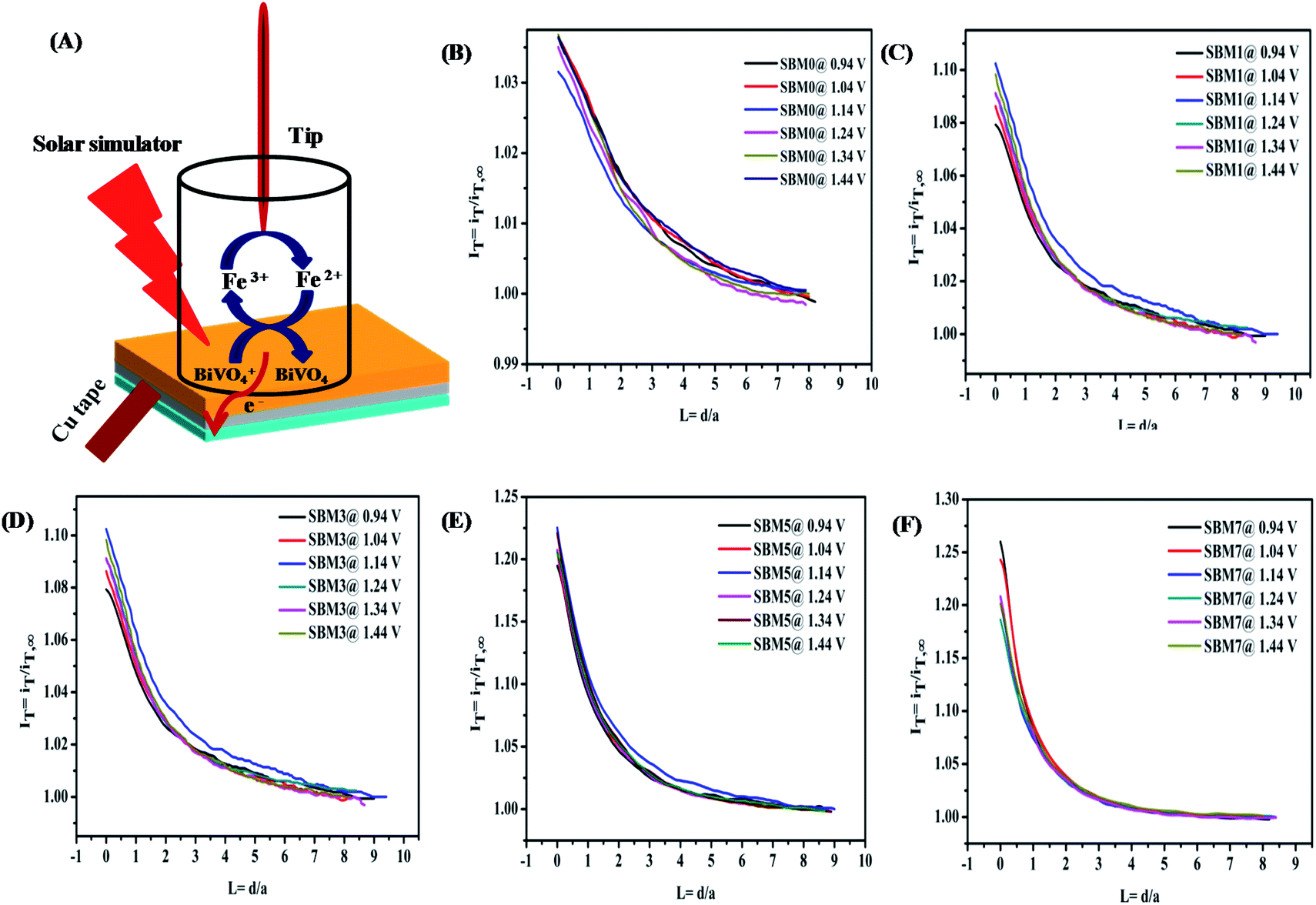
The charger transfer at the semiconductor–electrolyte interface and quantification of the active sites in in situ measurements have been performed by the SECM technique.98–103 Investigation of the interface has been carried out by the tip feedback mode. When a tip is far from any surface, tip current, iT,∞ depends on the number of electrons transferred, concentration of electroactive species, diffusion coefficient and radius of ultra-microelectrode.98 When the surface is an insulator, the tip current is iTiT,∞ which results negative feedback. When surface is conducting, redox active species is generated at the surface, tip current, iTiT,∞ as a result, positive feedback is observed.
In PEC water oxidation reaction, photogenerated holes at the BiVO4 interface oxidize water to form oxygen. Since the direct investigation of the water oxidation intermediate or oxygen at the BiVO4 surface in the feedback mode is technically difficult, the redox probe [Fe(CN)6]3−/[Fe(CN)6]4− is used rather than the water oxidation intermediate or molecular oxygen.104 It has been reported that redox mediator [Fe(CN)6]4− and [Fe(CN)6]3− can be used as the acceptor of the photogenerated holes and electrons to characterize the redox kinetics of the photo-catalyst for the PEC water-splitting reaction.105 Fig. 7A shows the schematics of the reaction at the BiVO4 interface in the feedback approach. The photogenerated hole at the photoanode/electrolyte interface oxidizes the [Fe(CN)6]4− to the [Fe(CN)6]3−. There is large driving force (ΔG ∼ −2.0 eV) for transfer of the photogenerated hole from the valence band of BiVO4 to [Fe(CN)6]4− for oxidation at the surface catalytic reaction. Therefore, the hole transfer from a valence band of BiVO4 to [Fe(CN)6]4− is kinetically more favorable by ΔG ∼ −0.4 eV than the water oxidation.106 The cathodic potential at the probe is tuned to the reduction potential of [Fe(CN)6]3− to [Fe(CN)6]4− so that there is no side reaction such as oxygen reduction take place. Therefore, feedback current can be assumed mainly from the reduction of [Fe(CN)6]3−. The hole transfer kinetics at BiVO4/interface is measured by the feedback current of the reduction of [Fe(CN)6]3− in dark and illumination conditions. In the dark, photoanode behaves as an insulator because of the non-availability of the free electron or hole at the interface and hence negative feedback is observed, however on illumination, it behaves as conducting substrate because of photogenerated holes and electrons. The photogenerated holes at the interface oxidize [Fe(CN)6]4− to [Fe(CN)6]3−, [Fe(CN)6]3− species diffuses to the probe and increases the mass transfer process, resulting in the positive feedback response. The normalized tip current (IT) is calculated by using IT = iT/iT,∞ where, iT is the real time tip current during the approach to the substrate electrode and iT,∞ is steady current of the tip when the tip is far from the substrate. Prior to the approach of the probe to the substrate, the CV of ultra microelectrode was performed in 2 mM ferricyanide solution as shown in Fig. S7A† shows a good response from the probe. The negative feedback response was fitted using eqn (S1)† for the measurement of RG value. The positive feedback response under illumination was used for the hole kinetics measurements. The positive feedback response of all photoanodes are shown in Fig. 7, the observation of positive feedback indicates the transfer of a hole from the illuminated electrode surface. The normalized apparent heterogeneous charge transfer rate constant (κ) and effective heterogeneous charge transfer rate constant κeff (in cm s−1) at BiVO4/electrolyte interface is obtained from the fitting of experiment approach curve to the theoretical SECM kinetics model using eqn (S1)–(S6).†107
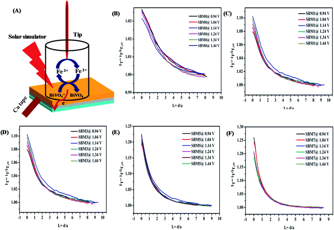 |
| | Fig. 7 (A) The proposed mechanism of feedback mode of analysis of BiVO4/electrolyte interface by SECM analysis. In this technique, a 2 mM ferricyanide solution was used as the redox mediator. In illumination, photo-generated holes oxidizes the [Fe(CN)6]4− to [Fe(CN)6]3− at the interface and the cathodic potential applied at probe reduces the photo-oxidized [Fe(CN)6]3− to [Fe(CN)6]4−. This redox close-loop gives positive feedback in illumination and negative feedback in dark conditions. SECM imaging of the surface is characterized by the measuring of probe current to measure the hole transfer from the interface to the [Fe(CN)6]4−. Normalized SECM feedback approach curve of the BiVO4 based photoanodes (B) SBM0, (C) SBM1, (D) SBM3, (E) SBM5 and (F) SBM7 in 2 mM [Fe(CN)6]3− solution at different applied bias potential at substrate under illumination using Pt ultra microelectrode having rT value 4.5 μm as calculated from the cyclic voltammetry measurement shown in (ESI) Fig. S6A.† | |
All approach curves have been numerically fitted using the above equation and then kinetics parameters are calculated. Some of the fittings of the approach plots are shown in Fig. S8 of the (ESI).† The effective heterogeneous charge transfer rate constant keff is calculated using the relation keff = κDdiffusion/rT where Ddiffusion is the diffusion coefficient of the redox probe [Fe(CN)6]3− and tabulated in Table 5. The low value of keff for SBM0 shows sluggish hole transfer process at the interface. When Mo was doped in to the BiVO4 hole transfer rate constant is found to improve significantly. This improvement suggests that interfacial charge transfer is facilitated upon Mo doping. Further, the effect of applied bias on the hole transfer rate constant is investigated by approaching the probe at different applied potentials. The rate constant for all the materials remained unchanged with the applied potentials indicating its limiting value even at lowest applied potential.
Table 5 The keff of hole transfer from the BiVO4/electrolyte interface to [Fe(CN)6]3−
| keff (in 10−3 cm s−1) |
| Potential, V |
SBM0 |
SBM1 |
SBM3 |
SBM5 |
SBM7 |
| 0.94 |
2.18 |
3.58 |
4.25 |
6.80 |
7.50 |
| 1.04 |
2.18 |
3.90 |
4.12 |
7.16 |
7.48 |
| 1.14 |
2.18 |
4.25 |
4.40 |
7.56 |
7.16 |
| 1.24 |
2.18 |
4.0 |
4.25 |
7.16 |
6.48 |
| 1.34 |
2.18 |
4.0 |
4.25 |
7.56 |
7.16 |
| 1.44 |
2.18 |
4.25 |
4.25 |
7.16 |
7.16 |
The localized PEC activity of the BiVO4 photoanodes was analyzed by imaging the surface in the constant height mode at the applied potentials of 0.94 V and 1.14 V to the substrate. A cathodic potential of 0.64 V was applied to the probe for the reduction of the [Fe(CN)6]3− to [Fe(CN)6]4−. Therefore, during imaging of the substrate, feedback current at the probe was monitored, and the images are shown in Fig. S9 to S11.† The catalyst substrate is mapped with various current regions, and the current response is increased marginally with more anodic applied potential to the substrate. The overall current response of the tip scanned over the substrate is increased with Mo doping in BiVO4 up to 5% doping level. The images are further characterized with bigger current region at doping level up to 5%, originated from the overlapping diffusion layer across the catalyst substrate. At 7% doping, in place of overlapping region, the catalytic currents are characterized by small patches separated from each other. The observation can be correlated from the separated grains at 7% doping compared to the overlapped diffusion layer structure in all other samples. Catalytic current obtained from the overlapping diffusion layer is beneficial in catalyst design, as it provides a similar catalytic activity to that of the continuous films requiring fewer amounts of catalysts. The SECM imaging thus further indicates the betterment in the catalytic activity on Mo doping and also reveals the regional distribution of the catalytic current over the catalyst substrates.
Results thus indicate significant improvement in the catalytic activity of BiVO4 through the inclusion of SnO2 heterojunction and doping of Mo, which has been explained using some of the important interfacial measurements.
Conclusion
Present investigation was aimed to improve the photoelectrocatalytic efficiency of BiVO4 through the incorporation of SnO2 interlayer and doping of Mo. The significant improvement (∼154%) in the photocurrent was observed upon 5% Mo doping in SnO2/BiVO4. Strong correlation among the optical property of the material, the open circuit photovoltage (OCPV), and onset potential was observed in relation to the improvement in the PEC efficiency on Mo doping. The increase in the flat band potential and OCPV suggests the improvements in the charge separation upon the Mo doping which resulted in the enhancement in PEC efficiency. SECM investigation reveals significant improvement in effective hole transfer rate constant from 2.18 cm s−1 to 7.56 cm s−1 with the Mo doping in BiVO4. The electrochemical impedance investigation supports the improvements in the charge transfer and transport efficiency by improvements in the bulk and surface properties of BiVO4. The facilitated reduction of V(V) to V(IV) on Mo doping is also responsible for the improvement in the catalytic activity. The improvement in the catalytic activity has been evaluated from the improvement in the physicochemical at the bulk of the catalysts, its surface, and most importantly due to the improvement in its interfacial charge transfer processes. Mild expansion in the crystal lattice is also observed on replacement of V by Mo, the improvement in the catalytic activity however, related primarily to the electronic nature compared to any morphological changes.
Abbreviations
| SEM | Scanning electron microscope |
| EDS | Energy dispersive spectroscopy |
| XPS | X-ray photoelectron spectroscopy |
| CV | Cyclic voltammetry |
| LSV | Linear sweep voltammetry |
| PEC | Photo-electrocatalysis |
| EIS | Electrochemical impedance spectroscopy |
| OCPV | Open-circuit photovoltage |
| UME | Ultra-microelectrode |
| PAC | Probe approach curve |
| SECM | Scanning electrochemical microscopy |
Author contributions
The manuscript was written through the contributions of all authors. All authors have given approval to the final version of the manuscript.
Funding sources
This project is fully funded by our institute Bhabha Atomic Research Centre, Government of India.
Conflicts of interest
All the authors of this manuscript declare that there is no conflicts of interest exists to disclose.
Acknowledgements
We thank Dr H. Pal, Associate Director, Chemistry Group (A), Bhabha Atomic Research Centre for his encouragement and support during the course of the present work.
References
- J. Turner, Int. J. Energy Res., 2008, 32, 379–407 CrossRef CAS.
- C. Du, J. Mo and H. Li, Chem. Rev., 2014, 115, 1503–1542 CrossRef PubMed.
- M. G. Walter, E. L. Warren, J. R. McKone, S. W. Boettcher, Q. Mi, E. A. Santori and N. S. Lewis, Chem. Rev., 2010, 110, 6446–6473 CrossRef CAS PubMed.
- T. Faunce, S. Styring, M. R. Wasielewski, G. W. Brudvig, A. W. Rutherford, J. Messinger, A. F. Lee, C. L. Hill, H. Degroot and M. Fontecave, Energy Environ. Sci., 2013, 6, 1074–1076 RSC.
- T. Hisatomi, J. Kubota and K. Domen, Chem. Soc. Rev., 2014, 43, 7520–7535 RSC.
- M. D. Bhatt and J. S. Lee, J. Mater. Chem. A, 2015, 3, 10632–10659 RSC.
- S. Wang, H. Chen, G. Gao, T. Butburee, M. Lyu, S. Thaweesak, J.-H. Yun, A. Du, G. Liu and L. Wang, Nano Energy, 2016, 24, 94–102 CrossRef CAS.
- P. Peerakiatkhajohn, J. H. Yun, H. Chen, M. Lyu, T. Butburee and L. Wang, Adv. Mater., 2016, 28, 6405–6410 CrossRef CAS PubMed.
- C. Zhen, R. Chen, L. Wang, G. Liu and H.-M. Cheng, J. Mater. Chem. A, 2016, 4, 2783–2800 RSC.
- S. Kment, F. Riboni, S. Pausova, L. Wang, L. Wang, H. Han, Z. Hubicka, J. Krysa, P. Schmuki and R. Zboril, Chem. Soc. Rev., 2017, 46, 3716–3769 RSC.
- S. Wang, P. Chen, J. H. Yun, Y. Hu and L. Wang, Angew. Chem., Int. Ed., 2017, 56, 8500–8504 CrossRef CAS PubMed.
- T. Butburee, Y. Bai, H. Wang, H. Chen, Z. Wang, G. Liu, J. Zou, P. Khemthong, G. Q. M. Lu and L. Wang, Adv. Mater., 2018, 30, 1705666 CrossRef PubMed.
- S.-C. Wang, F.-Q. Tang and L.-Z. Wang, J. Inorg. Mater., 2018, 33, 173–196 CrossRef.
- S. n. Murcia-López, C. Fàbrega, D. n. Monllor-Satoca, M. a. D. Hernández-Alonso, G. n. Penelas-Pérez, A. Morata, J. R. Morante and T. Andreu, ACS Appl. Mater. Interfaces, 2016, 8, 4076–4085 CrossRef PubMed.
- T. W. Kim and K.-S. Choi, Science, 2014, 343, 990–994 CrossRef CAS PubMed.
- E. A. Mohamed, Z. N. Zahran and Y. Naruta, J. Mater. Chem. A, 2017, 5, 6825–6831 RSC.
- L. Zhou, C. Zhao, B. Giri, P. Allen, X. Xu, H. Joshi, Y. Fan, L. V. Titova and P. M. Rao, Nano Lett., 2016, 16, 3463–3474 CrossRef CAS PubMed.
- F. F. Abdi, N. Firet and R. van de Krol, ChemCatChem, 2013, 5, 490–496 CrossRef CAS.
- C. Zachäus, F. F. Abdi, L. M. Peter and R. Van De Krol, Chem. Sci., 2017, 8, 3712–3719 RSC.
- B. J. Trześniewski, I. A. Digdaya, T. Nagaki, S. Ravishankar, I. Herraiz-Cardona, D. A. Vermaas, A. Longo, S. Gimenez and W. A. Smith, Energy Environ. Sci., 2017, 10, 1517–1529 RSC.
- Y. Ma, S. R. Pendlebury, A. Reynal, F. Le Formal and J. R. Durrant, Chem. Sci., 2014, 5, 2964–2973 RSC.
- H. W. Jeong, T. H. Jeon, J. S. Jang, W. Choi and H. Park, J. Phys. Chem. C, 2013, 117, 9104–9112 CrossRef CAS.
- K. J. McDonald and K.-S. Choi, Energy Environ. Sci., 2012, 5, 8553–8557 RSC.
- V. Nair, C. L. Perkins, Q. Lin and M. Law, Energy Environ. Sci., 2016, 9, 1412–1429 RSC.
- Z.-F. Huang, L. Pan, J.-J. Zou, X. Zhang and L. Wang, Nanoscale, 2014, 6, 14044–14063 RSC.
- H. L. Tan, R. Amal and Y. H. Ng, ACS Appl. Mater. Interfaces, 2016, 8, 28607–28614 CrossRef CAS PubMed.
- J. Su, L. Guo, N. Bao and C. A. Grimes, Nano Lett., 2011, 11, 1928–1933 CrossRef CAS PubMed.
- Y. Pihosh, I. Turkevych, K. Mawatari, J. Uemura, Y. Kazoe, S. Kosar, K. Makita, T. Sugaya, T. Matsui and D. Fujita, Sci. Rep., 2015, 5, 11141 CrossRef PubMed.
- J.-S. Yang and J.-J. Wu, Nano Energy, 2017, 32, 232–240 CrossRef CAS.
- L. H. Hess, J. K. Cooper, A. Loiudice, C.-M. Jiang, R. Buonsanti and I. D. Sharp, Nano Energy, 2017, 34, 375–384 CrossRef CAS.
- P. M. Rao, L. Cai, C. Liu, I. S. Cho, C. H. Lee, J. M. Weisse, P. Yang and X. Zheng, Nano Lett., 2014, 14, 1099–1105 CrossRef CAS PubMed.
- Z. Zhang, B. Chen, M. Baek and K. Yong, ACS Appl. Mater. Interfaces, 2018, 10, 6218–6227 CrossRef CAS PubMed.
- L. Zhou, Y. Yang, J. Zhang and P. M. Rao, ACS Appl. Mater. Interfaces, 2017, 9, 11356–11362 CrossRef CAS PubMed.
- H. Jung, S. Y. Chae, C. Shin, B. K. Min, O.-S. Joo and Y. J. Hwang, ACS Appl. Mater. Interfaces, 2015, 7, 5788–5796 CrossRef CAS PubMed.
- S. P. Berglund, A. J. Rettie, S. Hoang and C. B. Mullins, Phys. Chem. Chem. Phys., 2012, 14, 7065–7075 RSC.
- F. F. Abdi, L. Han, A. H. Smets, M. Zeman, B. Dam and R. Van De Krol, Nat. Commun., 2013, 4, 2195 CrossRef PubMed.
- W. Luo, Z. Yang, Z. Li, J. Zhang, J. Liu, Z. Zhao, Z. Wang, S. Yan, T. Yu and Z. Zou, Energy Environ. Sci., 2011, 4, 4046–4051 RSC.
- S. K. Pilli, T. E. Furtak, L. D. Brown, T. G. Deutsch, J. A. Turner and A. M. Herring, Energy Environ. Sci., 2011, 4, 5028–5034 RSC.
- M. Rohloff, B. Anke, O. Kasian, S. Zhang, M. Lerch, C. Scheu and A. Fischer, ACS Appl. Mater. Interfaces, 2019, 11, 16430–16442 CrossRef CAS PubMed.
- S. Byun, G. Jung, S.-Y. Moon, B. Kim, J. Y. Park, S. Jeon, S.-W. Nam and B. Shin, Nano energy, 2018, 43, 244–252 CrossRef CAS.
- M. Huang, J. Bian, W. Xiong, C. Huang and R. Zhang, J. Mater. Chem. A, 2018, 6, 3602–3609 RSC.
- G. Wang, Y. Yang, Y. Ling, H. Wang, X. Lu, Y.-C. Pu, J. Z. Zhang, Y. Tong and Y. Li, J. Mater. Chem. A, 2016, 4, 2849–2855 RSC.
- J.-M. Wu, Y. Chen, L. Pan, P. Wang, Y. Cui, D. Kong, L. Wang, X. Zhang and J.-J. Zou, Appl. Catal., B, 2018, 221, 187–195 CrossRef CAS.
- Y. Bu, J. Tian, Z. Chen, Q. Zhang, W. Li, F. Tian and J. P. Ao, Adv. Mater. Interfaces, 2017, 4, 1601235 CrossRef.
- M. R. Nellist, J. Qiu, F. A. Laskowski, F. M. Toma and S. W. Boettcher, ACS Energy Lett., 2018, 3, 2286–2291 CrossRef CAS.
- M. Zhong, T. Hisatomi, Y. Kuang, J. Zhao, M. Liu, A. Iwase, Q. Jia, H. Nishiyama, T. Minegishi and M. Nakabayashi, J. Am. Chem. Soc., 2015, 137, 5053–5060 CrossRef CAS PubMed.
- M. Liao, J. Feng, W. Luo, Z. Wang, J. Zhang, Z. Li, T. Yu and Z. Zou, Adv. Funct. Mater., 2012, 22, 3066–3074 CrossRef CAS.
- F. F. Abdi and R. van de Krol, J. Phys. Chem. C, 2012, 116, 9398–9404 CrossRef CAS.
- D. K. Zhong, M. Cornuz, K. Sivula, M. Grätzel and D. R. Gamelin, Energy Environ. Sci., 2011, 4, 1759–1764 RSC.
- F. S. Hegner, I. Herraiz-Cardona, D. Cardenas-Morcoso, N. r. López, J.-R. n. Galán-Mascarós and S. Gimenez, ACS Appl. Mater. Interfaces, 2017, 9, 37671–37681 CrossRef CAS PubMed.
- M. Rohloff, B. Anke, S. Zhang, U. Gernert, C. Scheu, M. Lerch and A. Fischer, Sustainable Energy Fuels, 2017, 1, 1830–1846 RSC.
- X. Cao, C. Xu, X. Liang, J. Ma, M. Yue and Y. Ding, Appl. Catal., B, 2020, 260, 118136 CrossRef CAS.
- T. Tian, C. Dong, X. Liang, M. Yue and Y. Ding, J. Catal., 2019, 377, 684–691 CrossRef CAS.
- B. Klahr, S. Gimenez, F. Fabregat-Santiago, J. Bisquert and T. W. Hamann, J. Am. Chem. Soc., 2012, 134, 16693–16700 CrossRef CAS PubMed.
- J. Kwak and A. J. Bard, Anal. Chem., 1989, 61, 1221–1227 CrossRef CAS.
- C. M. Sánchez-Sánchez, J. Rodríguez-López and A. J. Bard, Anal. Chem., 2008, 80, 3254–3260 CrossRef PubMed.
- F. Li and P. R. Unwin, J. Phys. Chem. C, 2015, 119, 4031–4043 CrossRef CAS.
- P. Bertoncello, Energy Environ. Sci., 2010, 3, 1620–1633 RSC.
- B. C. Shah and A. C. Hillier, J. Electrochem. Soc., 2000, 147, 3043–3048 CrossRef CAS.
- H. Ye, J. Lee, J. S. Jang and A. J. Bard, J. Phys. Chem. C, 2010, 114, 13322–13328 CrossRef CAS.
- D. Zigah, J. Rodríguez-López and A. J. Bard, Phys. Chem. Chem. Phys., 2012, 14, 12764–12772 RSC.
- H. S. Park, K. C. Leonard and A. J. Bard, J. Phys. Chem. C, 2013, 117, 12093–12102 CrossRef CAS.
- K. Gelderman, L. Lee and S. Donne, J. Chem. Educ., 2007, 84, 685 CrossRef CAS.
- W. J. Albery, G. J. O'Shea and A. L. Smith, J. Chem. Soc., Faraday Trans., 1996, 92, 4083–4085 RSC.
- J. E. Thorne, S. Li, C. Du, G. Qin and D. Wang, J. Phys. Chem. Lett., 2015, 6, 4083–4088 CrossRef CAS PubMed.
- B. Iandolo, B. Wickman, I. Zorić and A. Hellman, J. Mater. Chem. A, 2015, 3, 16896–16912 RSC.
- J. H. Baek, B. J. Kim, G. S. Han, S. W. Hwang, D. R. Kim, I. S. Cho and H. S. Jung, ACS Appl. Mater. Interfaces, 2017, 9, 1479–1487 CrossRef CAS PubMed.
- K. Ding, B. Chen, Z. Fang, Y. Zhang and Z. Chen, Phys. Chem. Chem. Phys., 2014, 16, 13465–13476 RSC.
- Z. Zhao, W. Luo, Z. Li and Z. Zou, Phys. Lett. A, 2010, 374, 4919–4927 CrossRef CAS.
- D. Zhou, L.-X. Pang, W.-G. Qu, C. A. Randall, J. Guo, Z.-M. Qi, T. Shao and X. Yao, RSC Adv., 2013, 3, 5009–5014 RSC.
- S. Thalluri, C. Martinez-Suarez, A. Virga, N. Russo and G. Saracco, Int. J. Chem. Eng. Appl., 2013, 4, 305 CAS.
- D. Zhou, W. Qu, C. Randall, L. Pang, H. Wang, X. Wu, J. Guo, G. Zhang, L. Shui and Q. Wang, Acta Mater., 2011, 59, 1502–1509 CrossRef CAS.
- J. Yu and A. Kudo, Adv. Funct. Mater., 2006, 16, 2163–2169 CrossRef CAS.
- R. L. Frost, D. A. Henry, M. L. Weier and W. Martens, J. Raman Spectrosc., 2006, 37, 722–732 CrossRef CAS.
- F. D. Hardcastle and I. E. Wachs, J. Phys. Chem., 1991, 95, 5031–5041 CrossRef CAS.
- L. Chen, E. Alarcón-Lladó, M. Hettick, I. D. Sharp, Y. Lin, A. Javey and J. W. Ager, J. Phys. Chem. C, 2013, 117, 21635–21642 CrossRef CAS.
- J. Su, X.-X. Zou, G.-D. Li, X. Wei, C. Yan, Y.-N. Wang, J. Zhao, L.-J. Zhou and J.-S. Chen, J. Phys. Chem. C, 2011, 115, 8064–8071 CrossRef CAS.
- N. Myung, S. Ham, S. Choi, Y. Chae, W.-G. Kim, Y. J. Jeon, K.-J. Paeng, W. Chanmanee, N. R. de Tacconi and K. Rajeshwar, J. Phys. Chem. C, 2011, 115, 7793–7800 CrossRef CAS.
- C. D. Wagner, NIST Standarad Reference Database 20, 2000 Search PubMed.
- J.-G. Choi and L. Thompson, Appl. Surf. Sci., 1996, 93, 143–149 CrossRef CAS.
- K. P. S. Parmar, H. J. Kang, A. Bist, P. Dua, J. S. Jang and J. S. Lee, ChemSusChem, 2012, 5, 1926–1934 CrossRef CAS PubMed.
- X. Wan, F. Niu, J. Su and L. Guo, Phys. Chem. Chem. Phys., 2016, 18, 31803–31810 RSC.
- J. H. Kim, Y. H. Jo, J. H. Kim and J. S. Lee, Nanoscale, 2016, 8, 17623–17631 RSC.
- L. Zhang, Z. Dai, G. Zheng, Z. Yao and J. Mu, RSC Adv., 2018, 8, 10654–10664 RSC.
- L. Shi, S. Zhuo, M. Abulikemu, G. Mettela, T. Palaniselvam, S. Rasul, B. Tang, B. Yan, N. B. Saleh and P. Wang, RSC Adv., 2018, 8, 29179–29188 RSC.
- H. Luo, A. H. Mueller, T. M. McCleskey, A. K. Burrell, E. Bauer and Q. Jia, J. Phys. Chem. C, 2008, 112, 6099–6102 CrossRef CAS.
- J. Tauc, R. Grigorovici and A. Vancu, Phys. Status Solidi B, 1966, 15, 627–637 CrossRef CAS.
- W. Yao, H. Iwai and J. Ye, Dalton Trans., 2008, 1426–1430 RSC.
- Z. Chen, T. F. Jaramillo, T. G. Deutsch, A. Kleiman-Shwarsctein, A. J. Forman, N. Gaillard, R. Garland, K. Takanabe, C. Heske and M. Sunkara, J. Mater. Res., 2010, 25, 3–16 CrossRef CAS.
- M. Valant and D. Suvorov, J. Am. Ceram. Soc., 2000, 83, 2721–2729 CrossRef CAS.
- M. Etman, Electrochim. Acta, 1990, 35, 1195–1199 CrossRef CAS.
- I. S. Cho, C. H. Lee, Y. Feng, M. Logar, P. M. Rao, L. Cai, D. R. Kim, R. Sinclair and X. Zheng, Nat. Commun., 2013, 4, 1723 CrossRef PubMed.
- H. Dotan, K. Sivula, M. Grätzel, A. Rothschild and S. C. Warren, Energy Environ. Sci., 2011, 4, 958–964 RSC.
- H. S. Park, H.-W. Ha, R. S. Ruoff and A. J. Bard, J. Electroanal. Chem., 2014, 716, 8–15 CrossRef CAS.
- B. J. Trześniewski and W. A. Smith, J. Mater. Chem. A, 2016, 4, 2919–2926 RSC.
- E. Y. Liu, J. E. Thorne, Y. He and D. Wang, ACS Appl. Mater. Interfaces, 2017, 9, 22083–22087 CrossRef CAS PubMed.
- R. Cammack, M. J. Barber and R. C. Bray, Biochem. J., 1976, 157, 469–478 CrossRef CAS PubMed.
- A. J. Bard and M. V. Mirkin, Scanning electrochemical microscopy, CRC Press, 2012 Search PubMed.
- J. M. Barforoush, T. E. Seuferling, D. T. Jantz, K. R. Song and K. C. Leonard, ACS Appl. Energy Mater., 2018, 1, 1415–1423 CrossRef CAS.
- J. Y. Kim, H. S. Ahn and A. J. Bard, Anal. Chem., 2018, 90, 3045–3049 CrossRef CAS PubMed.
- T. Sun, D. Wang, M. V. Mirkin, H. Cheng, J.-C. Zheng, R. M. Richards, F. Lin and H. L. Xin, Proc. Natl. Acad. Sci. U. S. A., 2019, 116, 11618–11623 CAS.
- P. Li, Z. Jin, Y. Qian, Z. Fang, D. Xiao and G. Yu, ACS Energy Lett., 2019, 4, 1793–1802 CrossRef CAS.
- J. M. Barforoush, D. T. Jantz, T. E. Seuferling, K. R. Song, L. C. Cummings and K. C. Leonard, J. Mater. Chem. A, 2017, 5, 11661–11670 RSC.
- N. L. Ritzert, J. n. Rodríguez-López, C. Tan and H. c. D. Abruña, Langmuir, 2013, 29, 1683–1694 CrossRef CAS PubMed.
- J. Wang, J. Zhao and F. Osterloh, Energy Environ. Sci., 2015, 8, 2970–2976 RSC.
- B. Zhang, X. Zhang, X. Xiao and Y. Shen, ACS Appl. Mater. Interfaces, 2016, 8, 1606–1614 CrossRef CAS PubMed.
- R. Cornut and C. Lefrou, J. Electroanal. Chem., 2008, 621, 178–184 CrossRef CAS.
Footnote |
| † Electronic supplementary information (ESI) available. See DOI: 10.1039/c9ra08743e |
|
| This journal is © The Royal Society of Chemistry 2019 |
Click here to see how this site uses Cookies. View our privacy policy here. 
 Open Access Article
 This Open Access Article is licensed under a
  *ab
*ab