
 Open Access Article
 This Open Access Article is licensed under a Creative Commons Attribution-Non Commercial 3.0 Unported Licence
Biaxial strain modulated the electronic structure of hydrogenated 2D tetragonal silicene
Haoran Tuc,
Jing Zhanga,
Zexuan Guoa and
Chunyan Xu *ab
*ab
aInstitute for Interdisciplinary Quantum Information Technology, Jilin Engineering Normal University, Changchun 130052, China. E-mail: xcy@jlenu.edu.cn
bJilin Engineering Laboratory for Quantum Information Technology, Changchun 130052, China
cKey Laboratory of Physics and Technology for Advanced Batteries (Ministry of Education), Department of Physics, Jilin University, Changchun 130012, China
First published on 19th December 2019
Abstract
Silicene-based materials have attracted great attention due to their easier incorporation into silicon-based devices and components. In addition to the reported hydrogenated 2D tetragonal silicene (γ-SiH), we propose two stable atomic configurations of hydrogenated 2D tetragonal silicene (α-SiH and β-SiH) based on first-principles calculation. The calculated results indicate hydrogenation can effectively open the band gap of 2D tetragonal silicene, α-SiH is a semiconductor with a direct band gap of 2.436 eV whereas β-SiH is indirect band gap of 2.286 eV. We also find that the electronic band structure of α-SiH, β-SiH and γ-SiH can be modulated via biaxial strain. By applying biaxial strain in the range of −10% to 12%, the band gap of α-SiH, β-SiH and γ-SiH can be tuned in a range of 1.732–2.585 eV. Furthermore, direct–indirect or indirect–direct transition can be induced under biaxial strain, showing a high degree of flexibility in electronic band structure. The research not only broadens the diversity of hydrogenated 2D tetragonal silicenes, but also provides more possibilities of their applications in spintronic devices.
1. Introduction
Silicene, as the cousin of graphene, has attracted great attention because of its easier incorporation into silicon-based devices and components. Silicene with a honeycomb structure is predicted to be stable and is studied theoretically.1–4 Experimentally, silicene has been synthesized on different substrates.5–8 Several two-dimensional (2D) allotropes of silicene have been proposed, such as MoS2-type silicene,9 tetra-silicene,10 trigonal dumbbell silicene, honeycomb dumbbell silicene, large honeycomb dumbbell silicene,11–13 and tetragonal silicone.14,15 The physical properties in these materials mainly stem from the symmetry of the crystal structure. So, it is highly desirable to study 2D allotropes of materials with different symmetries. A 2D tetragonal allotrope in a square lattice consisting of tetrarings is also predicted to exist, including group IV14–18 and V elements,19,20 2D BP21 and SiC,22 as well as transition-metal dichalcogenides.23,24 The above studies reveal that some of the reported 2D tetragonal allotropes are nodal line semimetals or topological insulators. Subsequently, hydrogenated tetragonal Ge was reported to have two stable configurations, these configurations have a wide band gap which can be further tuned by external strain.25 The recent study has found that 2D tetragonal silicene is stable and exhibits a nodal line semimetal nature.14 Additionally, hydrogenation could induce a semimetal–semiconductor transition in 2D tetragonal silicene, this hydrogenated configuration (γ-SiH) is stable. Depending on the ordered distributions of H atoms, some possible configurations for hydrogenated 2D tetragonal silicene can be proposed, and the details of their structural and electronic properties have not been illustrated yet.Hydrogenation can significantly change the properties of 2D materials and is reported to have potential applications in spintronic devices.26–29 Theoretical predictions have revealed hydrogenation is an effective method to tailor the electronic properties of 2D silicene-related materials, and some of them have been observed in the experiments.30–39 Recent studies have reported fully hydrogenated silicene becomes wide band gap semiconductor and the type of gap depending on its atomic conformation,31 whereas half hydrogenated silicene transforms to ferromagnetic semiconductor.32 In the experiments, half- and fully-hydrogenated silicene sheet have been studied and synthesized on Ag (1 1 1) substrate by using the scanning tunneling microscopy (STM), high-resolution electron energy loss spectroscopy (HREELS), angle-resolved photoelectron spectroscopy (ARPES) and low-energy electron diffraction (LEED).35–39 The above works indicate atomic adsorption on nanosheet can be controlled with atomic precision in the experiments, which encourages use to modulate the properties of Si-based materials via adsorption. Moreover, the recently have reported the hydrogenated zigzag and armchair dumbbell silicene are semiconductors with larger band gaps, and their band gap and features are sensitive to strains.30 To broaden the practical application of 2D silicon-based materials for spintronic devices, the band gap modulating is crucial. It is well known that strain engineering is a common way to tune the band gap of 2D materials. Experimentally, methods for introducing strain into 2D materials generally include bending technique, piezoelectric stretching, exploiting the thermal expansion mismatch, elongating the substrate and controlled wrinkling, and so on.40–46 For example, a direct–indirect transition is experimentally induced in monolayer WS2 by applying uniaxial strain.42 Monolayer 1T-HfS2 is predicted theoretically to undergo a semiconductor–metal transition when compressive strain is applied.47 The band gap of GaN monolayer can be modulated in the broad range of 4.44–2.27 eV by applying tensile strain.48 In addition, monolayer GeP has been predicted to induce the transition from an indirect band-gap semiconductor to a direct band-gap semiconductor by the applied compressive strain along a direction.49 It has been reported that external tensile strain can alter the band gap value of Ag6S2, and a direct–indirect transition occurs in Ag6S2 when the tensile strain exceeds a critical value.50
The above studies have revealed the properties of 2D materials can be tuned by surface modification and strain engineering. In this work, based on first-principles calculations, two stable atomic configurations of hydrogenated 2D tetragonal silicene (α-SiH and β-SiH) are proposed, and the stability, structural and electronic properties of them are illustrated. The effect of biaxial strain engineering on the structural and electronic properties of 2D hydrogenated tetragonal silicene (α-, β- and the reported γ-SiH) is also studied.
2. Computational details
All the calculations were based on the density functional theory (DFT) as implemented in the Vienna Ab initio Simulation Package (VASP).51–53 The electron–ion interactions were described by projector-augmented wave (PAW) method,54 and exchange–correlation functional was considered in the generalized gradient approximation (GGA)55 with Perdew–Burke–Ernzerhof (PBE) functional. The plane wave basis was set to be 500 eV and the Brillouin zone (BZ) was sampled of a 13 × 13 × 1 k-point mesh. All structures were fully relaxed until the force exerted on each atom was less than 0.01 eV Å−1 and the total energy change was smaller than 1 × 10⁻⁶ eV. A vacuum layer more than 20 Å was placed to minimize the interaction between periodic images along the z-direction. In addition, the hybrid Heyd–Scuseria–Ernzerhof (HSE06) functional56 was used to check the validity of the band gap given by the PBE method. The ab initio molecular dynamics (AIMD) simulations were implemented based on the NVT ensemble with a time step of 1 fs and the total simulation time of 10 ps. The phonon dispersions were performed by using the PHONOPY code.573. Results and discussion
Fig. 1 presents the optimized atomic configurations of hydrogenated 2D tetragonal silicene denoted by α-SiH, β-SiH and γ-SiH, respectively. The γ-SiH has been studied previously14 while α-SiH and β-SiH have not been investigated yet. In the case of α-SiH and β-SiH, the hydrogen atoms alternate in pairs of the sheet in different ways. For γ-SiH, the hydrogen atoms alternate on both sides of the sheet. All studied structures have a square lattice, each Si atom bonded with other three Si atoms and one H atom. The optimized structural parameters of these three configurations are summarized in Table 1. All the Si–Si bond lengths in three hydrogenated systems are larger than those in the pure tetragonal silicene. The buckled height h0 of α-SiH is much larger than those of β-SiH and γ-SiH, and they are larger than the buckled height h0 of pure tetragonal silicene. The hydrogenated 2D tetragonal silicene (γ-SiH) is stable that has been reported previously.14 So next we just discuss the stability of α-SiH and β-SiH by calculating the binding energy, phonon dispersions and AIMD simulations. The binding energy for hydrogenated 2D tetragonal silicene defined by Eb = (ESiH − nESi − nEH)/2n, where ESiH is the total energy of hydrogenated 2D tetragonal silicene, ESi and EH are the energy of the single Si and single H atom, respectively. And n is the number of Si or H atom in the unit cell. | ||
| Fig. 1 Geometric structures of (a) pure tetragonal silicene, (b) α-SiH, (c) β-SiH and (d) γ-SiH. The unit cell is marked with a solid box, the blue and red balls stand for Si and H atoms, respectively. (e) First Brillouin zone with high-symmetry points labeled. | ||
| System | a0 (Å) | l1 (Å) | l2 (Å) | l3 (Å) | h0 (Å) | Eb (eV per atom) | Eg (eV) |
|---|---|---|---|---|---|---|---|
| Si | 7.611 | 2.307 | 2.249 | — | 0.491 | — | — |
| α-SiH | 6.813 | 2.380 | 2.345 | 1.501 | 1.840 | −3.339 | 2.436 |
| β-SiH | 5.458 | 2.367 | 2.357 | 1.502 | 0.889 | −3.259 | 2.414 |
| γ-SiH | 7.660 | 2.370 | 2.339 | 1.500 | 0.723 | −3.340 | 2.286 |
The binding energy Eb is firstly calculated and listed in Table 1. The resulting binding energies of α-SiH (−3.339 eV per atom) and β-SiH (−3.259 eV per atom) are closed to that of fully hydrogenated silicene (−3.373 eV per atom).31 This illustrates that hydrogenation is an energetically favorable process on the 2D tetragonal silicene in terms of these two configurations. Then, AIMD simulations are performed for α-SiH and β-SiH monolayer at 300 K of 10 ps to check their thermal stability. The fluctuations of total energies with simulation time and the final structures are plotted in Fig. 2a. It can be seen that the total energies show slightly fluctuation during the entire simulation and there are no structural reconstruction for both α-SiH and β-SiH, which confirms their structures are thermally stable at room temperature. To further test the dynamical stability of α-SiH and β-SiH, the phonon dispersions are calculated and displayed in Fig. 2b and c. In the case of α-SiH, there is a very small imaginary frequency about −0.97 cm−1 near the Γ point, this small instability may be caused by the artifacts of numeric when using first-principles calculations for 2D layers. The larger imaginary frequencies have been reported in 1T′-MX2 (M = Mo, W; X = S, Se, Te),58 these systems have been synthesized in the experiments.59–63 Thus, α-SiH is dynamically stable. As shown in Fig. 2c, there is no imaginary frequency in the whole BZ for β-SiH, confirming the dynamical stability of β-SiH.
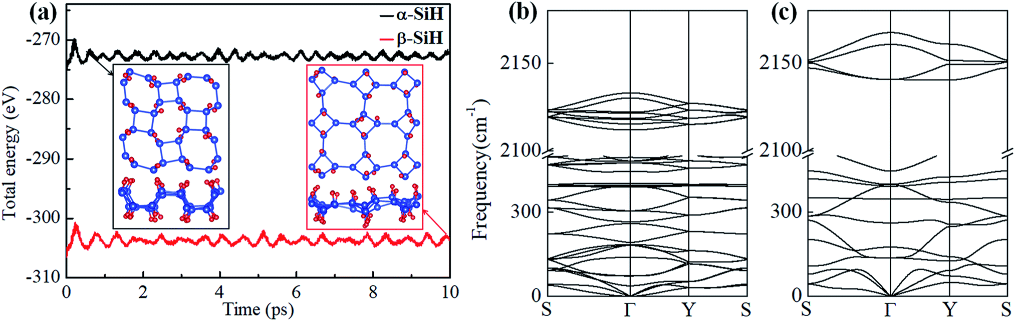 | ||
| Fig. 2 (a) Total energy fluctuations of α-SiH (black line) and β-SiH (red line) with respect to time in AIMD simulations at 300 K, the insets show the final structures at the end of 10 ps. Phonon dispersion of (b) α-SiH and (c) β-SiH. | ||
To study the effect of hydrogenation on the electronic structure of 2D tetragonal silicene, the electronic properties of α-, β- and γ-SiH with equilibrium lattice constant have been studied and band structures are displayed in Fig. 3. The results show that these three configurations are semiconductor with a direct band gap of 2.436 eV and 2.286 eV for α-SiH and γ-SiH, and indirect band gap of 2.414 eV for β-SiH. Thus, hydrogenation can effectively open the band gap of 2D tetragonal silicene and change it from a semimetal to a semiconductor. As shown in Fig. 3, the valence band maxima (VBM) of α-, β- and γ-SiH lies at Γ point, and the conduction band minima (CBM) of both α-SiH and γ-SiH lies at Γ point while the CBM occurs along the Γ–Y direction for β-SiH. By projecting the bands onto different atomic orbitals, it can be seen from Fig. 3 that the VBM is mostly consist of Si-pxy orbitals for three configurations, while the CBM is dominated by Si-pz orbitals for α-SiH and Si-s orbitals for both of β- and γ-SiH. The calculated band structure of γ-SiH is consistent with previous results reported by Wu et al.14 To verify the validity of the band gaps by PBE calculation, the HSE06 calculation is used to check the electronic band structure of those three systems. As shown in Fig. 4, the band gaps of α-SiH, β-SiH and γ-SiH at HSE06 calculation are increased to 3.244 eV, 3.177 eV and 3.090 eV, respectively, while the overall electronic band profiles calculated by PBE and HSE06 calculations are similar for three systems. The present work is mainly focused on the biaxial strain effect on the band structure of these three systems, although the band gaps are underestimated by PBE calculation, it is still be able to predict the general trends of strain effect on the band structures in α-SiH, β-SiH and γ-SiH.
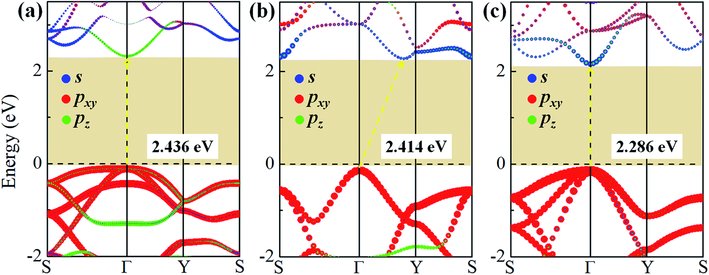 | ||
| Fig. 3 The projection electronic band structures of (a) α-SiH, (b) β-SiH and (c) γ-SiH, where the blue, red and green dots describe the contribution from s, pxy, and pz orbitals of Si atoms, respectively. The Fermi level is set to zero and denoted by a dashed line. | ||
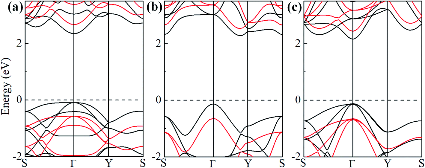 | ||
| Fig. 4 Band structures of (a) α-SiH, (b) β-SiH and (c) γ-SiH. The black and red lines in the band structures represent PBE and HSE06 calculations, respectively. The Fermi level is set to zero and denoted by a dashed line. | ||
It is well known that tailoring electronic properties of semiconductor materials is very critical for potential applications, strain engineering is one of the effective approaches to regulate the electronic properties of semiconductors. Here, we investigated the structural and electronic properties of α-, β- and γ-SiH under an external biaxial strain within the range of −10% to 12%. The biaxial strain is described as ε = (a − a0)/a0 × 100%, where a0 and a are the lattice constants of unstrained and strained systems, respectively. For the strained system, just atomic position is allowed to relax. Hereinto, strains in the range of −10% to 12% with spacing of 2% are considered, negative and positive values of strain ε refer to compressive and tensile strains, respectively. Fig. 5a gives the system energy, the variational ratio of bond lengths (l1, l2 and l3) and buckled height h0 as a function of biaxial strain. As seen in Fig. 5a, the energies increase with biaxial strain increases in a quadratic way for these three atomic configurations. The energy of β-SiH is larger than that of α-SiH and γ-SiH under different biaxial strains from −10% to 12%. The γ-SiH is energetically more stable than α-SiH with biaxial strain in the range of −2% ≤ ε ≤ 2%, while α-SiH is more stable than γ-SiH when biaxial strains exceed ±2%. The variational ratio of bond lengths and buckled height with respect to biaxial strain is displayed in Fig. 5b. The variational ratio of bond lengths and buckled height are defined as Δl = (Li − li)/li and Δh = (h − h0)/h0, respectively, where Li (i = 1, 2 and 3) and h signify the bond lengths and buckled height in strained system. For α-SiH system, it can be found that the variations of bond lengths l1 and l2 increase monotonously while bond length l3 is almost unchanged, and the buckled height h0 decreases monotonously for α-SiH under biaxial strain from −10% to 12%. The similar process can be found in the strained β-SiH and γ-SiH, just the variations in bond lengths l1 and l2 (buckled height h0) increase (decrease) more quickly.
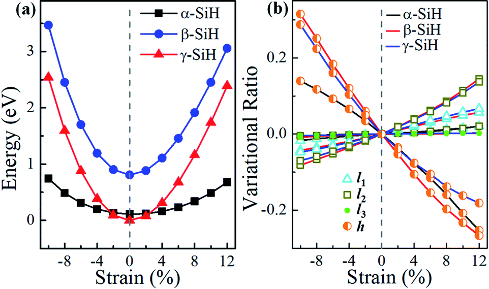 | ||
| Fig. 5 (a) System energy, (b) bond lengths and buckled height for α-SiH, β-SiH and γ-SiH as a function of biaxial strain. | ||
Now, we discuss the modulations of electronic band structures in α-, β- and γ-SiH by applying biaxial strain from −10% to 12%. The band gaps and band structures of three configurations under different strain are shown in Fig. 6 and 7, respectively. In Fig. 6, the band gap of α-SiH increases linearly within the tensile strain range from 0% to 12%, and it reduces under enhanced compressive strains in the range of 0% to −10%. As shown in Fig. 7a, there is a direct-to-indirect transition in α-SiH due to compressive strain, it shows an indirect band gap when the system is strained at −2%, where the location of the VBM lies along the S–Γ direction whereas the CMB remains at the Γ point. In the case of β-SiH, the band gap is reduced by applying either tensile or compressive strain as plotted in Fig. 6. It can be seen from Fig. 7b, the β-SiH can be transformed from an indirect character to direct character with both of the VBM and CBM lie at the S point, and the critical strain for indirect–direct transition is 12%. As seen in Fig. 6, the band gap of γ-SiH decreases with tensile strain increases whereas the band gap increases and then it decreases as the compressive strain increases, and the band gap of γ-SiH reaches a maximal value at −2% strain. When the compressive strain increases to −2%, the γ-SiH undergoes a transition from direct band gap to indirect band gap with its VMB still locating at Γ-point and CBM shifting from Γ point to a midpoint along S–Γ direction, as depicted in Fig. 7c.
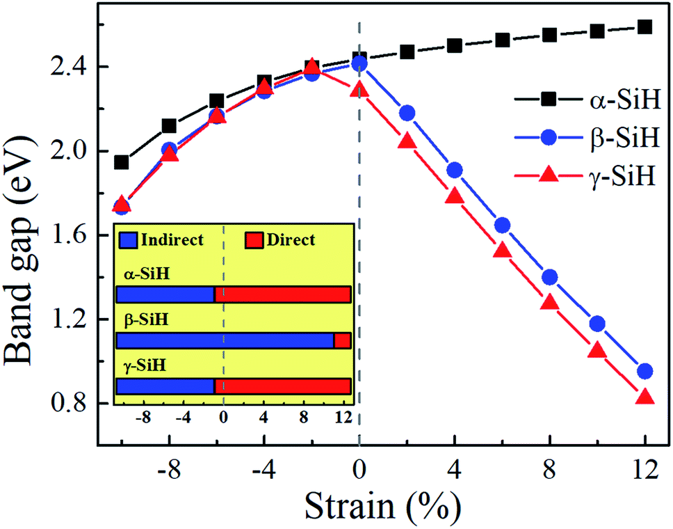 | ||
| Fig. 6 The Variation of band gap with respect to biaxial strain for α-SiH, β-SiH and γ-SiH. The insets show the schematic drawings of the gap type transition for three atomic configurations under the corresponding biaxial strain. The blue and red rectangles represent indirect and direct band gaps, respectively. | ||
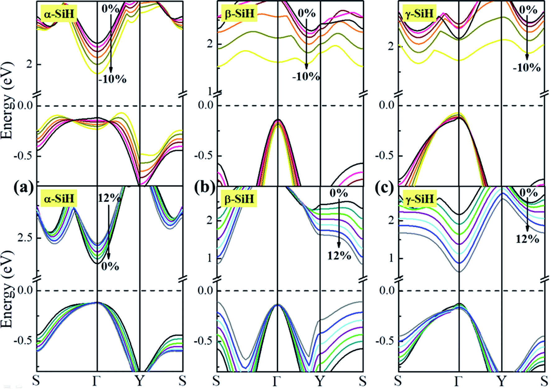 | ||
| Fig. 7 The band structures under different biaxial strain for (a) α-SiH, (b) β-SiH and (c) γ-SiH. The Fermi level is set to zero and denoted by a dashed line. | ||
4. Conclusions
In conclusion, in addition to the reported hydrogenated 2D tetragonal silicene (γ-SiH), the other two atomic configurations of hydrogenated 2D tetragonal silicene (α-SiH and β-SiH) have been proposed. The calculated binding energy, AIMD simulations and phonon dispersions indicate that both of α-SiH and β-SiH are stable. Both of them are semiconductors, the α-SiH has a direct band gap of 2.436 eV and β-SiH displays an indirect band gap of 2.286 eV. When applying external strain from −10% to 12%, the β-SiH is less stable than α-SiH and γ-SiH, γ-SiH is energetically more stable than α-SiH in the strain range of −2% ≤ ε ≤ 2% while α-SiH is more stable than γ-SiH when biaxial strains exceed ±2%. Furthermore, the electronic band structures and band gap type of α-SiH, β-SiH and γ-SiH can be effectively regulated by applying external biaxial strain. By means of biaxial strain, these three configurations experience direct–indirect or indirect–direct transition, and the band gap can be tuned in a range of 1.732–2.585 eV.Conflicts of interest
There are no conflicts to declare.Acknowledgements
This work was supported by the Specialized Fund for the Doctoral Research of Jilin Engineering Normal University under Grants No. BSKJ201904.References
- Z. Ni, Q. Liu, K. Tang, J. Zheng, J. Zhou, R. Qin, Z. Gao, D. Yu and J. Lu, Nano Lett., 2012, 12, 113–118 CrossRef CAS.
- H. Liu, J. Gao and J. Zhao, J. Phys. Chem. C, 2013, 117, 10353–10359 CrossRef CAS.
- C.-C. Liu, W. Feng and Y. Yao, Phys. Rev. Lett., 2011, 107, 076802 CrossRef.
- X. Li, J. T. Mullen, Z. Jin, K. M. Borysenko, M. Buongiorno Nardelli and K. W. Kim, Phys. Rev. B: Condens. Matter Mater. Phys., 2013, 87, 115418 CrossRef.
- B. Feng, Z. Ding, S. Meng, Y. Yao, X. He, P. Cheng, L. Chen and K. Wu, Nano Lett., 2012, 12, 3507–3511 CrossRef CAS PubMed.
- A. Fleurence, R. Friedlein, T. Ozaki, H. Kawai, Y. Wang and Y. Yamada-Takamura, Phys. Rev. Lett., 2012, 108, 245501 CrossRef PubMed.
- C. Grazianetti, E. Cinquanta and A. Molle, 2D Mater., 2016, 3, 012001 CrossRef.
- L. Meng, et al., Nano Lett., 2013, 13, 685–690 CrossRef CAS PubMed.
- F. Gimbert, C.-C. Lee, R. Friedlein, A. Fleurence, Y. Yamada-Takamura and T. Ozaki, Phys. Rev. B: Condens. Matter Mater. Phys., 2014, 90, 165423 CrossRef.
- M. Qiao, Y. Wang, Y. Li and Z. Chen, J. Phys. Chem. C, 2017, 121, 9627–9633 CrossRef CAS.
- S. Cahangirov, V. O. Özçelik, A. Rubio and S. Ciraci, Phys. Rev. B: Condens. Matter Mater. Phys., 2014, 90, 085426 CrossRef.
- S. Cahangirov, V. O. Özçelik, L. Xian, J. Avila, S. Cho, M. C. Asensio, S. Ciraci and A. Rubio, Phys. Rev. B: Condens. Matter Mater. Phys., 2014, 90, 035448 CrossRef.
- F. Matusalem, M. Marques, L. K. Teles and F. Bechstedt, Phys. Rev. B: Condens. Matter Mater. Phys., 2015, 92, 045436 CrossRef.
- H. Wu, Y. Qian, Z. Du, R. Zhu, E. Kan and K. Deng, Phys. Lett. A, 2017, 381, 3754–3759 CrossRef CAS.
- Z. Zhuo, X. Wu and J. Yang, Nanoscale, 2018, 10, 1265–1271 RSC.
- N. Jawad, J. Xue, P. Biswarup, Z. Jijun, K. Tae Won and A. Rajeev, Nanotechnol, 2012, 23, 385704 CrossRef PubMed.
- Y. Liu, G. Wang, Q. Huang, L. Guo and X. Chen, Phys. Rev. Lett., 2012, 108, 225505 CrossRef PubMed.
- C. Xu, Y. Wang, R. Han, H. Tu and Y. Yan, New J. Phys., 2019, 21, 033005 CrossRef CAS.
- K. Liangzhi, T. Xin, M. Yandong, T. Hassan, Z. Liujiang, S. Ziqi, A. Du, C. Changfeng and C. S. Sean, 2D Mater., 2015, 2, 045010 CrossRef.
- Y. Zhang, J. Lee, W.-L. Wang and D.-X. Yao, Comput. Mater. Sci., 2015, 110, 109–114 CrossRef CAS.
- Z. Zhu, X. Cai, C. Niu, C. Wang and Y. Jia, Appl. Phys. Lett., 2016, 109, 153107 CrossRef.
- C. Yang, Y. Xie, L.-M. Liu and Y. Chen, Phys. Chem. Chem. Phys., 2015, 17, 11211–11216 RSC.
- S. M. Nie, Z. Song, H. Weng and Z. Fang, Phys. Rev. B: Condens. Matter Mater. Phys., 2015, 91, 235434 CrossRef.
- A. M. van der Zande, P. Y. Huang, D. A. Chenet, T. C. Berkelbach, Y. You, G.-H. Lee, T. F. Heinz, D. R. Reichman, D. A. Muller and J. C. Hone, Nat. Mater., 2013, 12, 554 CrossRef CAS.
- C. Xu, J. Zhang, M. Guo and L. Wang, RSC Adv., 2019, 9, 23142–23147 RSC.
- J. Li, H. Li, Z. Wang and G. Zou, Appl. Phys. Lett., 2013, 102, 073114 CrossRef.
- A. Lopez-Bezanilla, P. Ganesh, P. R. C. Kent and B. G. Sumpter, Nano Res., 2014, 7, 63–70 CrossRef CAS.
- W. X. Zhang, H. Wang, C. H. Shi, S. Y. Liu, S. Y. Chang and C. He, J. Phys. Chem. C, 2019, 123, 14999–15008 CrossRef CAS.
- J. Zhou, Q. Wang, Q. Sun and P. Jena, Phys. Rev. B: Condens. Matter Mater. Phys., 2010, 81, 085442 CrossRef.
- Y. Ding and Y. Wang, J. Phys. Chem. C, 2018, 122, 23208–23216 CrossRef CAS.
- Y. Ding and Y. Wang, Appl. Phys. Lett., 2012, 100, 083102 CrossRef.
- X.-Q. Wang, H.-D. Li and J.-T. Wang, Phys. Chem. Chem. Phys., 2012, 14, 3031–3036 RSC.
- Y. Ding and Y. Wang, J. Mater. Chem. C, 2015, 3, 11341–11348 RSC.
- M. Houssa, E. Scalise, K. Sankaran, G. Pourtois, V. V. Afanas'ev and A. Stesmans, Appl. Phys. Lett., 2011, 98, 223107 CrossRef.
- J. Qiu, H. Fu, Y. Xu, A. I. Oreshkin, T. Shao, H. Li, S. Meng, L. Chen and K. Wu, Phys. Rev. Lett., 2015, 114, 126101 CrossRef PubMed.
- J. Qiu, H. Fu, Y. Xu, Q. Zhou, S. Meng, H. Li, L. Chen and K. Wu, ACS Nano, 2015, 9, 11192–11199 CrossRef CAS PubMed.
- W. Wang, W. Olovsson and R. I. G. Uhrberg, Phys. Rev. B, 2016, 93, 081406 CrossRef.
- D. Solonenko, V. Dzhagan, S. Cahangirov, C. Bacaksiz, H. Sahin, D. R. T. Zahn and P. Vogt, Phys. Rev. B, 2017, 96, 235423 CrossRef.
- D. B. Medina, E. Salomon, G. Le Lay and T. Angot, J. Electron Spectrosc. Relat. Phenom., 2017, 219, 57–62 CrossRef CAS.
- Y. Y. Hui, X. Liu, W. Jie, N. Y. Chan, J. Hao, Y.-T. Hsu, L.-J. Li, W. Guo and S. P. Lau, ACS Nano, 2013, 7, 7126–7131 CrossRef CAS PubMed.
- G. Plechinger, A. Castellanos-Gomez, M. Buscema, H. S. J. van der Zant, G. A. Steele, A. Kuc, T. Heine, C. Schüller and T. Korn, 2D Mater., 2015, 2, 015006 CrossRef.
- Y. Wang, C. Cong, W. Yang, J. Shang, N. Peimyoo, Y. Chen, J. Kang, J. Wang, W. Huang and T. Yu, Nano Res., 2015, 8, 2562–2572 CrossRef CAS.
- S. Yang, et al., Nano Lett., 2015, 15, 1660–1666 CrossRef CAS PubMed.
- A. Castellanos-Gomez, R. Roldán, E. Cappelluti, M. Buscema, F. Guinea, H. S. J. van der Zant and G. A. Steele, Nano Lett., 2013, 13, 5361–5366 CrossRef CAS PubMed.
- Y. Wang, C. Cong, R. Fei, W. Yang, Y. Chen, B. Cao, L. Yang and T. Yu, Nano Res., 2015, 8, 3944–3953 CrossRef CAS.
- Y. Li, Z. Hu, S. Lin, S. K. Lai, W. Ji and S. P. Lau, Adv. Funct. Mater., 2017, 27, 1600986 CrossRef.
- N. Wu, X. Zhao, X. Ma, Q. Xin, X. Liu, T. Wang and S. Wei, Phys. E, 2017, 93, 1–5 CrossRef CAS.
- H. Shu, X. Niu, X. Ding and Y. Wang, Appl. Surf. Sci., 2019, 479, 475–481 CrossRef CAS.
- Q.-Y. Chen, C. Cao and Y. He, Phys. E, 2019, 113, 172–180 CrossRef CAS.
- F. Ersan, Comput. Mater. Sci., 2019, 163, 278–281 CrossRef CAS.
- G. Kresse and J. Furthmüller, Phys. Rev. B: Condens. Matter Mater. Phys., 1996, 54, 11169–11186 CrossRef CAS.
- G. Kresse and J. Hafner, Phys. Rev. B: Condens. Matter Mater. Phys., 1993, 47, 558–561 CrossRef CAS.
- G. Kresse and J. Hafner, Phys. Rev. B: Condens. Matter Mater. Phys., 1994, 49, 14251–14269 CrossRef CAS.
- P. E. Blöchl, Phys. Rev. B: Condens. Matter Mater. Phys., 1994, 50, 17953–17979 CrossRef.
- J. P. Perdew, K. Burke and M. Ernzerhof, Phys. Rev. Lett., 1996, 77, 3865–3868 CrossRef CAS.
- J. Heyd, G. E. Scuseria and M. Ernzerhof, J. Chem. Phys., 2003, 118, 8207–8215 CrossRef CAS.
- D. Alfè, Comput. Phys. Commun., 2009, 180, 2622–2633 CrossRef.
- D. B. Putungan, S.-H. Lin and J.-L. Kuo, Phys. Chem. Chem. Phys., 2015, 17, 21702–21708 RSC.
- S.-Y. Chen, C. H. Naylor, T. Goldstein, A. T. C. Johnson and J. Yan, ACS Nano, 2017, 11, 814–820 CrossRef CAS PubMed.
- G. H. Han, et al., 2D Mater., 2016, 3, 031010 CrossRef.
- J. Lee, F. Ye, Z. Wang, R. Yang, J. Hu, Z. Mao, J. Wei and P. X. L. Feng, Nanoscale, 2016, 8, 7854–7860 RSC.
- A. P. Nayak, et al., Nano Lett., 2015, 15, 346–353 CrossRef CAS.
- Q. Song, H. Wang, X. Pan, X. Xu, Y. Wang, Y. Li, F. Song, X. Wan, Y. Ye and L. Dai, Sci. Rep., 2017, 7, 1758 CrossRef PubMed.
| This journal is © The Royal Society of Chemistry 2019 |