
 Open Access Article
 This Open Access Article is licensed under a Creative Commons Attribution-Non Commercial 3.0 Unported Licence
Effects of NaCl treatment on the performance and environmental stability of microporous SiO2-based thin film transistors
Wei Dou *a and
Yuanyuan Tanb
*a and
Yuanyuan Tanb
aKey Laboratory of Low Dimensional Quantum Structures and Quantum Control, School of Physics and Electronics, Hunan Normal University, Changsha, 410081, People's Republic of China. E-mail: douwei139@163.com
bHunan First Normal University, Changsha, 410205, People's Republic of China
First published on 15th November 2019
Abstract
In this letter, we report the effects of NaCl treatment on the performance and environmental stability of microporous SiO2-based thin film transistors (TFTs). It was found that appropriate amounts of NaCl treatment significantly improved the electric double layer (EDL) capacitance of such composite solid electrolytes from 1.9 to 4.7 μF cm−2. A highest field effect mobility of 42.8 cm2 V−1 s−1 was found for 1% NaCl treated microporous SiO2-based TFTs. However, 10% and 26.5% NaCl treated microporous SiO2-based TFTs showed good environmental stability of the Ion/Ioff ratio with reasonable field effect mobility.
Introduction
Microporous SiO2-based thin film transistors (TFTs) have attracted much attention in recent years due to their superior performance compared to the common SiO2-based TFTs. Microporous SiO2 dielectrics have several advantages such as high specific capacitance, good environmental stability in ambient air and simple deposition methods at room temperature. Various SiO2-based TFTs have been reported in recent years.1–5 The enhancement of the electric double layer (EDL) capacitance of SiO2 dielectrics strongly influences the performance of SiO2-based TFTs.1–3 The EDL capacitance of microporous SiO2 dielectrics can be enhanced either by reducing the thickness of the SiO2 film or by ionic treatment. It has been reported that microporous SiO2 with appropriate amounts of LiCl and/or CaCl2 treatment effectively enhanced the EDL capacitance of microporous SiO2 dielectrics.4,5For practical applications, the environmental stability of microporous SiO2-based TFTs should be considered. The environmental stability of field-effect mobility of 1% CaCl2 treated microporous SiO2-based TFTs has been reported.5 However, the information on the stability of on/off ratio of the TFTs which is an important factor for switching applications has been rarely mentioned. In this letter, we report the effect of NaCl treatment on the performance and environmental stability of microporous SiO2-based TFTs.
Experimental
The entire process of the microporous SiO2-based TFTs fabrication was performed at room temperature. First of all, microporous SiO2 gate dielectric with the thickness of 2 μm was deposited by plasma-enhanced chemical vapor deposition (PECVD) method on ITO glass and Si (100) substrates using SiH4 and O2 mixture as the reactive gases. Then, the samples were immersed in 0.1%, 1%, 10% and 26.5% NaCl aqueous solution, respectively. After 3 hours, these samples were taken out and dried in air ambient. Then, a 40 nm-thick ITO layer was deposited by RF magnetron sputtering method with a RF power of 100 W in Ar/O2 (4![[thin space (1/6-em)]](https://www.rsc.org/images/entities/char_2009.gif) :1) mixed ambient of 0.5 Pa as active channel. At last, highly conductive ITO layers were deposited by dc sputtering methods in pure argon ambient at 1.0 Pa as source and drain electrodes. The channel length and width-to-length ratio of the shadow mask were 80 μm and 12.5:1, respectively. The structural characterization of the microporous SiO2 electrolyte film was investigated by field emission scanning electron microscopy (Hitachi S-4800 SEM). The electrical characterizations of the microporous SiO2 dielectric and EDL transistors were investigated by an impedance analyzer (WK 6500B) and a semiconductor parameter analyzer (Keithley 4200 SCS) at room temperature in dark with a relative humidity of 60%.
:1) mixed ambient of 0.5 Pa as active channel. At last, highly conductive ITO layers were deposited by dc sputtering methods in pure argon ambient at 1.0 Pa as source and drain electrodes. The channel length and width-to-length ratio of the shadow mask were 80 μm and 12.5:1, respectively. The structural characterization of the microporous SiO2 electrolyte film was investigated by field emission scanning electron microscopy (Hitachi S-4800 SEM). The electrical characterizations of the microporous SiO2 dielectric and EDL transistors were investigated by an impedance analyzer (WK 6500B) and a semiconductor parameter analyzer (Keithley 4200 SCS) at room temperature in dark with a relative humidity of 60%.
Results and discussion
Fig. 1(a) shows the schematic picture of ITO-based TFTs gated by microporous SiO2 treated by NaCl. On account of immersing into NaCl aqueous solution for 3 hours, some protons enter the microporous SiO2 and some anions adhere to the surface of the microporous SiO2, these anions induce image charges of equal density and opposite sign in the dielectric layer, which is similar to the case of EDL organic transistors gated by ionic liquids or solid state electrolytes.6,7 Its transformation may be driven by proton transfer to and from a water molecule with very little permittivity temperature dependence.8–11 The major advantage of the EDL effect is that the specific capacitance is exceptionally large which results in an ultrahigh current throughput at an ultralow operating voltage of 0.5 V. Fig. 1(b) shows the density dependence of the specific capacitance versus frequency of the microporous SiO2 with and without NaCl treatment in the frequency range from 20 Hz to 5 MHz. Compared with the SiO2 without NaCl treatment, the specific capacitance of microporous SiO2 with 10% and 26.5% NaCl treatment has increased to 4.7 μF cm−2 at 20 Hz and remains about 1 μF cm−2 at 1 kHz. However, the specific capacitance of microporous SiO2 with 1% NaCl treatment is about 2 μF cm−2 and decreases rapidly. It is expected that this behavior is mainly due to the changing of Na+ ions concentration in the films, which is similar to the incorporation of Na+ ions into gate dielectrics.12–14 The out-put characteristics of all the TFTs with and without NaCl treatment showed typical transistor behavior. Fig. 2 shows the transfer characteristics of the TFTs with and without NaCl treatment measured after different time interval of fabrication. The fresh measurement refers to the TFTs fabrication after 3 h of SiO2 film deposition and the electrical properties were measured within 1 h of the device fabrication. To study the environmental stability of the TFTs with and without NaCl treatment, the devices were exposed to air without surface passivation and their electrical properties were measured after 1 week and 1 month of device fabrication. The saturation field effect mobility (μsat) was extracted by fitting a straight line to the plot of the square root of the drain current versus Vgs, on the basis of the following relationship in the saturation regime, Ids = (W/2L)μsatCi(Vgs − Vth)2, where Ids is the drain current, Vth is the threshold voltage, W and L are the channel width and length, respectively, and Ci is the capacitance per unit area of the gate dielectric. The large mobilities of depletion mode (Vth = −0.17 to −0.35 V) TFTs probably derive from the high charge density in the channel, because the carrier mobility in polymer semiconductors is strongly dependent on carrier density, which result in increased trap filling and a general smoothing of electrostatic potential variations in the film due to trapped charge, these combined effects lead to higher carrier mobilities.15,16 The electrical parameters of the TFTs are listed in Table 1. The mobility and Ion/Ioff ratio of the drain current for the freshly prepared TFT without NaCl treatment were 12 cm2 V−1 s−1 and 3.4 × 10⁵, respectively. The threshold voltage (Vth) was −0.1 V and it was shifted in the positive direction with exposure to air. The Ion/Ioff ratio of the TFT without NaCl treatment measured after 1 week and 1 month of air exposure were 1.8 × 10⁵ and 6 × 10⁴, respectively. The mobility was significantly decreased with exposure to air. The TFT with 1% NaCl treatment showed a mobility of 41.8 cm2 V−1 s−1 and the mobility was decreased to 15 cm2 V−1 s−1 with an Ion/Ioff ratio of 3.1 × 10⁶ after 1 week aging. From Table 1 it is noted that after 1 month aging the TFT with 1% NaCl treatment showed a lower stability than the TFT without NaCl treatment. The mobility and Ion/Ioff ratio for the freshly prepared TFT with 10% NaCl treatment was 64.5 cm2 V−1 s−1 and 2.5 × 10⁶, respectively. In this case, the mobility was decreased to 29.3 and 12 cm2 V−1 s−1 after 1 week and 1 month aging, respectively. The TFT with 26.5% NaCl treatment showed a mobility and Ion/Ioff ratio of 36.5 cm2 V−1 s−1 and 3.5 × 10⁶, respectively, and the Ion/Ioff ratio measured after 1 month aging was 1.2 × 10⁷, which is about three orders of magnitude higher than the Ion/Ioff ratio of TFT without NaCl treatment. It is noted that, the threshold voltage of the TFTs was shifted in positive direction after 1 month aging, which may be attributed to the reduction of defect or trap density at the gate dielectric and channel interface.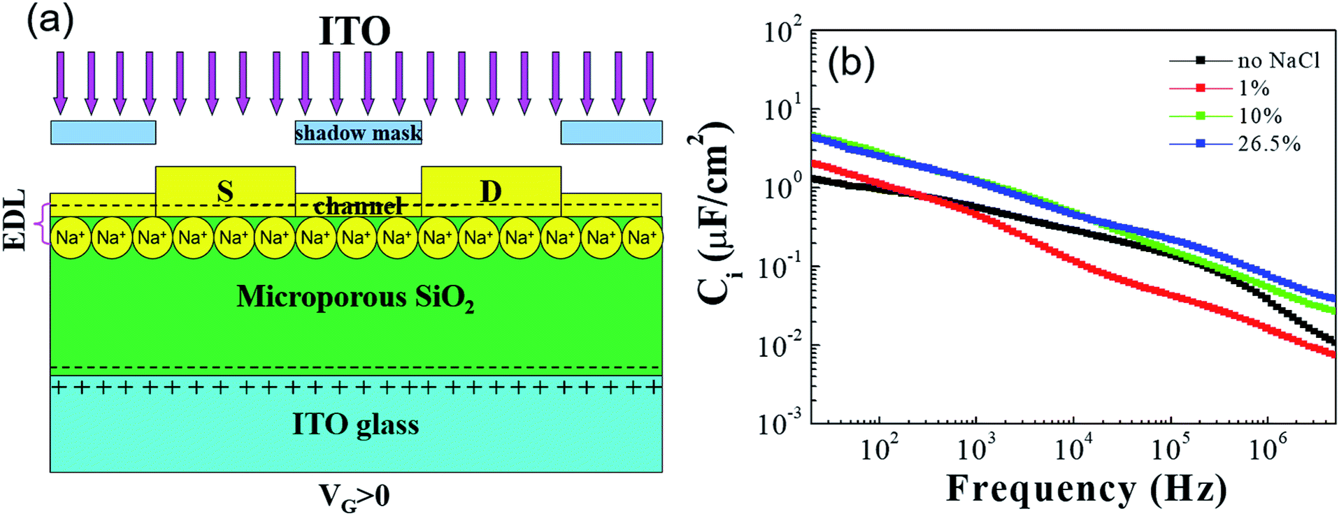 | ||
| Fig. 1 (a) Schematic picture of ITO-based TFTs gated by microporous SiO2 treated by NaCl. (b) Density dependence of the specific capacitance versus frequency of the microporous SiO2 with and without NaCl treatment in the frequency. | ||
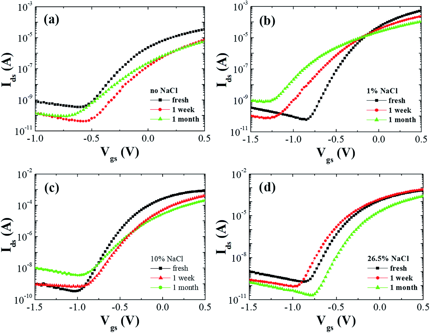 | ||
| Fig. 2 Transfer characteristics of TFTs (a) without and with (b) 1%, (c) 10% and (d) 26.5% NaCl treatment measured after different durations of air exposure. | ||
| NaCl content | Fresh | 1 week aging | 1 month aging | |||||||||
|---|---|---|---|---|---|---|---|---|---|---|---|---|
| μ (cm2 V−1 s−1) | Ion/Ioff | Vth (V) | S (mV per decade) | μ (cm2 V−1 s−1) | Ion/Ioff | Vth (V) | S (mV per decade) | μ (cm2 V−1 s−1) | Ion/Ioff | Vth (V) | S (mV per decade) | |
| 0 | 12 | 3.4 × 10⁵ | −0.1 | 110 | 4.3 | 1.8 × 10⁵ | 0.04 | 120 | 3.6 | 6 × 10⁴ | 0.05 | 180 |
| 1% | 41.8 | 1.1 × 10⁷ | −0.2 | 100 | 15 | 3.1 × 10⁶ | −0.28 | 150 | 5.7 | 1.3 × 10⁵ | −0.35 | 160 |
| 10% | 64.5 | 2.5 × 10⁶ | −0.17 | 100 | 29.3 | 7 × 10⁵ | −0.2 | 130 | 12 | 6 × 10⁴ | −0.11 | 180 |
| 26.5% | 32.6 | 3.5 × 10⁶ | −0.35 | 90 | 36.5 | 9.2 × 10⁶ | −0.37 | 90 | 24 | 1.2 × 10⁷ | −0.16 | 90 |
To understand the effect of air exposure on the stability of the TFTs, the subthreshold slope was calculated using the following function: S = δVgs/(δlog10Ids). From Table 1, it is clearly seen that the subthreshold slope rapidly increased with air exposure duration in case of the TFT without NaCl treatment and a moderate increase of subthreshold slope was also observed for the TFTs with 1% and 10% NaCl treatment. However, almost constant subthreshold slope was observed for the TFTs with 26.5% NaCl treatment.
In order to further investigate the stability and reproducibility of the TFTs with and without NaCl treatment, the bias stress measurements have been performed. Fig. 3 shows the bias stress curves for transistors gated by microporous SiO2 with and without NaCl treatment. After 10 minutes bias with Vgs = 0.5 V and Vds = 0.5 V, transistor gated by 26.5% NaCl-treated microporous SiO2 shows a small on current loss of 1.7%. While the transistor gated by microporous SiO2 without NaCl treatment shows an on current loss of 9.3%. For dynamic stress test (inset in Fig. 3), the transistor was repeatedly cycled between on and off states (period square wave pulses of Vgs = +0 V to −1.0 V and Vds = 0.5 V). TFT gated by NaCl-treated microporous SiO2 maintained a current on/off ratio of 106 and without obvious current degradation after more than 2000 seconds operation. These results suggest that no chemical doping (i.e. Na+ penetrate into the ITO channel) or chemical reaction occurs at the electrolyte/ITO channel interface when the gate potential is biased. As we know, if chemical doping or a chemical reaction occurs, Ids will not return to its original value after gate scanning.17
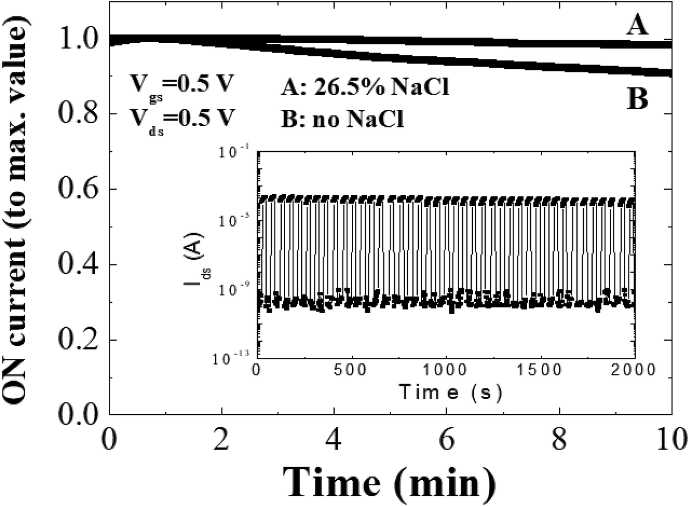 | ||
| Fig. 3 Normalized ON current (Ids) measured versus time for EDL TFTs gated by microporous SiO2 with and without NaCl treatment. Inset shows the dynamic stress test of the TFTs gated by 26.5% NaCl-treated microporous SiO2. | ||
Conclusions
In conclusion, we have investigated the effects of NaCl treatment on the performance and environmental stability of microporous SiO2-based TFTs. The results showed that an appropriate amount of NaCl treatment can enhance the EDL capacitance of the microporous SiO2 dielectric, which are the key factors for obtaining high performance TFTs. Further, with an optimized amount of NaCl treatment, the environmental stability of Ion/Ioff ratio and on current of the NaCl treated microporous SiO2-based TFTs can be improved with a reasonable field effect mobility which is very important for switching applications.Conflicts of interest
There are no conflicts to declare.Notes and references
- L. Kong, J. Sun, C. Qian, G. Gou, Y. He, J. Yang and Y. Gao, Org. Electron., 2016, 39, 64 CrossRef CAS.
- X. Hu, J. Sun, C. Qian, F. Liu, J. Yang, G. Guo and Y. Gao, J. Mater. Chem. C, 2016, 4, 150 RSC.
- J. Sun, W. Huang, C. Qian, J. Yang and Y. Gao, Phys. Chem. Chem. Phys., 2014, 16, 1084 RSC.
- J. Jiang, J. Sun, B. Zhou, A. Lu and Q. Wan, Appl. Phys. Lett., 2010, 97, 052104 CrossRef.
- W. Dou, J. Sun, J. Jiang, A. Lu and Q. Wan, Jpn. J. Appl. Phys., 2010, 49, 110201 CrossRef.
- T. Uemura, M. Yamagishi, S. Ono and J. Takeya, Appl. Phys. Lett., 2009, 95, 103301 CrossRef.
- B. N. Pal, B. M. Dhar, K. C. See and H. E. Katz, Nat. Mater., 2009, 8, 898 CrossRef CAS PubMed.
- Y. F. Chang, B. Fowler, Y. C. Chen, Y. T. Chen, Y. Wang, F. Xue, F. Zhou and J. C. Lee, J. Appl. Phys., 2014, 116, 043708 CrossRef.
- Y. F. Chang, B. Fowler, Y. C. Chen, Y. T. Chen, Y. Wang, F. Xue, F. Zhou and J. C. Lee, J. Appl. Phys., 2014, 116, 043709 CrossRef.
- E. Terzini, P. Thilakan and C. Minarini, Mater. Sci. Eng., B, 2000, 77, 110 CrossRef.
- Y. Wang, B. Fowler, F. Zhou, Y. F. Chang, Y. T. Chen, F. Xue and J. C. Lee, Appl. Phys. Lett., 2013, 103, 213505 CrossRef.
- J. M. Schneider, B. Hjorvarsson, X. Wang and L. Hultman, Appl. Phys. Lett., 1999, 75, 3476 CrossRef CAS.
- P. Gonon and F. E. Kamel, Appl. Phys. Lett., 2007, 90, 232902 CrossRef.
- J. A. Theil, D. V. Tsu, M. W. Watkins, S. S. Kim and G. Lucovsky, J. Vac. Sci. Technol., A, 1990, 8, 1374 CrossRef CAS.
- M. C. J. M. Vissenberg and M. Matters, Phys. Rev. B: Condens. Matter Mater. Phys., 1998, 57, 12964 CrossRef CAS.
- C. Tanase, E. J. Meijer, P. W. M. Blom and D. M. de Leeuw, Phys. Rev. Lett., 2003, 91, 216601 CrossRef CAS PubMed.
- L. Herlogsson, X. Crispin, N. D. Robinson, M. Sandberg, O. J. Hagel, G. Gustafsson and M. Berggren, Adv. Mater., 2007, 19, 97 CrossRef CAS.
| This journal is © The Royal Society of Chemistry 2019 |