
 Open Access Article
 This Open Access Article is licensed under a Creative Commons Attribution-Non Commercial 3.0 Unported Licence
Effects of 1,2-ethanedithiol concentration on performance improvement of quantum-dot LEDs†
Huu Tuan Nguyen‡
 *ab,
Shin Young Ryu‡c,
Anh Tuan Duongab and
Soonil Lee*c
*ab,
Shin Young Ryu‡c,
Anh Tuan Duongab and
Soonil Lee*c
aPhenikaa Research and Technology Institute (PRATI), A&A Green Phoenix Group, 167 Hoang Ngan, Hanoi 10000, Viet Nam. E-mail: tuan.nguyenhuu@phenikaa-uni.edu.vn
bFaculty of Electrical and Electronic Engineering, Phenikaa Institute for Advanced Study (PIAS), Phenikaa University, Yen Nghia, Ha-Dong District, Hanoi 10000, Viet Nam
cDepartment of Physics, Department of Energy Systems Research, Ajou University, Suwon 16499, Republic of Korea. E-mail: soonil@ajou.ac.kr
First published on 25th November 2019
Abstract
We report systematic efficiency variations of green-emitting CdSe@ZnS quantum-dot (QD) LEDs (QLEDs) in response to in situ treatments with 1,2-ethanedithiol (EDT) solutions at various concentrations. The main effect of in situ EDT treatment on a QD layer spin-coated onto a ZnO layer was vacuum-level shift due to dipole moments on the surface of the QD layer and at the interface between QD and ZnO layers. Competing contributions of these dipole moments were responsible for changes in energy level configurations and, accordingly, electron and hole barriers that resulted in discrepancies in electron- and hole-current variations. QLED efficiency was best when treated with an EDT solution of 4 mM, attributable to the largest increase in the hole- to electron current ratio. The maximum luminous yield of the 4 mM EDT-treated QLED was 5.43 cd A−1, which is 10 times higher than that of an untreated device. Furthermore, the luminous yield of this treated device remained as high as 2.56 cd A−1 at a luminance of 500 cd m−2.
1 Introduction
Colloidal quantum dots (QDs) are an emerging class of tunable semiconductor materials with unique and useful characteristics such as high photoluminescence (PL) quantum yield (QY), high color purity, and intrinsic compatibility with solution processes. Such traits have made colloidal QDs particularly promising candidates for next-generation displays and lighting systems, thus motivating many studies.1–9 To this end, extensive efforts have been made to improve QD LED (QLED) performance toward the goal of simultaneously achieving high brightness, efficiency and durability.The first step in improving the performance of QD devices, such as QLEDs and QD solar cells (QSCs) is the fabrication of QD active layers with sufficiently low defect concentrations to minimize defect states that can hinder charge-carrier transport and/or cause charge-carrier recombination. The quality of colloidal QDs is known to depend critically on the length and chemical structure of surface-ligand molecules. During a typical QD synthesis process, defect states can easily form because of incomplete defect passivation, leading to significantly low external quantum efficiency (EQE) for QLEDs and QSCs.10,11 Therefore, the choice of optimal ligand molecules for surface passivation is essential for the production of high-performance QLED and QSC devices. Indeed, the utilization of high conductive molecules as a substitute for insulating ligands has emerged as a new trend in QLED and QSC research.12–19
In this work, we fabricated and characterized green-color emitting QLEDs that had a CdSe@ZnS-QD EML, a ZnO electron transport layer (ETL) and a BCP hole transport layer (HTL). In spite of combing a ZnO ETL and a BCP HTL, each known for its high charge-carrier mobility, the efficiency of pristine QLEDs was low20,21 because CdSe@ZnS QDs were originally capped with oleic acid (OA) ligands.22,23 However, when we treated QD EMLs with a EDT solution to exchange long OA ligands with short and more conductive EDT ligands, efficiency improved dramatically. To maximize efficiency improvement resulted from EDT treatment and to elucidate efficiency-improvement mechanism in detail, we investigated EDT concentration dependence of QLED-efficiency improvement. Moreover, we analyzed QLED operation characteristics by representing measured currents as the sum of two modified Shockley functions for imperfect diodes,24 each corresponding to electron or hole currents.
Solid-phase in situ ligand exchange is of particular interest because of its simplicity and potential for cost reduction in mass production and commercialization stages.17,25,26 Moreover, ligand exchange with EDT molecules is interesting for its contribution to the fundamental mechanism of OLED operation. EDT molecules are known to induce vacuum level shift due to their dipole moments.7,25–28 Consequently, EDT treatment is expected to alter the relative positions of the lowest unoccupied molecular orbital (LUMO) and highest occupied molecular orbital (HOMO) of charge transport layers and a QD emitting layer (EML) without changing LUMO–HOMO gap.27,29 HOMO and LUMO variations in QLED devices can lead to modification of electron- and hole-barriers and, accordingly, changes in electron and hole currents.
2 Experimental section
QLED devices were fabricated to have an inverted architecture of ITO/ZnO/QD/CBP/MoO3/Al. A 140 nm-thick ITO layer with sheet-resistance of 9 Ω sq−1 was the transparent cathode, a 50 nm-thick ZnO layer was the ETL, a green-emitting QD layer was the EML, a 40 nm-thick CBP layer was the HTL, a 10 nm-thick molybdenum oxide (MoO3) was the hole injection layer (HIL), and a 100 nm-thick aluminum (Al) was the anode. The ZnO ETL was made from a solution of ZnO nanoparticles (NPs) in 1-butanol, and the QD EML from a colloidal solution of CdSe@ZnS QDs in ethanol, that has chemical-composition gradient and PL QY of 75%. The details of ZnO-NP and CdSe@ZnS-QDs synthesis were previously reported.29For the device fabrication process, a piece of ITO glass was first thoroughly cleaned, and the ITO layer was patterned into a cathode.30,31 Second, a ZnO-NP solution was spin-coated onto a plasma-treated ITO cathode to form an ETL. Before the deposition of subsequent QD and organic layers, the ITO-glass substrate coated with ZnO NPs was loaded into a glove box and baked at 90 °C for 30 min to eliminate any residual solvents. Next, a QD EML was spin-coated from a 6 mg ml−1 solution of colloidal CdSe@ZnS QDs in toluene. For in situ EDT treatments, each QD EMLs were fully covered with several drops of the acetonitrile solutions of EDT at respective concentrations of 3, 4 and 6 mM. After waiting for 40 seconds, excess EDT and OA were removed by spin-drying at 4000 rpm for 30 seconds. All of these processes were conducted inside a N2 glove box. Finally, a CBP HTL and a MoO3/Al anode were deposited by thermal evaporation at vacuum of 3 × 10⁻⁶ torr. The growth rates for both CBP and Al were 1 Å s−1 and that for MoO3 was 0.1 Å s−1. The area of square pixel of fabricated devices, defined by the anode–cathode overlap, was 3 × 3 mm2. All fabricated devices were hermetically sealed prior to measurement by glass encapsulation with enclosed getter. QLED devices fabricated with EDT treatment at 3, 4 and 6 mM were named as devices E3-, E4-, and E6-QLED, respectively. A control device fabricated without EDT treatment was designated as P-QLED.
A computer-controlled Keithley 236 source-measurement unit was used to measure currents with respect to bias voltages, and a Minolta CS-100A was used for concomitant luminance measurement. Electroluminescence (EL) and PL spectra were measured with a Darsa Pro-5000 System and an F-7000 spectrofluorometer, respectively.
3 Results and discussion
Current density versus voltage (J–V) characteristics of a series of QLEDs that were treated with acetonitrile solutions of EDT at various concentrations are compared in Fig. 1(a). J–V curves show a systematic decrease in current densities in response to increase in EDT concentrations. All the QLEDs share similar features in J–V characteristic as the log-scale plots of J versus V in Fig. S1† show: current onset at around 1 V, exponential increase of J with respect to V, and appearance of a voltage-drop effect due to a series resistance at high bias voltages. Current densities increase four orders of magnitude up to 6 V, and 10–30 times more up to the maximum measured bias ranges of 9–11 V. However, luminance versus voltage (L–V) characteristics are not uniformly dependent on EDT-concentrations as shown in Fig. 1(b). Initially, luminance increased slightly after treatment with a 3 mM EDT solution and more prominent luminance increase resulted from the 4 mM EDT treatment. However, the use of 6 mM EDT solution for EDT treatment resulted in luminance decrease.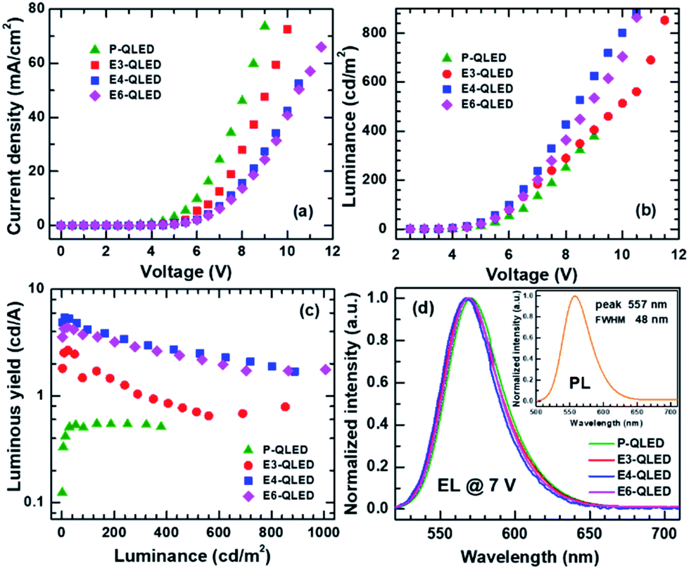 | ||
| Fig. 1 Variations of (a) current density J and luminance L (b) with respect to voltage V, and luminous yield with respect to luminance (c). Comparison of electroluminescence spectra of the device P-, E3-, E4 and E6-QLED (d). Inset shows photoluminescence spectrum of colloidal CdSe@ZnS quantum dots. | ||
Luminance increase concurrent with current–density decrease indicates that EDT treatment is an effective method for the improvement of efficiency of QLED devices. The maximum luminous yield of the device P-QLED was only 0.549 cd A−1, but those of the devices E3-, E4-, and E6-QLED were 2.68, 5.43, and 4.41 cd A−1, respectively (see Fig. 1(c)). Moreover, luminous yields at 500 cd m−2 were 0.723, 2.56, and 2.37 cd A−1 for the devices E3-, E4-, and E6-QLED, respectively. We note that efficiency improvement of QLED devices in response to EDT treatment was achieved without noticeable change in emission color as shown in Fig. 1(d). Emission from the P-QLED device peaked at 570 nm with a full width at half maximum (FWHM) of 42 nm. Interestingly, all electroluminescence (EL) spectra of the EDT-treated devices look similar. The device E3-QLED show a EL peak at 568 nm with FWHM of 43 nm, while EL peaks of devices E4- and E6-QLED appear at 567 and 569 nm with the identical FWHM of 41 nm. These EL spectra are similar to a PL spectrum of colloidal CdSe@ZnS QDs in the inset of Fig. 1(d): a peak at 557 nm with 48 nm FWHM.
Resemblance of the EL spectra to the PL spectrum of colloidal QDs indicate that electron–hole recombination which results in green-light emission occurred exclusively within respective QD EMLs of the QLED devices. Therefore, aforementioned changes of J–V and L–V characteristics with respect to EDT concentrations are expected to be accounted by variations in electron and hole flows towards QD EMLs. In this work, we modeled the J–V characteristics in a diffusion-dominant range as the sum of two diode currents that correspond to majority- and minority-carrier currents, respectively. Specifically, we used a modified Shockley equation that took into account voltage drop due to a series resistance for phenomenological representation of each current.24
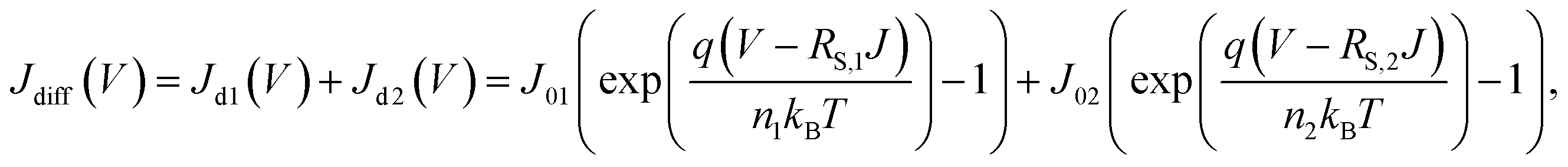 | (1) |
Fig. 2 shows the fitting results of measured J–V curves in a diffusion-dominant range to the two-diode model in eqn (1). The parameter values corresponding to the fitting curves Jd1 and Jd2 are summarized in Table 1. Good agreement between the measured and calculated J–V curves by using the fitting parameters in Table 1 indicates that our phenomenological representation of the J–V characteristics is a useful approach to elucidate discrepancy in QLED operation with respect to EDT concentrations used for a ligand-exchange process.
 | ||
| Fig. 2 Comparison of measured and fitted J–V curves of the device P-, E3-, E4-, and E6-QLED. Fitting to a phenomenological model that consists of two diode currents produced good agreement between measured and calculated J–V curves. | ||
| Components | Parameters | Sample ID | |||
|---|---|---|---|---|---|
| P-QLED | E3-QLED | E4-QLED | E6-QLED | ||
| Diode 1 | n1 | 25.0 ± 0.7 | 21.8 ± 0.3 | 20.9 ± 0.5 | 22.0 ± 0.7 |
| J0,1 (mA cm−2) | (1.30 ± 0.27) × 10−6 | (9.32 ± 1.36) × 10−8 | (2.30 ± 0.50) × 10−8 | (3.16 ± 1.01) × 10−8 | |
| RS,1 (Ω cm2) | 27.1 ± 1.1 | 33.6 ± 0.7 | 55.9 ± 1.9 | 55.5 ± 3.2 | |
| Diode 2 | n2 | 16.2 ± 1.0 | 15.8 ± 1.1 | 15.8 ± 0.8 | 15.4 ± 0.6 |
| J0,2 (mA cm−2) | (6.31 ± 5.10) × 10−10 | (1.76 ± 1.50) × 10−9 | (1.32 ± 0.83) × 10−9 | (6.41 ± 3.35) × 10−10 | |
| RS,2 (Ω cm2) | 645.1 ± 29.9 | 754.0 ± 17.8 | 443.4 ± 9.6 | 504.7 ± 8.7 | |
A large ideality factor in a Shockley equation is linked to charge-carrier loss due to recombination, leakage, trap-assisted tunneling, and/or inhomogeneous junctions. Accordingly, we argue that larger values of n1 is a signature for more prominent contribution of defects to majority-carrier currents, and that the decrease of n1 from 25 to 20–22 after EDT treatment is indicative of defect passivation by EDT molecules to result in less majority-carrier loss. In contrast, n2 shows only a slight difference from 16.2 for the device P-QLED to 15.4 for the E6-QLED, which suggests that both defect-related loss and defect-passivation effects are less significant for minority carriers. Smaller RS,1 and an increase in RS,1 from 27 Ω cm2 for the P-QLED to 56 Ω cm2 for the E4-QLED can be a collaborating evidence for majority-carrier loss through defect states and defect passivation by EDT molecules. In the case of minority-carrier currents RS,2 is one order of magnitude larger regardless of EDT treatment, which is consistent with less contributions of defect states to minority-carrier loss. Another prominent discrepancy appears in reverse saturation currents. For example, J0,1 of the P-QLED was initially as large as 1.30 × 10⁻⁶ mA cm−2, which is 2000 times larger than J0,2, but J0,1 was reduced by 1 or 2 orders of magnitude with EDT treatment. On the contrary, J0,2 increased by a factor of 2–3 for the devices E3- and E4-QLED, but remained at the initial level for the device E6-QLED.
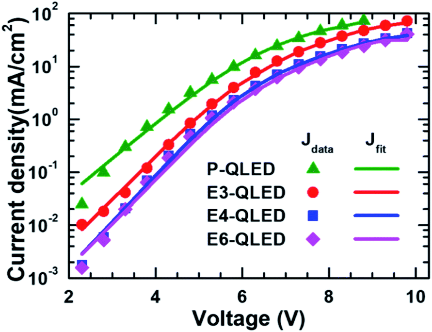
We compared majority- (Jd1) and minority-carrier current densities (Jd2) of each device, which were estimated using the respective fitting parameters in Fig. 3. The main features are dominant contributions of Jd1 to measured J–V curves near luminance onset, comparable Jd1 and Jd2 in the bias-voltage range of 4.5–6.5 V for the EDT-treated devices, and prominent IR-drop effects in high voltage ranges. The same J–V curves are rearranged in Fig. S2† to show EDT concentration-dependent discrepancies in majority- and minority-carrier currents. Because of the emission mechanism of the QLEDs, luminance should be directly proportional to minority-carrier currents, and emission efficiency such as luminance yield in cd A−1 or external quantum efficiency (EQE) must depend on the ratio between minority- and majority-carrier currents. As such, the simple ratios of the minority- and majority-carrier current densities versus luminance in Fig. S3† appear qualitatively similar to the plots of luminance yield in Fig. 1(c) and EQE in Fig. S4† with respect to luminance. This serves as yet another evidence for the usefulness of our phenomenological representation of measured current densities to elucidate operation characteristics of QLEDs. For example, we note that after EDT treatment the efficiency of QLEDs peaks at tens of cd m−2, which corresponds to the bias-voltage ranges of 5–6 V. Fig. 3 shows that minority- and majority-carrier currents become comparable at such voltage ranges. Additionally, subsequent decrease and saturation of efficiency at higher bias voltages coincide with the substantially slower increase of minority-carrier currents due to large IR-drop effects. The efficiency of the device P-QLED is one order of magnitude smaller than those of the EDT-treated devices because the ratio of minority- to majority-carrier currents remains below 0.1.
 | ||
| Fig. 3 Comparison of the two diode currents that were estimated by using the fitting parameters for the device P-, E3-, E4-, and E6-QLED in Table 1. Jd1 and Jd2 correspond to majority- and minority-carrier currents, respectively. | ||
The discrepancy among the majority- and minority-carrier currents in Fig. 3 can be accounted for qualitatively by using the schematic energy level diagrams in Fig. 4 that show systematic variations in response to EDT-treatment conditions. First of all, the positions of LUMOs and HOMOs of ZnO-NP, QD, and CBP layers of the device P-QLED indicate that electrons are majority-carriers.32 Larger injection and blocking barriers for holes, compared to those of electrons, severely limited hole currents to result in poor efficiency of the P-QLED. The main effects of EDT treatment are defect passivation and vacuum-level shift due to surface dipoles. Because several drops of EDT solutions in acetonitrile were dropped onto QD EMLs, it is likely that dipole moments were formed not only on the surfaces of EMLs, but also at the interface between ZnO-NP and QD layers. We argue that more dipoles were formed at the interface after treatment with a 3 mM solution to induce noticeable down-shift of HOMO and LUMO of QDs without energy-gap change together with a slight up-shift of CBP energy levels. Sizable increase in electron-blocking barrier resulted in appreciable decrease of electron currents, while decrease in hole-blocking barrier contributed to hole-current increase. Treatment with a 4 mM solution increased dipole moments both at the QD surface and at the ZnO-QD interface. More down-shift of QD energy levels produced larger electron-blocking barrier and, consequently, further decrease of electron currents. Additional dipole moments at the surface reduced hole barrier even further to result in even more hole currents. Finally, negligible change of electron currents in response to EDT treatment with a 6 mM solution indicates that dipole moments at the interface did not increase further and electron-blocking barrier was accordingly saturated. However, hole-blocking barrier was increased further as a result of additional dipole moments at the surface of a QD EML, which is consistent with further reduction of hole currents.
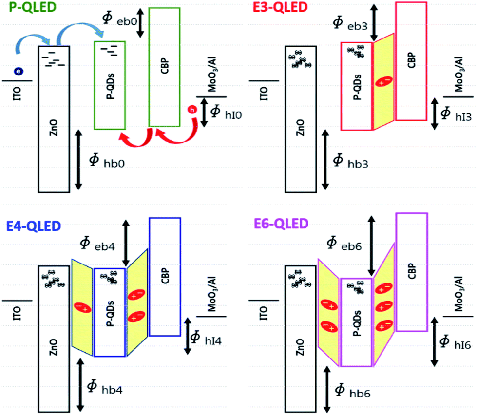 | ||
| Fig. 4 Schematic representation of the energy levels of the QLEDs before and after EDT treatment. The main effects of EDT treatment is the passivation of defect states and formation of surface dipoles that result in vacuum-level shift. Defect-state passivation affect charge-carrier transport and/or recombination, and surface dipole moments alter charge-carrier injection and/or blocking barriers. | ||
4 Conclusions
We have shown that in situ EDT treatment of a QD EML that is formed onto a ZnO-NP ETL by spin-coating colloidal CdSe@ZnS QDs can result in substantial improvement of QLED efficiency. Interestingly, efficiency improvement resulting from in situ EDT treatment showed variable dependence on the concentration of acetonitrile solutions of EDT such that treatment with 3 and 4 mM solutions produced progressive improvement, but treatment at 6 mM resulted in slightly lower efficiency compared to 4 mM treatment. To account for variations in QLED efficiency we separated respective contributions of majority and minority carriers using a phenomenological representation of currents as the sum of two modified Shockley functions that correspond to imperfect diodes. The discrepancy in EDT-concentration and voltage dependence of two current components, which were determined from our phenomenological modeling, was sufficient to elucidate all the main features of luminous–yield curves and their variation with respect to EDT concentrations. Moreover, we deduced systematic variations in response to in situ EDT treatment in an energy-level diagram, which is consistent with respective contributions of majority (electron) and minority (hole) currents for each device. We proposed that dipole moments of EDT molecules induced vacuum-level shifts, and dipole moments were formed at both the EML surface and ETL–EML interface as the result of in situ EDT treatments. Arguably, competition between contributions of dipole moments at the two locations are responsible for variations of electron and hole currents with respect to EDT concentrations. Further studies including separate EDT-treatment of a ZnO ETL and EDT ligand-exchange of colloidal CdSe@ZnS QDs prior to spin-coating are required in order to independently control dipole moments at the EML surface and ETL–EML interface, and to quantify competing contributions of two types of dipole moments.Conflicts of interest
There are no conflicts to declare.Acknowledgements
This work was partly supported by the “Human Resources Program in Energy Technology” from the Korea Institute of Energy Technology Evaluation and Planning (KETEP), grant from the Ministry of Trade, Industry & Energy (MOTIE), Republic of Korea (No. 20164030201380), and partly by the GRRC program of Gyeonggi province [GRRC-AJOU2016B03, Photonics-Medical Convergence Technology Research Center].References
- J. Lim, Y.-S. Park, K. Wu, H. J. Yun and V. I. Klimov, Nano Lett., 2018, 18, 6645–6653 CrossRef CAS PubMed.
- O. Wang, L. Wang, Z. Li, Q. Xu, Q. Lin, H. Wang, Z. Du, H. Shen and L. S. Li, Nanoscale, 2018, 10, 5650–5657 RSC.
- H. Shen, Q. Gao, Y. Zhang, Y. Lin, Q. Lin, Z. Li, L. Chen, Z. Zeng, X. Li, Y. Jia, S. Wang, Z. Du, L. S. Li and Z. Zhang, Nat. Photonics, 2019, 13, 192–197 CrossRef CAS.
- X. Dai, Z. Zhang, Y. Jin, Y. Niu, H. Cao, X. Liang, L. Chen, J. Wang and X. Peng, Nature, 2014, 515, 96–99 CrossRef CAS PubMed.
- T. Cheng, F. Wang, W. Sun, Z. Wang, J. Zhang, B. You, Y. Li, T. Hayat, A. Alsaed and Z. Tan, Adv. Electron. Mater., 2019, 5, 1800794 CrossRef.
- V. K. Sharma, B. Guzelturk, T. Erdem, Y. Kelestemur and H. V. Demir, ACS Appl. Mater. Interfaces, 2014, 6, 3654–3660 CrossRef CAS PubMed.
- S. Pradhan, F. Di Stasio, Y. Bi, S. Gupta, S. Christodoulou, A. Stavrinadis and G. Konstantatos, Nat. Nanotechnol., 2019, 14, 72–79 CrossRef CAS PubMed.
- X. Li, Y. B. Zhao, F. Fan, L. Levina, M. Liu, R. Quintero-Bermudez, X. Gong, L. N. Quan, J. Fan, Z. Yang, S. Hoogland, O. Voznyy, Z. H. Lu and E. H. Sargent, Nat. Photonics, 2018, 12, 159–164 CrossRef CAS.
- P. Vashishtha, M. Ng, S. B. Shivarudraiah and J. E. Halpert, Chem. Mater., 2019, 31, 83–89 CrossRef CAS.
- Y. Yin and A. P. Alivisatos, Nature, 2005, 437, 664–670 CrossRef CAS PubMed.
- T. Zhang, H. Zhao, D. Riabinina, M. Chaker and D. Ma, J. Phys. Chem. C, 2010, 114, 10153–10159 CrossRef CAS.
- C. Ji, M. Lu, H. Wu, X. Zhang, X. Shen, X. Wang, Y. Zhang, Y. Wang and W. W. Yu, ACS Appl. Mater. Interfaces, 2017, 9, 8187–8193 CrossRef CAS PubMed.
- I. Cho, H. Jung, B. G. Jeong, J. H. Chang, Y. Kim, K. Char, D. C. Lee, C. Lee, J. Cho and W. K. Bae, ACS Nano, 2017, 11, 684–692 CrossRef CAS PubMed.
- D. A. R. Barkhouse, A. G. Pattantyus-abraham, L. Levina and H. Edward, ACS Nano, 2008, 2, 2356–2362 CrossRef CAS PubMed.
- X. Jiang, H. Li, Y. Shang, F. Wang, H. Chen, K. Xu, M. Yin, H. Liu, W. Zhou and Z. Ning, Chem. Commun., 2019, 55, 9483–9486 RSC.
- S. Choi, J. Moon, H. Cho, B. H. Kwon, N. S. Cho and H. Lee, J. Mater. Chem. C, 2019, 7, 3429–3435 RSC.
- D. Kim, Y. Fu, J. Kim, K. H. Lee, H. Kim, H. Yang and H. Chae, Nanotechnology, 2016, 27, 245203 CrossRef PubMed.
- H. Zhang, J. Jang, W. Liu and D. V. Talapin, ACS Nano, 2014, 8, 7359–7369 CrossRef CAS PubMed.
- G. Niu, L. Wang, R. Gao, W. Li, X. Guo, H. Dong and Y. Qiu, Phys. Chem. Chem. Phys., 2013, 15, 19595–19600 RSC.
- N. Kirkwood, B. Singh and P. Mulvaney, Adv. Mater. Interfaces, 2016, 3, 1600868 CrossRef.
- B. S. Mashford, M. Stevenson, Z. Popovic, C. Hamilton, Z. Zhou, C. Breen, J. Steckel, V. Bulovic, M. Bawendi, S. Coe-Sullivan and P. T. Kazlas, Nat. Photonics, 2013, 7, 407–412 CrossRef CAS.
- W. K. Bae, J. Kwak, J. W. Park, K. Char, C. Lee and S. Lee, Adv. Mater., 2009, 21, 1690–1694 CrossRef CAS.
- W. K. Bae, K. Char, H. Hur and S. Lee, Chem. Mater., 2008, 20, 531–539 CrossRef CAS.
- Y. J. Lee, C. J. Lee, C. H. Chen, T. C. Lu and H. C. Kuo, IEEE J. Sel. Top. Quantum Electron., 2011, 17, 985–989 CAS.
- P. R. Brown, D. Kim, R. R. Lunt, N. Zhao, M. G. Bawendi, J. C. Grossman and V. Bulović, ACS Nano, 2014, 8, 5863–5872 CrossRef CAS PubMed.
- C. H. M. Chuang, P. R. Brown, V. Bulović and M. G. Bawendi, Nat. Mater., 2014, 13, 796–801 CrossRef CAS PubMed.
- R. Abargues, J. Navarro, P. J. Rodríguez-Cantó, A. Maulu, J. F. Sánchez-Royo and J. P. Martínez-Pastor, Nanoscale, 2019, 11, 1978–1987 RSC.
- A. M. Munro, B. Zacher, A. Graham and N. R. Armstrong, ACS Appl. Mater. Interfaces, 2010, 2, 863–869 CrossRef CAS PubMed.
- N. H. Tuan, S. Y. Ryu, D. A. Tuan and S. Lee, Nanotechnology, 2019, 30, 505202 CrossRef PubMed.
- H. T. Nguyen, N. D. Nguyen and S. Lee, Nanotechnology, 2013, 24, 115201 CrossRef PubMed.
- H. T. Nguyen, H. Jeong, J. Y. Park, Y. H. Ahn and S. Lee, ACS Appl. Mater. Interfaces, 2014, 6, 7286–7291 CrossRef CAS PubMed.
- H. Cho, H. Woo, D. Y. Yoon, K. Char and S. Lee, Nano Lett., 2012, 12, 2362–2366 CrossRef PubMed.
Footnotes |
| † Electronic supplementary information (ESI) available. See DOI: 10.1039/c9ra08411h |
| ‡ These authors contributed equally to this work. |
| This journal is © The Royal Society of Chemistry 2019 |