DOI:
10.1039/C9RA08234D
(Paper)
RSC Adv., 2019,
9, 38047-38054
Improved light-harvesting and suppressed charge recombination by introduction of a nanograss-like SnO2 interlayer for efficient CdS quantum dot sensitized solar cells†
Received
10th October 2019
, Accepted 15th November 2019
First published on 21st November 2019
Abstract
Quantum dot sensitized solar cell (QDSSC) performance is primarily limited by the recombination of charges at the interfaces of TiO2/quantum dot (QD) sensitizer/electrolyte. Hence, blocking or suppressing the charge recombination is an essential requirement to elevate the QDSSC performance to the next level. To retard the charge recombination, herein, we propose the introduction of a SnO2 nanograss (NG) interlayer on the surface of TiO2 using the facile chemical bath deposition method. The SnO2 NG interlayer not only inhibits the interfacial recombination processes in QDSSCs but also enhances the light-harvesting capability in generating more excitons. Hence, the TiO2/SnO2 NG/CdS QDSSCs can achieve the power conversion efficiency of 3.15%, which is superior to that of a TiO2/CdS device (2.16%). Electrochemical impedance spectroscopy, open-circuit voltage decay and dark current analyses confirm that the recombination of charges at the photoanode/electrolyte interface is suppressed and the life time is improved by introducing the SnO2 NG interlayer between the TiO2 and CdS QD sensitizer.
1. Introduction
Because of the increased environmental pollution and the limited fossil fuels, the demand for renewable and sustainable energy systems, such as solar energy, has increased over the last few decades. Among the different solar energy systems, third-generation solar cells such as quantum dot sensitized solar cells (QDSSCs) are gaining considerable interest owing to their advantages of inorganic structure, high theoretical efficiency, easy fabrication and low-cost.1,2 Various metal chalcogenide-semiconductors such as CdS, CdSe, PbS, CdSexS1−x, CuInS2, CuInZnS, etc. have been investigated as promising sensitizers for the QDSSCs due to their tunable band gap, high absorption coefficient and multiple exciton generation (MEG).3–5 A typical structure of the QDSSC is composed of a QD-sensitized TiO2 photoelectrode, polysulfide electrolyte (S2−/Sn2−), and counter electrode, which leads to various hetero-interfaces.6–8 Although QDs have unique characteristics, the QDSSCs achieved a low power conversion efficiency (PCE = 12%) due to the recombination of charges that occur at the photoanode/QDs/electrolyte interfaces.9,10 Hence, considerable attempts have been carried out to suppress the charge recombination, such as the use of a passivation layer on QDs surface, the introduction of metal doping in QDs, and overcoating wide band gap (or insulating) materials over TiO2 surface or QDs, which results in the enhanced QDSSCs performance.11–13
Recently, Z. Ren et al. reported that the application of amorphous TiO2 intermediate layer between the interface of QDs and ZnS/SiO2 layer, effectively suppressed the charge recombination and improved the photovoltaic performance.13 Recently, Li et al. developed the effective integration of ultra-high density well-separated ZnO nanocrystals (NCs) homoepitaxially grown on the surface of an individual vertically oriented single-crystalline (SC) ZnO nanoneedle (NN).14 The fabricated monolithic ZnO NCs-on-NN SC hybrids may hold great promise for enhanced photovoltaic performance (e.g., electron mobility) of ZnO NC-sensitized solar cells. Very recently, Y. S. Lee et al. introduced the TiO2/ZnS/CdS/ZnS cascade structure, in which the presence of ZnS intermediate layers are not only capable of retarding the charge recombination but also improve the light-harvesting efficiency, resulting in the enhanced power conversion efficiency (3.69%).15 Z. Du et al. studied the CdSe QDSSCs based on FTO/TiO2 without and with TiCl4 treatment.16 The QDSSCs based on FTO/TiO2/TiCl4/CdSe photoanode exhibited higher PCE (5.36%) than the FTO/TiO2/CdSe (5.11%), which is mainly due to the TiCl4 treatment that reduced the recombination of charges at the interface of TiO2 and CdSe QDs. Very recently, Ozu et al. reported ZnO nanowire (NW) passivation by an ultrathin SnO2 layer, reducing the density of the deep traps by the absorbed oxygen and hydroxyl groups on the ZnO NW surface.17 SnO2 passivation not only reduced the surface recombination but also led to an upward shift of the Fermi energy, causing more efficient electron transfer to ZnO. Very recently, E. N. Jayaweera et al. developed the SnO2/MgO films for the CdS/ZnS based QDSSCs (SnO2/MgO/CdS/ZnS) to boost the solar cell performance by efficiently preventing the charge recombination at the interface of SnO2/sensitizer.18 As a result, the SnO2/MgO/CdS/ZnS QDSSC achieved a PCE of 1.33%. Therefore, the idea of deposition of wide band-gap semiconductor materials on the surface of semiconductor nanoparticles could effectively improve the QDSSC performance.
Motivated from the recent results of hindering the charge recombination at the TiO2/QDs/electrolyte interfaces, herein, we propose the introduction of a novel SnO2 nanograss (NG) interlayer on TiO2 surface via a simple chemical bath deposition (CBD) route. The deposition of SnO2 NG between the TiO2 and CdS QDs suppresses charge recombination, resulting in enhanced QDSSC performance. Further, the photoanode of TiO2/SnO2 NG/CdS achieves improved light-harvesting and also provides efficient charge transport. The QDSSCs based on TiO2/SnO2 NG/CdS photoelectrode showed an impressive PCE of 3.15% under one sun illumination, which was much higher than that with TiO2/CdS photoelectrode (2.16%). The achieved high efficiency by SnO2 NG interlayer signifies an important approach to further elevate QDSSCs performance to the next level.
2. Experimental section
2.1. Materials
Tin chloride dihydrate (SnCl2·2H2O), hexamethylenetetramine (HMTA, C6H12N4), cadmium acetate dihydrate (Cd(CH3COO)2·2H2O), sodium sulfide (Na2S), sulfur (S) and potassium chloride (KCl) were obtained from Sigma-Aldrich Co., South Korea and used as such without purification. TiO2 paste (Ti-nanoxide HT/SP) was supplied by Solaronix.
2.2. Preparation of TiO2/SnO2 NG/CdS photoelectrode
Prior to the deposition, the fluorine-doped tin oxide (FTO, 13 Ω sq−2) glasses (1.3 × 1.5 cm2) were well washed with acetone, ethanol and deionized (DI) water for 10 min each. Mesoporous TiO2 electrodes were prepared using doctor-blading a TiO2 paste (20 nm diameter, Solaronix SA) onto FTO substrate and then the samples were maintained at 450 °C for 30 min. Then, SnO2 NG was grown on the TiO2 surface via a facile CBD reaction. In detail, 0.05 M SnCl2·2H2O and 0.15 M HMTA were mixed in 70 mL DI water under magnetic stirring for 30 min. The as-prepared TiO2 samples were dipped horizontally into the SnO2 growth solution and heated at 95 °C for 10 h. The HMTA in precursor solution not only serves as a surfactant by reducing the surface tension between the growth solution and substrate, but also it supports the growth of SnO2 layer. After deposition, the SnO2 NG loaded FTO/TiO2 films were rinsed with DI water and ethanol, and then heated at 450 °C for 30 min. The as-fabricated electrodes are termed the TiO2/SnO2 NG.
Next, the CdS QDs were loaded on TiO2/SnO2 NG by a facile successive ionic layer adsorption and reaction (SILAR) method. Briefly, TiO2/SnO2 NG films were dipped in aqueous 0.1 M Cd(CH3COO)2·2H2O solution for 5 min, rinsed with ethanol; then dipped in aqueous 0.1 M Na2S solution for 5 min, and then once again rinsed with ethanol. Such a process is called one SILAR cycle and a totally 8 SILAR cycles were repeated. The as-obtained films are termed the TiO2/SnO2 NG/CdS. The schematic of the fabrication process of TiO2/SnO2 NG/CdS on FTO substrate is shown in Fig. 1.
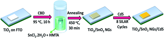 |
| | Fig. 1 The schematic of the preparation process of TiO2/SnO2 NG/CdS on FTO substrate. | |
2.3. Counter electrode and QDSSC device fabrication
CuS counter electrodes were prepared on FTO substrates using CBD method following our previous report.19 Finally, the QDSSCs were sandwiched with as-fabricated TiO2/SnO2 NG/CdS photoelectrodes and CuS counter electrodes by a sealant (SX 1170-60, Solaronix) and polysulfide electrolyte containing of 1 M Na2S, 2 M S and 0.1 M KCl in methanol and water solution (7![[thin space (1/6-em)]](https://www.rsc.org/images/entities/char_2009.gif) :3).
:3).
2.4. Characterization and measurements
The crystalline phase, elemental analysis and morphology of the electrodes were investigated using X-ray diffraction (XRD, D/Max-2400), X-ray photon spectroscopy (XPS, VG Scientific ESCALAB 250) and scanning electron microscope (SEM, S-2400, Hitachi) with energy-dispersive X-ray spectroscopy (EDX, 15 kV) mapping characterizations, respectively. The optical absorption properties of the as-prepared electrodes were analyzed by UV-visible absorption spectra (OPTIZEN 3220UV). The photocurrent–voltage (J–V) measurements were conducted by an ABET Technologies (USA) solar simulator, which can exhibit an intensity of 100 mW cm−2. Electrochemical impedance spectroscopy (EIS) was carried out by a SP-150 BioLogic station with a frequency range of 500 kHz to 0.1 Hz and AC amplitude of 10 mV.
3. Results and discussion
3.1. Structural and morphological characterization
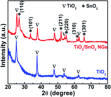
Facile and cost-effective CBD method was used to grow the SnO2 NG interlayer onto the TiO2 surface. Initially, the crystalline structure of the TiO2 and TiO2/SnO2 NG electrodes was investigated using XRD characterization. The XRD patterns of the as-prepared TiO2 and TiO2/SnO2 NG are depicted in Fig. 2. As seen in Fig. 2, both the TiO2 and TiO2/SnO2 NG samples exhibit peaks at 2θ = 25.1°, 37.5°, 47.8°, 53.9° and 62.3°, which are well-matched with the TiO2 tetragonal anatase structure (JCPDS: 21-1272). After the deposition of SnO2 over TiO2 surface, new diffraction peaks are observed at 2θ = 26.7°, 33.6°, 51.9°, 54.9°, 61.5° and 65.8°, which are well-consistent with the SnO2 tetragonal structure (JCPDS: 41-1445).20
 |
| | Fig. 2 XRD patterns of TiO2 and TiO2/SnO2 NG on FTO substrate. | |
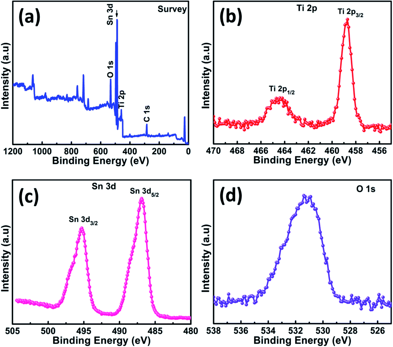
XPS characterization was performed to investigate the valence states of elements in TiO2/SnO2 NG electrode. The XPS survey spectra of TiO2/SnO2 NG sample is shown in Fig. 3a, which clearly shows the presence of only Ti, Sn, O and C elements. The presence of carbon element in the total survey scan spectrum is ascribed to the exposure of air sample to air. As depicted in Fig. 3b, the XPS spectrum of Ti 2p, exhibits the Ti 2p3/2 and Ti 2p1/2 peaks that are centered at 458.7 and 464.5 eV, respectively. These spectra are consistent with the presence of Ti4+ valence state. Due to the spin–orbit coupling of Ti 2p, the obtained peaks are separated by 5.8 eV.21 The Sn 3d spectrum presented in Fig. 3c exhibited two peaks at 486.8 eV and 495.3 eV which are indexed to Sn 3d5/2 and Sn 3d3/2, respectively, and agree with the Sn4+ state in SnO2.22 As depicted in Fig. 3d, the spectrum of O 1s displays a peak that is centered at 530.9 eV, corresponding to O2 in the TiO2 and SnO2 crystal lattices.22,23 The XRD and XPS results confirmed the formation of SnO2 NG on the TiO2 surface.
 |
| | Fig. 3 (a) XPS survey spectra and high-resolution XPS spectra of (b) Ti 2p, (c) Sn 3d and (d) O 1s in TiO2/SnO2 NG sample. | |
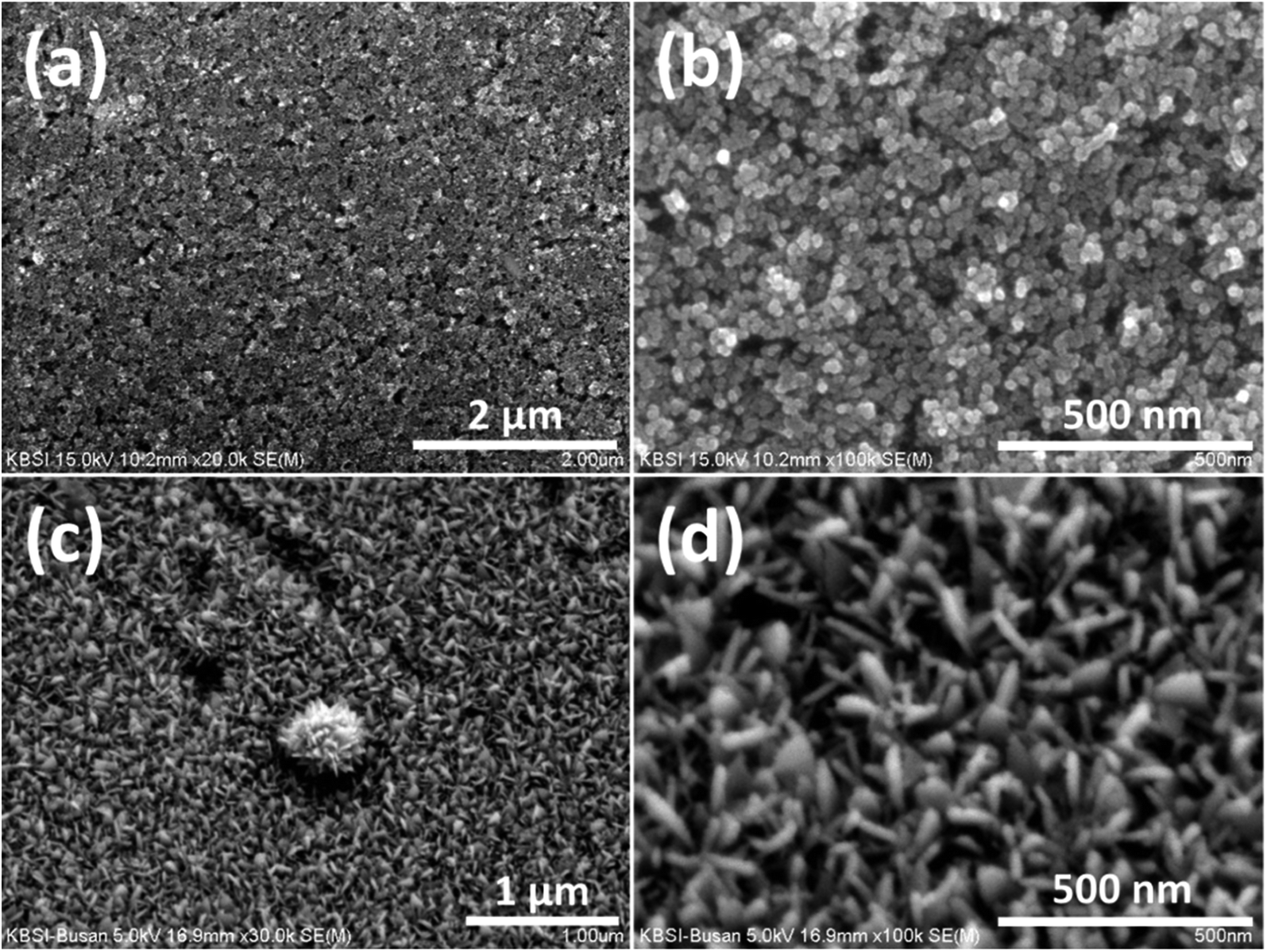
The surface morphologies of the as-prepared TiO2 and TiO2/SnO2 NG electrodes were studied by SEM analysis, and the corresponding images are depicted in Fig. 3a and b for TiO2 on FTO substrate, and in Fig. 4c and d for SnO2 onto the TiO2 surface (TiO2/SnO2) NG. As shown in Fig. 4a, the TiO2 nanoparticles are uniformly distributed throughout the substrate. It can be clearly seen from Fig. 4b, that the TiO2 exhibits spherical nanoparticle morphology with diameter in the range of ∼16 to ∼20 nm. CBD method was used to grow the SnO2 nanostructures on the surface of TiO2. It can be clearly observed in Fig. 4c, that the SnO2 exhibits the nanograss (NG) morphology. The diameter of the SnO2 NG was estimated to be in the range of ∼21 to ∼46 nm (Fig. 4d). The SEM images clearly reveal that the SnO2 NG nanostructures were successfully grown on TiO2 surface. In addition, SEM-EDX color mapping was carried out to examine the distribution of elements in the TiO2/SnO2 NG. The mapping images shown in Fig. S1† clearly revealed the homogeneous distribution of Ti, Sn and O elements in the as-prepared TiO2/SnO2 NG electrode.
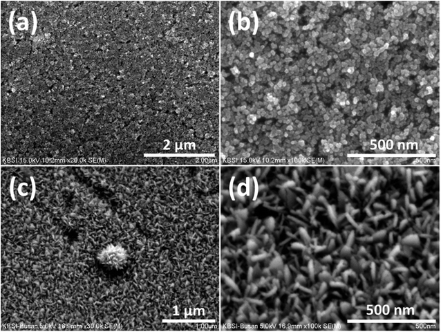 |
| | Fig. 4 SEM images of (a and b) TiO2 and (c and d) TiO2/SnO2 NG on FTO substrate at different magnifications. | |
3.2. Optical properties
UV-vis absorption measurements were carried out to demonstrate the optical properties of the TiO2, TiO2/SnO2 NG, TiO2/CdS and TiO2/SnO2 NG/CdS samples and the results are plotted in Fig. 5 in the rage of 300 to 800 nm. The TiO2 sample exhibits the absorption edge at around 378 nm. The growth of SnO2 NG on TiO2 surface increased the absorption intensity. In addition, the absorption onset of TiO2/SnO2 NG increased to 388 nm. The absorption onsets of the TiO2/CdS and TiO2/SnO2 NG/CdS samples were measured to be 510 nm and 525 nm, respectively. The absorption onset of the TiO2/SnO2 NG/CdS electrode was increased and with higher absorbance compared to TiO2/CdS. These observations can be attributed to the growth of SnO2 NG passivation/barrier layer over TiO2 surface. Also, the SnO2 NG interlayer supports the nucleation and growth of CdS QDs, which results in the high rate absorption of TiO2/SnO2 NG/CdS electrode.
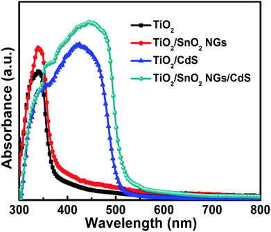 |
| | Fig. 5 UV-vis absorption spectra of as-prepared electrodes. | |
3.3. Photovoltaic performance and charge transfer of the QDSSCs
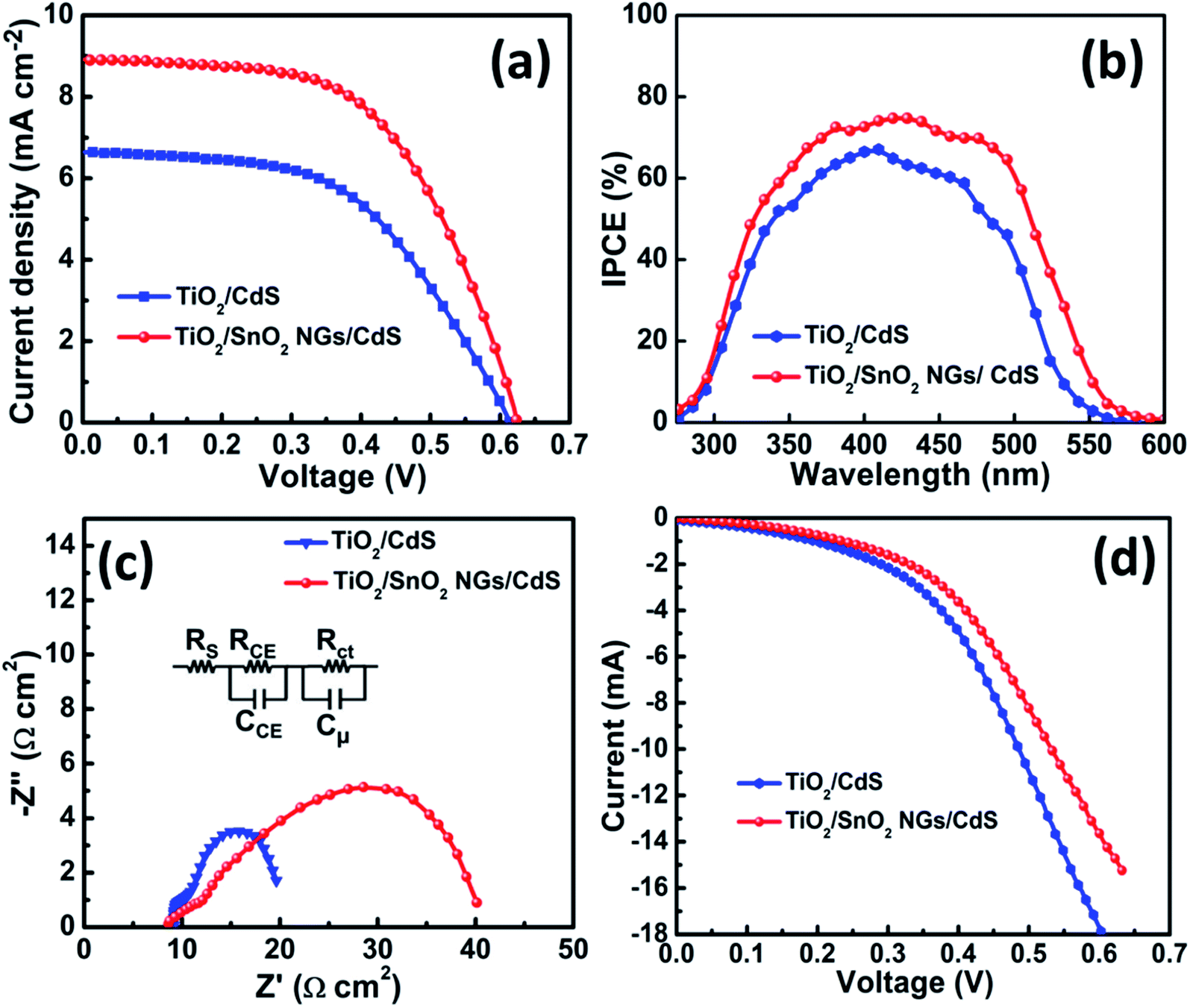
To evaluate the impact of the SnO2 NG interlayer on the photoanodes, the photovoltaic behaviors of TiO2/CdS and TiO2/SnO2 NG/CdS based QDSSCs have been investigated. The J–V profiles of the as-fabricated QDSSCs were measured under one sun illumination and the related photovoltaic considerations are depicted in Fig. 6a and Table 1. The TiO2/CdS QDSSC exhibits JSC of 6.64 mA cm−2, VOC of 0.614 V, and FF of 0.530, resulting in a PCE of 2.16%. When a SnO2 NG layer was grown on TiO2 surface (TiO2/SnO2 NG/CdS), the JSC, VOC and FF were considerably improved to 8.92 mA cm−2, 0.619 V, and 0.570, respectively, resulting in the elevated PCE of 3.15%, which is much higher than the PCE of TiO2/CdS (2.16%) photoelectrode. The enhanced VOC and JSC of the TiO2/SnO2 NG/CdS based QDSSCs are attributed to the reduced charge recombination and the fast charge transfer at the TiO2/QDs/electrolyte interfaces. Hence, the PCE of QDSSC has improved from 2.16% to 3.15% by the growth of SnO2 NG interlayer over the TiO2 surface. Furthermore, incident photon to current conversion efficiency (IPCE) study was carried out to illustrate the light absorption and electron generation behaviors in the QDSSCs. Fig. 6b depicts the IPCE plots of the as-prepared QDSSCs. It is evident from the IPCE spectra that the introduction of SnO2 NG interlayer enhanced the IPCE response from 66% to 75% and also enlarged the IPCE response edge from 548 nm to 568 nm. The TiO2/SnO2 NG/CdS based QDSSCs exhibits higher IPCE response than the TiO2/CdS, which is in good agreement with the JSC of the J–V plots.
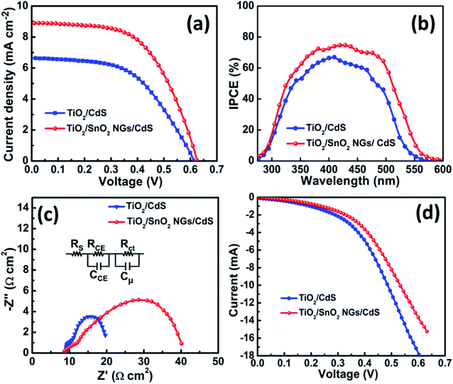 |
| | Fig. 6 (a) J–V, (b) IPCE and (c) EIS profiles of QDSSCs based on TiO2/CdS and TiO2/SnO2 NG/CdS photoelectrodes. (d) J–V profiles of QDSSCs under dark current. | |
Table 1 Photovoltaic parameters of the as-prepared QDSSCs based on TiO2/CdS and TiO2/SnO2 NG/CdS photoelectrodes under one sun illumination
| Cell |
VOC (V) |
JSC (mA cm−2) |
FF |
PCE% |
Rct (Ω) |
Cμ (μm) |
τe (ms) |
| TiO2/CdS |
0.614 |
6.64 |
0.530 |
2.16 |
8.78 |
1358 |
11.92 |
| TiO2/SnO2 NG/CdS |
0.619 |
8.92 |
0.570 |
3.15 |
27.94 |
2183 |
60.99 |
In order to demonstrate the impact of SnO2 NG interlayer on the photoelectrode films, EIS measurement was conducted under forward bias (VOC) and illumination. The Nyquist plots of the TiO2/CdS and TiO2/SnO2 NG/CdS based QDSSCs are depicted in Fig. 6c. The Nyquist plots of both devices exhibit the two semicircles, in which the first (small) semicircle is obtained in the high-frequency region and represents the charge transfer resistance (RCE), the chemical capacitance (CCE) at the interface of the counter electrode/electrolyte, and the series resistance (RS) which is obtained in the high-frequency region where the phase is zero. The recombination resistance (Rct) at the TiO2/QD/electrolyte interface and the chemical capacitance (Cμ) indexed to the bigger semicircle which is obtained at mid/low frequency.24,25 Based on the equivalent circuit model (inset of Fig. 6c) and using Z-view software, the Nyquist plots were fitted to obtain the Rct values and the fitting results are summarized in Table 1. There is no considerable change in the RCE, which is due to the usage of similar electrolyte and counter electrode in the fabrication of QDSSCs. However, Rct of the TiO2/SnO2 NG/CdS based QDSSC (27.94 Ω cm2) is much higher than that of the TiO2/CdS (8.78 Ω cm2). The higher Rct of the TiO2/SnO2 NG/CdS based QDSSC demonstrates that the growth of SnO2 NG over the TiO2 surface successfully suppresses the electron recombination at the TiO2/QDs/electrolyte interfaces.24 Hence, the growth of SnO2 NG interlayer hinders the interfacial charge recombination and enhances the photovoltaic performance (JSC and FF). Moreover, QDSSC based on TiO2/SnO2 NG/CdS photoelectrode achieves higher Cμ (2183 μF) than that of the TiO2/CdS (1358 μF) system. The higher Cμ of the TiO2/SnO2 NG/CdS system demonstrates the improved collection of photo-excited electrons into the conduction band of photoanode, which is mainly due to the hindered recombination at the TiO2/QDs/electrolyte interfaces. Further, the electron life time (τe) of the QDSSCs can be obtained using the following equation,26
Interestingly, the
τe of the TiO
2/CdS with SnO
2 NG interlayer (60.99 ms) is much higher than that of the SnO
2 NG-free device (11.92 ms), which reveals the higher charge collection efficiency of the TiO
2/SnO
2 NG/CdS system.
Under the dark condition, the J–V plots of the TiO2/CdS and TiO2/SnO2 NG/CdS based QDSSCs were obtained and are shown in Fig. 6d. The electron recombination occurs at the interfaces of TiO2/QDs and TiO2/electrolyte, and this is the source of dark current.27 Hence, a dark current study is a useful indicator of charge recombination. With the introduction of SnO2 NG interlayer, the TiO2/SnO2 NG/CdS device delivers the reduced dark current, which is lower compared with that of the TiO2/CdS device. The reduction of the dark current arose from an enhancement in electron transport with decreasing the internal resistance. As a result, the electron recombination was effectively reduced by the introduction of the SnO2 NG interlayer, and this contributed to the enhanced current and decreased electron loss.
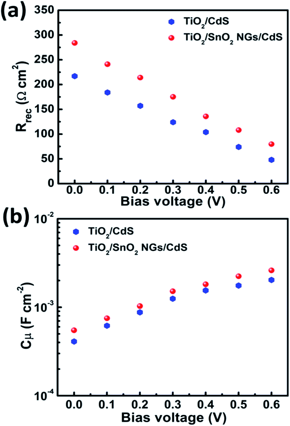
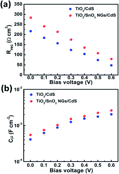
Furthermore, to investigate the impact of SnO2 NG interlayer on the performance of QDSSCs, EIS tests were conducted at various bias applied voltages under dark condition in the 500 kHz to 100 mHz frequency range. The obtained recombination resistance (Rrec) and chemical capacitance (Cμ) from the corresponding EIS tests are depicted in Fig. 7a and b, respectively. The Rrec and Cμ reveal that the charge recombination process occurs at the TiO2/QDs/electrolyte interfaces. A higher Rrec represents the low recombination rate and grater Cμ values denote the Fermi level upward shift, yielding the enhanced VOC.16 It can be seen from Fig. 6a that the Rrec values of both devices decrease with the increment of the forward bias voltage due to the increased Fermi level of TiO2 at the forward bias. Also, TiO2/SnO2 NG/CdS QDSSCs exhibits higher Rrec values than the TiO2/CdS device under identical bias voltages. The recombination rate is inversely proportional Rrec.13 Moreover, the higher Cμ values of the TiO2/SnO2 NG/CdS device denote the upward shift of the Fermi level of TiO2, resulting in large VOC. These EIS studies reveal the reduced recombination rate for the TiO2/SnO2 NG/CdS device, which is favorable for the improved JSC and FF.
 |
| | Fig. 7 EIS (a) recombination resistance (Rrec) and (b) chemical capacitance (Cμ) at various forward bias voltages (V). | |
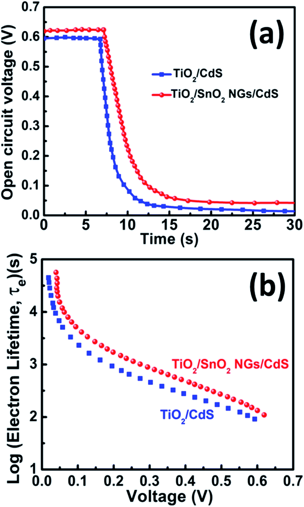
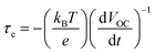
The excited electrons life time was examined using the open-circuit voltage (VOC) decay studies with time. Initially, the QDSSCs were irradiated with one sun illumination to a steady voltage, then the illumination was turned off and the VOC decay data was obtained. Fig. 8a depicts the VOC decay profiles of the TiO2/CdS and TiO2/SnO2 NG/CdS based QDSSCs. The VOC decay plots clearly exhibit the continued monitoring of VOC values under illumination and approach to decay after switching off the illumination. It is evident from the VOC decay plots that the TiO2/SnO2 NG/CdS based QDSSCs exhibit a slower voltage decay rate than the TiO2/CdS photoanode. This behavior is mainly attributed to the SnO2 NG interlayer which efficiently suppresses the charge recombination at the TiO2/QDs/electrolyte interfaces and also promotes the efficient electron transfer. Further, the electron life time (τe) can be estimated using the following equation:28
| |
 | (2) |
where,
kB,
T and
e have their usual meanings.
Fig. 8b displays the plot of electron life time (
τe, in log sign) as a function of
VOC.
29 The TiO
2/SnO
2 NG/CdS based QDSSCs deliver longer
τe values than that of TiO
2/CdS, implying a suppressed recombination of the photo-generated electrons leading to the efficient charge transfer, which agrees well with the EIS analysis.
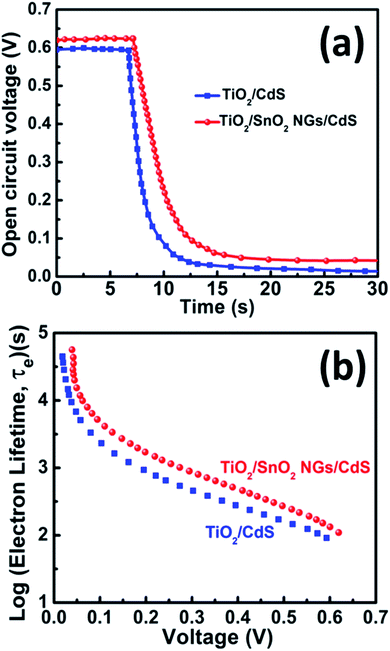 |
| | Fig. 8 (a) VOC decay profiles of TiO2/CdS and TiO2/SnO2 NG/CdS QDSSCs. (b) Electron life time (in log-linear notation) obtained from VOC decay measurements. | |
Fig. 9 depicts the impact of the SnO2 NG interlayer on the charge transfer mechanism in QDSSCs. As shown in Fig. 9a, upon illumination, CdS captures the photons and produces the electron–hole pairs, named excitons. Then the electrons transfer into TiO2 conduction band, while the holes are reduced by polysulfide electrolyte. Simultaneously, the possibility of charge recombination also takes place at the interfaces of TiO2/CdS QDs/electrolyte, which results in poor photovoltaic performance (Fig. 9a). Hence, SnO2 NG interlayer was introduced between the TiO2 and CdS QDs (TiO2/SnO2 NG/CdS) to prevent the charge recombination (Fig. 9b). The introduction of SnO2 NG interlayer on TiO2 surface retards the back injection of the electron from TiO2 to QDs and also prevents the injection of excited electron from TiO2 to redox couple, resulting in the high photovoltaic performance. Therefore, introducing SnO2 NG interlayer over the TiO2 surface achieves the outstanding properties, such as wide solar light-harvesting ability, enhanced charge transfer and suppressed charge recombination at the TiO2/QDs/electrolyte interfaces.
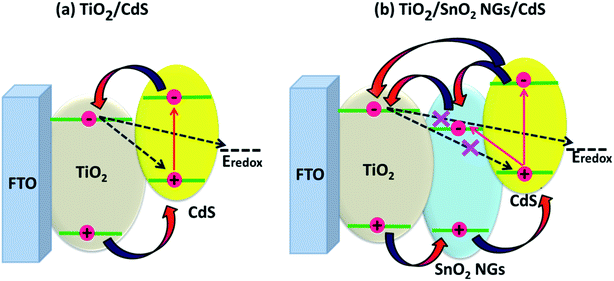 |
| | Fig. 9 Schematic demonstration of the charge transfer pathways in (a) TiO2/CdS and (b) TiO2/SnO2 NG/CdS based QDSSCs. | |
4. Conclusions
In summary, the introduction of SnO2 NG layer between the TiO2 and CdS QDs achieved the higher light-harvesting ability, improved charge transport and suppressed charge recombination at the TiO2/QDs/electrolyte interfaces. Evident from the J–V, EIS, IPCE, VOC decay and dark current measurements indicate that the photovoltaic properties of the TiO2/CdS QDSSCs were drastically enhanced after the deposition of SnO2 NG layer due to the improved light absorption, fast charge transfer, reduced charge recombination and prolonged electron life time. Hence, the introduction of SnO2 NG interlayer could be a favorable and effective approach to considerably improve the performance of QDSSCs. As a result, TiO2/SnO2 NG/CdS based QDSSCs achieved the PCE (3.15%), VOC (0.619 V), JSC (8.92 mA cm−2), and FF (0.570), respectively, which are superior to TiO2/CdS device (PCE = 2.16%, VOC = 0.614 V, JSC = 6.64 mA cm−2, and FF = 0.530).
Conflicts of interest
The authors declare no competing financial interest.
Acknowledgements
This work was supported by UAEU Program for Advanced Research (UPAR) under grant no. 31S312. Also, this work was supported by BK 21 PLUS, Creative Human Resource Development Program for IT Convergence, Pusan National University, Busan, South Korea.
References
- W. Li and X. Zhong, J. Phys. Chem. Lett., 2015, 6, 796–806 CrossRef CAS PubMed.
- A. J. Nozik, M. C. Beard, J. M. Luther, M. Law, R. J. Ellingson and J. C. Johnson, Chem. Rev., 2010, 110, 6873–6890 CrossRef CAS PubMed.
- M. Ye, X. Gao, X. Hong, Q. Liu, C. He, X. Liu and C. Lin, Sustainable Energy Fuels, 2017, 1, 1217–1231 RSC.
- Z. Y. Yang, J. Z. Fan, A. H. Proppe, F. P. Arquer, D. Rossouw, O. Voznyy, X. Z. Lan, M. Liu, G. Walters, R. Q. Bermudez, B. Sun, S. Hoogland, G. A. Botton, S. O. Kelley and E. H. Sargent, Nat. Commun., 2017, 8, 1325 CrossRef PubMed.
- R. L. Wu, T. Y. Wang, M. Wu, Y. B. Lv, X. P. Liu, J. J. Li, H. B. Shen and L. S. Li, Chem. Eng. J., 2018, 348, 447–454 CrossRef CAS.
- H. J. Kim, S. W. Kim, C. V. V. M. Gopi, S. K. Kim, S. S. Rao and M. S. Jeong, J. Power Sources, 2014, 268, 163–170 CrossRef CAS.
- M. P. A. Muthalif, C. D. Sunesh and Y. Choe, Appl. Surf. Sci., 2018, 440, 1022–1026 CrossRef.
- P. Subramanyam, P. Ghosal, M. Deepa and C. Subrahmanyam, Electrochim. Acta, 2018, 278, 374–384 CrossRef CAS.
- W. Wang, W. L. Feng, J. Du, W. N. Xue, L. L. Zhang, L. L. Zhao, Y. Li and X. H. Zhong, Adv. Mater., 2018, 30, 1705746 CrossRef PubMed.
- C. V. V. M. Gopi, M. V. Haritha, S. K. Kim and H. J. Kim, Nanoscale, 2015, 7, 12552–12563 RSC.
- F. Huang, Q. Zhang, B. Xu, J. Hou, Y. Wang, R. C. Masse, S. Peng, J. Liu and G. Cao, J. Mater. Chem., 2016, 4, 14773–14780 RSC.
- C. V. V. M. Gopi, M. V. Haritha, H. Seo, S. Singh, S. K. Kim, M. Shiratani and H. J. Kim, Dalton Trans., 2016, 45, 8447–8457 RSC.
- Z. Ren, J. Wang, Z. Pan, K. Zhao, H. Zhang, Y. Li, Y. Zhao, I. M. Sero, J. Bisquert and X. Zhong, Chem. Mater., 2015, 27, 8398–8405 CrossRef CAS.
- J. M. Li, CrystEngComm, 2017, 19, 32–39 RSC.
- Y. S. Lee, C. V. V. M. Gopi, M. V. Haritha and H. J. Kim, Dalton Trans., 2016, 45, 12914–12923 RSC.
- Z. Du, H. Zhang, H. Bao and X. Zhong, J. Mater. Chem. A, 2014, 2, 13033–13040 RSC.
- S. Ozu, Y. Zhang, H. Yasuda, Y. Kitabatake, T. Toyoda, M. Hirata, K. Yoshino, K. Katayama, S. Hayase and R. Wang, Front. Energy Res., 2019, 7, 11 CrossRef.
- E. N. Jayaweera, G. R. A. Kumara, C. Kumarage, S. K. Ranasinghe, R. M. G. Rajapakse, H. M. N. Bandara, O. A. Ileperuma and B. S. Dassanayake, J. Photochem. Photobiol., A, 2018, 364, 109–115 CrossRef CAS.
- C. V. V. M. Gopi, M. V. Haritha, S. K. Kim, S. S. Rao, D. Punnoose and H. J. Kim, RSC Adv., 2015, 5, 2963–2967 RSC.
- G. E. Patil, D. D. Kajale, V. B. Gaikwad and G. H. Jain, Int. Nano Lett., 2012, 2, 1–5 CrossRef.
- A. Ray, A. Roy, P. Sadhukhan, S. R. Chowdhury, P. Maji, S. K. Bhattachrya and S. Das, Appl. Surf. Sci., 2018, 443, 581–591 CrossRef CAS.
- D. Wang, M. Zhang, Z. Chen, H. Li, A. Chen, X. Wang and J. Yang, Sens. Actuators, B, 2017, 250, 533–542 CrossRef CAS.
- A. Hodaei, A. S. Dezfuli and H. R. Naderi, J. Mater. Sci.: Mater. Electron., 2018, 29, 14596–14604 CrossRef CAS.
- F. Huang, J. Hou, Q. Zhang, Y. Wang, R. C. Massé, S. L. Peng, H. L. Wang, J. S. Liu and G. Z. Cao, Nano Energy, 2016, 26, 114–122 CrossRef CAS.
- R. Zhou, Q. F. Zhang, E. Uchaker, J. Lan, M. Yin and G. Z. Cao, J. Mater. Chem. A, 2014, 2, 2517–2525 RSC.
- H. Kim, G. Xu, C. V. V. M. Gopi, H. Seo, M. V. Haritha and M. Shiratani, J. Electroanal. Chem., 2017, 788, 131–136 CrossRef CAS.
- J. Bisquert, A. Zaban, M. Greenshtein and I. M. Seró, J. Am. Chem. Soc., 2004, 126, 13550–13559 CrossRef CAS PubMed.
- S. B. Ambade, R. B. Ambade, R. S. Mane, G. W. Lee, S. F. Shaikh, S. A. Patil, O. S. Joo, S. H. Han and S. H. Lee, Chem. Commun., 2013, 49, 2921–2923 RSC.
- H. Seo, D. Ichida, S. Hashimoto, N. Itagaki, K. Koga, M. Shiratani, S. H. Nam and J. H. Boo, J. Nanosci. Nanotechnol., 2016, 16, 4875–4879 CrossRef CAS PubMed.
Footnote |
| † Electronic supplementary information (ESI) available. See DOI: 10.1039/c9ra08234d |
|
| This journal is © The Royal Society of Chemistry 2019 |
Click here to see how this site uses Cookies. View our privacy policy here. 
 Open Access Article
 This Open Access Article is licensed under a Creative Commons Attribution-Non Commercial 3.0 Unported Licence
 *b,
Hee-Je Kim
*b,
Hee-Je Kim