
 Open Access Article
 This Open Access Article is licensed under a Creative Commons Attribution-Non Commercial 3.0 Unported Licence
Thermo and flex multi-functional array ionic sensor for a human adaptive device†
Sukjin Jangab,
Daehwan Choiab,
Suk Yangab and
Jang-Yeon Kwon *ab
*ab
aSchool of Integrated Technology, Yonsei University, Incheon 21983, Republic of Korea. E-mail: jangyeon@yonsei.ac.kr
bYonsei Institute of Convergence Technology, Yonsei University, Incheon 21983, Republic of Korea
First published on 13th November 2019
Abstract
Recently, electronic skin that mimics human skin in measuring tactile stimuli, temperature, and humidity and having a self-healing function was developed. Furthermore, with the advances in the field of artificial intelligence and health monitoring, various materials and methods have been studied for e-skin. The limitations to work on actual human skin include device flexibility and large-area applications through array structures, and many studies are underway to overcome these problems. Polymeric materials containing ionic liquids can be used to easily fabricate devices in the solid state. They are highly sensitive to both pressure and temperature, making them suitable for multi-sensing devices. Resistive and capacitive sensors have the advantage of having a simple structure, which makes them easy to fabricate. In a single device, both types work well. For resistive sensors, the temperature sensitivity (1.1/°C) is relatively high. Conversely, capacitive sensors have a low temperature sensitivity (0.3/°C). However, they have the advantage of being uniformly variable under each condition and having a smaller error range. In the array structure, independent flex and thermo sensors are arranged repeatedly. The resistive type shows changes in temperature and bending, but in the capacitive type, it is difficult to obtain results from the pixels due to parasitic capacitance.
1. Introduction
Electronic skin (e-skin), which mimics human skin and is capable of performing its functions, has been studied in various applications such as wearable,1–4 self-healing,5,6 and multi-functional sensing devices7–12 and robotics.13,14 With regard to mimicking the functions of human skin, an artificial skin can detect multiple physical and chemical stimuli such as temperature and humidity. Recently, the use of artificial skin has also been expanded to robotics, and it has been used in artificial intelligence based self-learning prosthetics.15 This requires surfaces with a wide sensing space and simple structure as well as simultaneous sensing through arraying, and devices that can measure different kinds of stimuli will be the focus of next-generation e-skin studies.Ionic materials, such as real organic materials, consist of cations and anions, and are suitable for biomimetic devices. However, there have been few studies on the expansion into large-area array structures using these ionic materials. In addition, due to the nature of e-skin exposure to the external environment, there are difficulties in accurately measuring ionic substances that are sensitive to various conditions.16 There have also been many reports of sensitive changes in both capacitance and resistivity in various environments.17–23 The mechanisms and characteristics of the two parameters are significantly different; therefore, it is important to have a transduction method for taking measurements of e-skin.
In order to mimic the tactile sensing of the human skin, it is essential to use arrays, and in terms of price and reproducibility, it is advantageous to use sensors with many arrays that simplify the structure of each pixel. In this study, an ionic thermoplastic polyethylene (i-TPU) with a certain area is used as a single pixel device. As a material satisfying these conditions, many previous reports have shown that i-TPU is highly suitable for developing sensors that mimic the human body.24–26 The role of the ionic liquid is defined by two things: one is the human adaptive device, which actually mimics the human body composed of various electrolytes and ions. Another is that because of the ionic liquid, the cations and anions move between the segments of the polymer, resulting in higher conductivity and capacitance values compared to conventional polymeric materials. It has the electrical properties of ionic materials as well as the elastomer properties of thermoplastic polyurethane (TPU); hence, it is not only stretchable but also easy to be formed into the desired structure. In other words, the i-TPU itself can be used to form the structure of the sensing device. It is also known that the electrical properties of ionic substances vary with temperature.27,28
In this study, two types of i-TPU films with different heights are repeatedly arranged. It is measured in terms of the current and capacitance by using a simple structure in which electrodes are connected only at the top and bottom. For i-TPUs with relatively greater heights, there will be no change in the electrical characteristics in response to external bending; however, it is sensitive to changes in temperature. In contrast, the lower one is used as a bending sensor rather than as an ambient temperature sensor. Finally, we produced a 6 × 6 array and measured and mapped each current and capacitance value to see the changes in the element due to temperature and bending. In this way, resistance and capacitance type sensors are directly compared, and the differences of each device and array structure are studied. Based on this, we developed a multi-functional array sensor that can measure temperature and bending at the same time.
2. Experiment
2.1 Synthesis of i-TPU
Thermoplastic polyurethane (TPU) beads were purchased from KOLON INDUSTRIES, INC. The N,N-dimethylformamide (DMF) used for the TPU beads solvent was purchased from Sigma-Aldrich. The 1-ethyl-3-methylimidazolium bis(trifluoromethylsulfonyl)imide [EMIM]+[TFSI]− was provided by C-TRI INDUSTRIE, INC. First, the TPU beads were dissolved in DMF at a weight ratio of 1![[thin space (1/6-em)]](https://www.rsc.org/images/entities/char_2009.gif) :5, and the solution was stirred at 130 °C for 2 h. After all the TPU beads were dissolved into the DMF, 20 wt% ionic liquid, [EMIM]+[TFSI]− (depending on the weight of the TPU beads) was added to the solution followed by additional stirring at 130 °C for 1 h. This blended i-TPU solutions are used in two ways. The first is evaporation DMF to form an i-TPU film and the other is used as an ionic glue in a liquid state. The i-TPU film was cured in a box furnace at 130 °C for 12 h to solidify it like polymer. The thickness of the film was controlled according to the weight of the liquid. Then, we cut it into a square of 3 mm × 3 mm, which is the size of the pixel.
:5, and the solution was stirred at 130 °C for 2 h. After all the TPU beads were dissolved into the DMF, 20 wt% ionic liquid, [EMIM]+[TFSI]− (depending on the weight of the TPU beads) was added to the solution followed by additional stirring at 130 °C for 1 h. This blended i-TPU solutions are used in two ways. The first is evaporation DMF to form an i-TPU film and the other is used as an ionic glue in a liquid state. The i-TPU film was cured in a box furnace at 130 °C for 12 h to solidify it like polymer. The thickness of the film was controlled according to the weight of the liquid. Then, we cut it into a square of 3 mm × 3 mm, which is the size of the pixel.
2.2 Fabrication of single and 6 × 6 array sensors
The top and bottom polyimide (PI, Vtec PI-1388 Plastic Resin) films were formed on a silicon substrate by spin coating. For the patterning process, we used the AZ 5214E photoresist (PR) and a maskless lithography tool (Nano System Solutions, Inc.). The PR was spin-coated at 4000 rpm for 30 s and baked at 110 °C for 50 s. The electrode pattern was exposed to 30 mJ with an h-line (405 nm) light source, and then the sample was baked at 120 °C for 2 min, followed by UV irradiation under 200 mJ. After development, the PR in the unexposed area was removed. A 50 nm-thick Mo film was deposited by direct current (DC) sputter. The residue of PR on the substrate was dissolved by ultrasonication in acetone. After that, we pasted i-TPU mechanotransducer pixel (IMP) on the bottom substrate using ionic glue.2.3 Measurement method
The multi-sensing array was measured in an ambient environment at room temperature. Current characterization was performed using a Kiethley 4200-SCS parameter analyzer. All the results were measured under 5 V. The capacitive properties of the i-TPU were measured using a two-probe method (Impedance analyzer E4990 A, Keysight Technologies) at DC: 0 V, AC: 500 mV and frequency: 100 Hz.3. Results and discussion
In this experiment, we present a method for measuring temperature and flexion simultaneously using a single ionic material. Here, i-TPU operates as a high-sensitivity thermo sensor due to the high temperature coefficient of the material. Fig. 1a represents the molecular components of the i-TPU dielectric, which is prepared from the non-covalent association [EMIM]+[TFSI]− cation–anion pairs loaded in the TPU. chemical structure of i-TPU. To provide a more detailed description of the structure, the schematic of the side view is shown in Fig. 1b. The pixel used for temperature measurement, which is called ionic thermotransducer pixel (ITP), has a relatively greater height (H1) and is in contact with both the top and bottom electrodes, thereby forming a typical metal-insulator-metal structure. It does not respond to the degree of external bending, but it is very sensitive to the temperature at the surface. Two ITPs of the same height are used as pillars for a single device, and the ionic mechanotransducer pixel (IMP), which has a relatively lower height (H2), is placed in between and is not in contact with the top electrode. However, when banding is applied, the PI on the outer wall becomes bent or crumpled and comes into contact with the top electrode. The size of each i-TPU pixel is 3 mm × 3 mm, and the distance between each pixel is 2 mm. We can control the height of the i-TPU; H1 is 550 μm (error range: 20 μm). The height ratio with the flexion sensor pixel is denoted as h, where h = H2/H1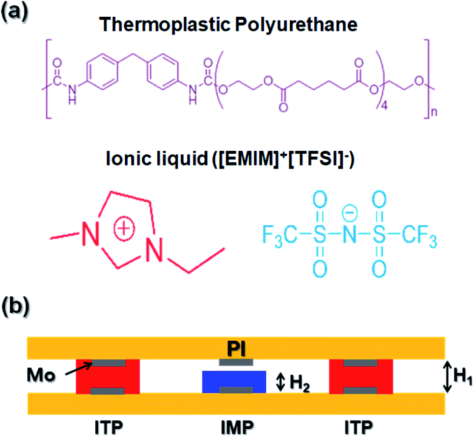 | ||
| Fig. 1 (a) Chemical structure of the thermoplastic polyurethane and the [EMIM]+[TFSI]− ionic liquid (b) schematic of side view image of thermo flex multi-functional array sensor having i-TPU pixels on the PI substrate. | ||
Fig. 2a shows the change in current with a single i-TPU depending on the temperature. The temperature was measured from room temperature up to 40 °C within the range of human body temperature. The structure in which gold film was deposited over the i-TPU, which was placed over the copper electrode, was measured as shown in the figure. It can be seen that the value of current increased from 1 μA to 18 μA when the temperature was increased from 22 °C to 37 °C.
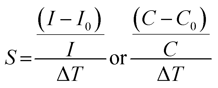
The blue diamond-shaped graph represents the value of relative change and is an indicator of the amount of increase compared to the initial value. This is represented by the formula (I − I0)/I0. In this case, the initial current I0 is the current at 22 °C and will change depending on the experimental environment and conditions. Therefore, in this study, we will introduce the concept of temperature sensitivity, which is a distribution of this value in terms of temperature according to the follow equation.
where E is the activation energy for ionic construction, σ0 is a material constant, and k is the Boltzmann constant. The ESI Fig. 1† shows log
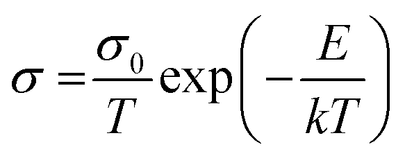 σ vs. 1/T plot that has linear relationship, it can be seen that voltages above 5 V are in accordance with the conventional Arrhenius equation.
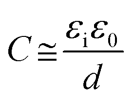
Fig. 2b shows the measurement of the capacitance value of the same device whose current was measured. The measurements were taken from 22 °C to 39 °C and a sensitivity of approximately 0.3/°C was obtained. The increase in temperature causes an electric double layer (EDL), which leads to an increase in capacitance with temperature. The ESI Fig. 2† shows EDL raw data of Fig. 2b that has EDL properties in EDL capacitor. The capacitance in EDL model is defined as
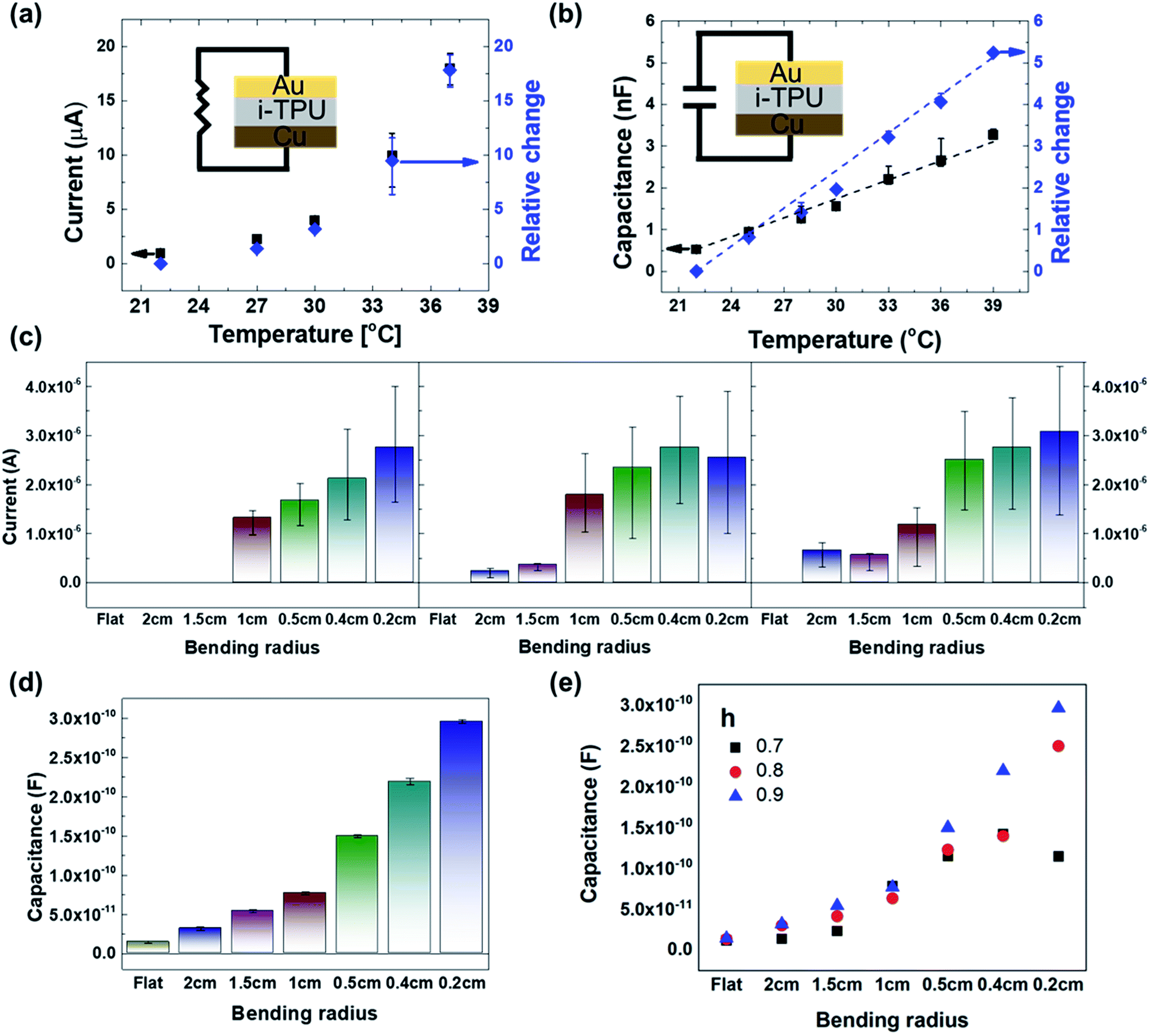 | ||
| Fig. 2 (a) Current and relative change of single i-TPU device as a function of temperature. (b) Capacitance and relative change of single i-TPU device as a function of temperature. (c) Current in terms of bending radius under 3 conditions of h (which is the height ratio). (d) Capacitance in terms of bending radius when h is 0.9. (e) Summary of average capacitance when h is 0.7, 0.8, and 0.9. | ||
In the case of a single device, the resistance type sensor has high sensitivity. However, the capacitance type sensor has a small error range, and linear characteristics, it is advantageous to calculate the specific value within the range when taking measurements.
Fig. 2c shows the currents in single flex sensors under various bending radii. We fabricated a substrate using Teflon with each bending radius and measured the device under flexion (see ESI Fig. 3†). The values of the height ratio h were 0.5, 0.7, and 0.9. As the bending radius decreases, it bends at a larger angle, and the stress on the device increases. First, when h is 0.5, the difference between the heights of IMP and ITP is doubled, and there is no current flow at 2 and 1.5 cm, which means that the i-TPU could not come into contact with the top electrode. If the height of the IMP is increased to 0.7 or higher, the current flows even at 2 cm, which is a relatively gentle curve.
There are two exceptions to the experimental results: the current value at 0.4 cm is greater than 0.2 cm (h = 0.7) and the current value at 2 cm is greater than 1.5 cm (h = 0.9). In some cases, there are not many samples, but it may be said that the strain received by the actual device is relatively small. In addition, in the case of flexion test, it is confirmed that the error is larger than the range of the temperature sensor. Earlier, it was seen that a capacitance type sensor array is not suitable for temperature sensing; a single device was found to have a very narrow error range. We also checked if the same result was obtained in flexion sensing.
Fig. 2d shows the value of capacitance with various bending radii in the same device. Due to the parasitic capacitance, it is also measured in a flat state, and it shows a tendency for the capacitance to increase at high values of strain. The error range is negligible, indicating that it is a better sensor when used a single device. Fig. 2e shows the tendency of the capacitance type IMP for three different heights. The highest capacitance was obtained when h = 0.9, but the difference is negligible in all the three cases, and the same trend is seen at lower flexion stress. This is similar to the previously reported result for the pressure sensor with flat i-TPU film.
So far, we examined the performances of temperature and flexion sensors when i-TPU is a single device. Based on the above results, the array structure shown in Fig. 3a is designed to see how it works in an array structure.
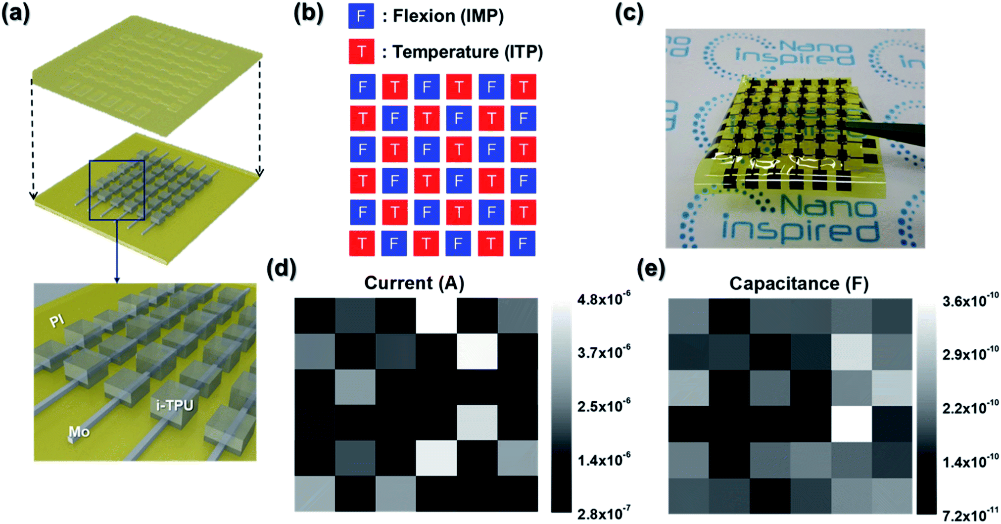 | ||
| Fig. 3 (a) Schematic of array with PI sandwich structure. (b) Mapping the position of each pixel. (c) Optical image of the actual fabricated flexible device. (d) Initial mapping data of a resistive type array sensor. (e) Initial mapping data of a capacitance type array sensor. | ||
The basic structure is the same as that in Fig. 1b, with the IMPs surrounded by ITPs. By repeatedly positioning the two sensors, we tried to obtain the temperature and bending information of each location. This structure was constructed by repeatedly arranging the devices in a 6 × 6 array (consisting of 36 pixels) as shown in Fig. 3b, and the array consisted of IMPs (pixels of flexion sensor), and ITPs (pixels of temperature sensor). Through the idea of a simple structure with one material but different heights, we wanted to obtain information about the changes in one or more stimuli. Fig. 3c shows an optical image of a flexible device, which is a thermo flex multi-functional sensor.
Fig. 3d shows the initial state of the device mapping the measured current when h is 0.9. The color of the pixel turns from black to white to indicate an increase in current. The composition of each pixel is shown in Fig. 3b. For the resistance type sensor, there are variations depending on the pixels, and it can be found that the value of current is generally low for the IMP and high for the ITP. From the actually measured values, it is seen that the average value of 18 pixels of ITP is 2.6 μA and that of IMP is 0.76 μA, which is a difference of about 3 times.
The mapping data of the capacitance measured with the same device is shown in Fig. 3e. In capacitance measurement, IMP and ITP are relatively indistinguishable unlike that in current measurement. From the actually measured values, the average value of 18 pixels of ITP is found to be 1.9 nF while that of IMP is 1.8 nF, which are almost the same. When the ionic material encounters the electrode, the cations and anions move to the surface, forming an EDL. The organically connected electrodes, which are not in direct contact, prevent the pixels from operating independently and are affected by the different capacitances. The capacitance type sensor is not suitable for this array structure. After that, array devices with these initial characteristics were measured at various temperatures and bending radii.
Fig. 4a shows the current mapping results as a function of temperature. The currents of all 36 pixels were measured by increasing the temperature. At this time, it has h = 0.9 and is measured on a silicon substrate to create a completely flat state. In a device in a perfectly flat state, the IMP does not have any current flow because the top electrodes are not connected. Naturally, it can be seen that the value does not change even when the temperature increases. For ITP, there is a deviation from pixel to pixel, but it appears to become brighter when the temperature increases from 28 to 40 °C. Although it is possible to check the distribution of approximate values by mapping, it is difficult to know the exact amount of variation in the array structure. Therefore, the relative change in the 18 current values of the ITP was calculated for each temperature (Fig. 4b). With 28 °C as the initial value, the sensitivity between 28 and 40 °C is approximately 0.04/°C, which is about 27 times less than that of a single device.
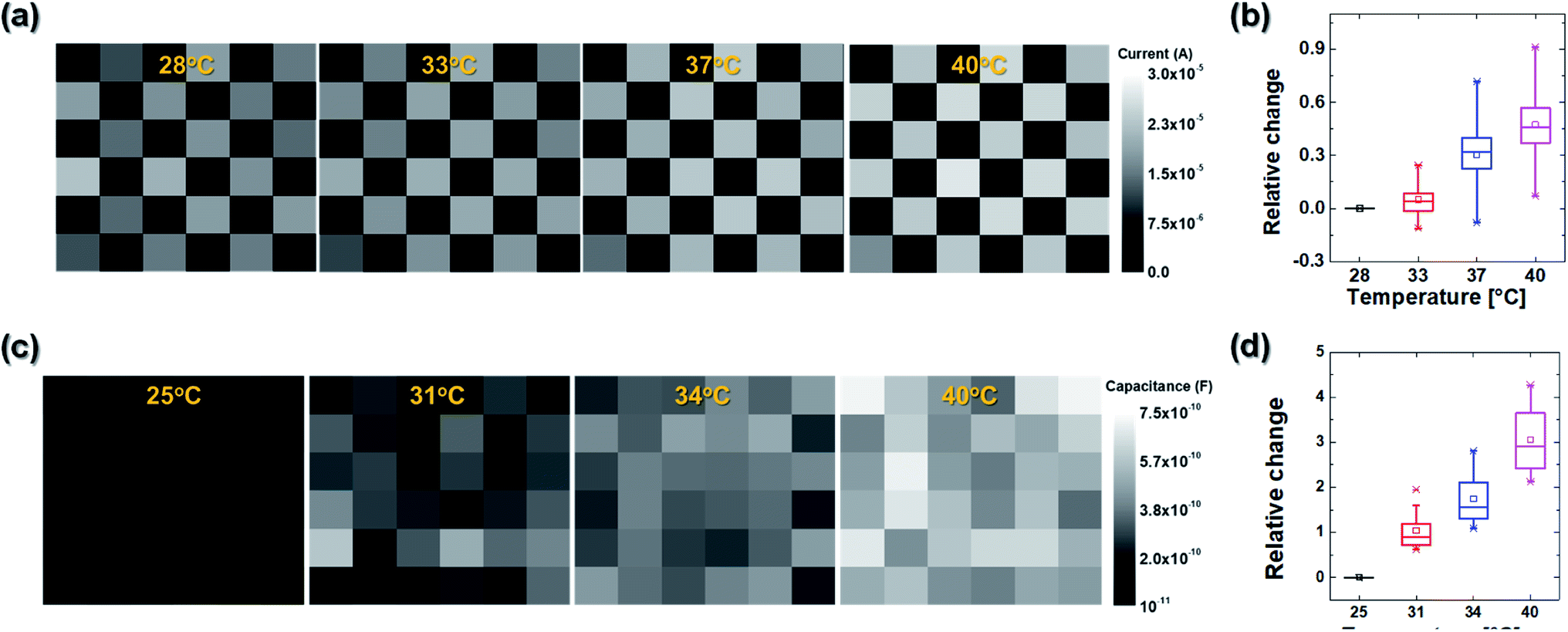 | ||
| Fig. 4 (a) Mapping of current with temperature on flat devices. (b) Summarizing current ITP data as relative change. (c) Mapping of capacitance with temperature on flat devices. (d) Summarizing capacitance ITP data as relative change. | ||
Fig. 4c shows the result of capacitance type array mapping. There is no discrimination compared to the resistance type, where the IMP and ITP are clearly distinguished. As mentioned earlier, this appears to be caused by the other pixels connected to the column and row lines, which act like parasite capacitance. This can be seen more clearly when the values of the pixels change with temperature. As the temperature is increased from 25 to 40 °C, the IMP increases to a similar range as that of the ITP, indicating that it is affected by the other pixels connected to the electrodes. The sensitivity is about 0.2/°C (it is also calculated in Fig. 4d). It can be seen that the results do not differ much from that of single devices. In other words, it is impossible to measure the exact value at each location in the array structure for the capacitance type sensor with ionic material.
Fig. 5a and b respectively show the optical image and mapping data that measure the current while bending the wrist when an array device is attached to acrylic gloves. It shows the experimental results of the three conditions when bending with the initial conditions, tilts of 30° and 60°. In the mapping shown in Fig. 2b, the top-left pixel is the FIMP, which becomes gray as the tilt angle increases. For TIMP, there is no significant change from 0° to 30°, but the current value appears to increase significantly with 60°. This is because the flexible PI is strained and tight, causing it to stick closely to the skin, thereby increasing the current of the device due to body temperature.
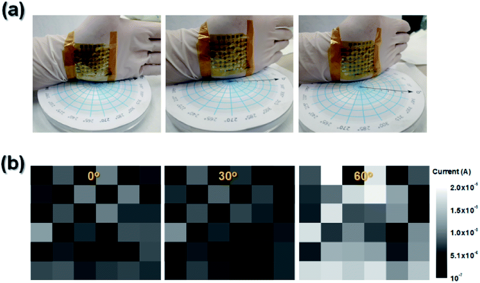 | ||
| Fig. 5 (a) Optical images under 3 conditions of angle of wrist flexion. (b) Mapping data of angle of wrist flexion. | ||
We tested how many times it repeats in the array structure in real time, using a bending machine. (ESI Fig. 4†). Fig. 6a was repeatedly folded and bloomed to measure how current of the FIMP and TIMP. In both cases, the current value was measured as the decay over time, which is a unique characteristic of the ionic TPU. The FIMP of the black line has 4- or 5-times relative change. On the other hand, the red line of TIMP shows that it is almost unaffected by the bending machine's movement. Fig. 6b shows that the measured on/off type sensor against pressure was maintained up to almost 1000 cycles during the repeated loading/unloading.
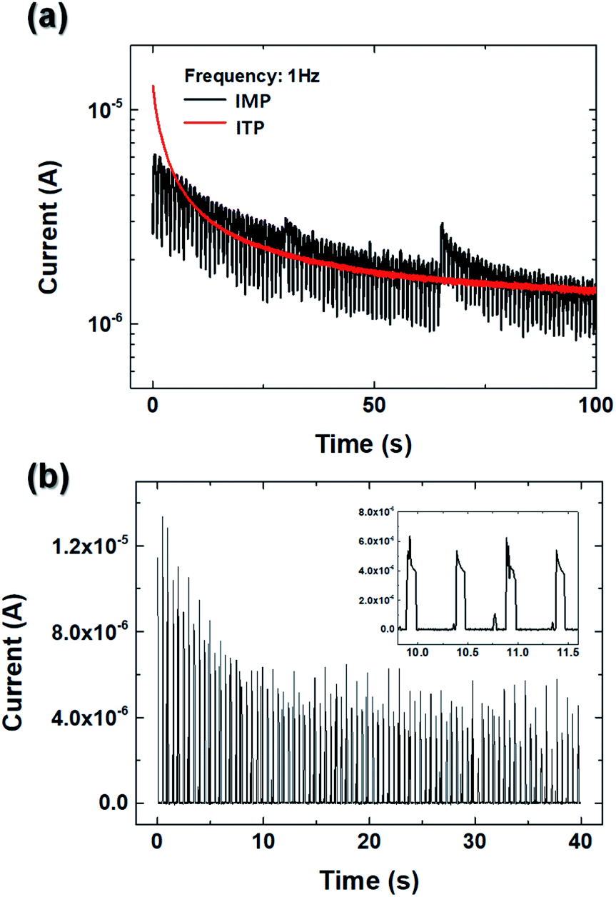 | ||
| Fig. 6 (a) Current of IMP and ITP under repeated flexion. (b) Durability test of IMP. | ||
4. Conclusion
We developed thermal and flexion sensors that can be applied to people and robots using i-TPU, which is an ionic polymer material. It is easy to fabricate because of the simple structures formed due to the properties of materials. The electrical characteristics were measured for each i-TPU sensor pixel. The temperature was measured by changing the intrinsic properties of the material, while flexion was measured using a method in which a pixel with a structurally low height is bent and touched. When measuring resistance (or current), both temperature and bending could achieve high sensitivity, and the noise signals from other pixels could be reduced, making it more suitable for array structures. On the other hand, capacitance type sensors vary linearly according to the temperature and bending radius, giving an advantage when measuring the exact values between them. In addition, the range of errors was low, which is advantageous in terms of reliability.Conflicts of interest
The authors have no conflicts of interest to declare.Acknowledgements
This work was supported by the National Research Foundation of Korea (NRF) grant funded by the Korea government (MSIT) (NRF-2017R1E1A1A01074087).References
- T. Liu, Y. Inoue and K. Shibata, Measurement, 2009, 42, 978–988 CrossRef.
- W. Gao, S. Emaminejad, H. Y. Y. Nyein, S. Challa, K. Chen, A. Peck, H. M. Fahad, H. Ota, H. Shiraki, D. Kiriya, D.-H. Lien, G. A. Brooks, R. W. Davis and A. Javey, Nature, 2016, 529, 509–514 CrossRef CAS PubMed.
- Y. Liu, M. Pharr and G. A. Salvatore, ACS Nano, 2017, 11, 9614–9635 CrossRef CAS PubMed.
- M. Amjadi, K.-U. Kyung, I. Park and M. Sitti, Adv. Funct. Mater., 2016, 26, 1678–1698 CrossRef CAS.
- H. Wang, B. Zhu, W. Jiang, Y. Yang, W. R. Leow, H. Wang and X. Chen, Adv. Mater., 2014, 26, 3638–3643 CrossRef CAS PubMed.
- T.-P. Huynh, P. Sonar and H. Haick, Adv. Mater., 2017, 29, 1604973 CrossRef PubMed.
- J. S. Lee, K.-Y. Shin, O. J. Cheong, J. H. Kim and J. Jang, Sci. Rep., 2015, 5, 7887 CrossRef CAS PubMed.
- C. Luo, J. Jia, Y. Gong, Z. Wang, Q. Fu and C. Pan, ACS Appl. Mater. Interfaces, 2017, 9, 19955–19962 CrossRef CAS PubMed.
- X.-H. Zhao, S.-N. Ma, H. Long, H. Yuan, C. Y. Tang, P. K. Cheng and Y. H. Tsang, ACS Appl. Mater. Interfaces, 2018, 10, 3986–3993 CrossRef CAS PubMed.
- A. Menzel, K. Subannajui, F. Güder, D. Moser, O. Paul and M. Zacharias, Adv. Funct. Mater., 2011, 21, 4342–4348 CrossRef CAS.
- Y. Yamamoto, S. Harada, D. Yamamoto, W. Honda, T. Arie, S. Akita and K. Takei, Sci. Adv., 2016, 2, e1601473 CrossRef PubMed.
- Z. Qian, X. Shan, L. Chai, J. Ma, J. Chen and H. Feng, ACS Appl. Mater. Interfaces, 2014, 6, 6797–6805 CrossRef CAS PubMed.
- V. C. R. Appel, V. L. Belini, D. H. Jong, D. V. Magalhães and G. A. P. Caurin, in 5th IEEE RAS/EMBS International Conference on Biomedical Robotics and Biomechatronics, 2014, pp. 276–280 Search PubMed.
- J. Engel, J. Chen, X. Wang, Z. Fan, L. Chang and D. Jones, in Proceedings 2003 IEEE/RSJ International Conference on Intelligent Robots and Systems (IROS 2003) (Cat. No. 03CH37453), 2003, vol. 3, pp. 2359–2364 Search PubMed.
- X. Wang, L. Dong, H. Zhang, R. Yu, C. Pan and Z. L. Wang, Adv. Sci., 2015, 2, 1500169 CrossRef PubMed.
- H. Wang, Z. Wang, J. Yang, C. Xu, Q. Zhang and Z. Peng, Macromol. Rapid Commun., 2018, 39, 1800246 CrossRef PubMed.
- Y. Wang, S. Gong, S. Jia Wang, G. P. Simon and W. Cheng, Mater. Horiz., 2016, 3, 208–213 RSC.
- N. N. Jason, M. D. Ho and W. Cheng, J. Mater. Chem. C, 2017, 5, 5845–5866 RSC.
- S. G. Yoon, B. J. Park and S. T. Chang, ACS Appl. Mater. Interfaces, 2017, 9, 36206–36219 CrossRef CAS PubMed.
- U. Khan, T.-H. Kim, H. Ryu, W. Seung and S.-W. Kim, Adv. Mater., 2017, 29, 1603544 CrossRef PubMed.
- Q. Wang, M. Jian, C. Wang and Y. Zhang, Adv. Funct. Mater., 2017, 27, 1605657 CrossRef.
- B. Nie, R. Li, J. Cao, J. D. Brandt and T. Pan, Adv. Mater., 2015, 27, 6055–6062 CrossRef CAS PubMed.
- Z. Lei, Q. Wang, S. Sun, W. Zhu and P. Wu, Adv. Mater., 2017, 29, 1700321 CrossRef PubMed.
- S. Jang, E. Jee, D. Choi, W. Kim, J. S. Kim, V. Amoli, T. Sung, D. Choi, D. H. Kim and J.-Y. Kwon, ACS Appl. Mater. Interfaces, 2018, 10, 31472–31479 CrossRef CAS PubMed.
- M. L. Jin, S. Park, J.-S. Kim, S. H. Kwon, S. Zhang, M. S. Yoo, S. Jang, H.-J. Koh, S.-Y. Cho, S. Y. Kim, C. W. Ahn, K. Cho, S. G. Lee, D. H. Kim and H.-T. Jung, Adv. Mater., 2018, 30, 1706851 CrossRef PubMed.
- M. L. Jin, S. Park, Y. Lee, J. H. Lee, J. Chung, J. S. Kim, J.-S. Kim, S. Y. Kim, E. Jee, D. W. Kim, J. W. Chung, S. G. Lee, D. Choi, H.-T. Jung and D. H. Kim, Adv. Mater., 2017, 29, 1605973 CrossRef PubMed.
- T. Ganley, D. L. S. Hung, G. Zhu and X. Tan, IEEE/ASME Transactions on Mechatronics, 2011, 16, pp. 80–89 Search PubMed.
- P. Brunetto, L. Fortuna, P. Giannone, S. Graziani and S. Strazzeri, IEEE Trans. Instrum. Meas., 2011, 60, 2951–2959 Search PubMed.
- S. Nakata, T. Arie, S. Akita and K. Takei, ACS Sens., 2017, 2, 443–448 CrossRef CAS PubMed.
- S. Y. Hong, Y. H. Lee, H. Park, S. W. Jin, Y. R. Jeong, J. Yun, I. You, G. Zi and J. S. Ha, Adv. Mater., 2016, 28, 930–935 CrossRef CAS PubMed.
- T. Q. Trung, S. Ramasundaram, B.-U. Hwang and N.-E. Lee, Adv. Mater., 2016, 28, 502–509 CrossRef CAS PubMed.
- J. Vatamanu, L. Xing, W. Li and D. Bedrov, Phys. Chem. Chem. Phys., 2014, 16, 5174–5182 RSC.
- V. Ivaništšev, A. Ruzanov, K. Lust and E. Lust, J. Electrochem. Soc., 2013, 160, H368–H375 CrossRef.
- A. Kisza, Electrochim. Acta, 2006, 51, 2315–2321 CrossRef CAS.
- V. Lockett, M. Horne, R. Sedev, T. Rodopoulos and J. Ralston, Phys. Chem. Chem. Phys., 2010, 12, 12499–12512 RSC.
Footnote |
| † Electronic supplementary information (ESI) available. See DOI: 10.1039/c9ra08188g |
| This journal is © The Royal Society of Chemistry 2019 |