
 Open Access Article
 This Open Access Article is licensed under a Creative Commons Attribution-Non Commercial 3.0 Unported Licence
Ultralow lattice thermal conductivity and high thermoelectric performance of monolayer KCuTe: a first principles study
Jinjie Gu *,
Lirong Huang and
Shengzong Liu
*,
Lirong Huang and
Shengzong Liu
Hunan Provincial Key Laboratory of Finance & Economics Big Data Science and Technology, School of Information Technology and Management, Hunan University of Finance and Economics, Changsha 410205, P. R. China. E-mail: gujinjie_HUFE@163.com
First published on 7th November 2019
Abstract
Monolayer KCuTe is a new-type of two-dimensional (2D) semiconductor material with high carrier mobility and large power energy conversion efficiencies, suggesting its potential application in thermoelectric (TE) and photoelectric fields. Based on the density functional theory (DFT) and semiclassical Boltzmann transport equation, the electronic and phonon transport properties of monolayer KCuTe are systematically studied. Our results show that it possesses an ultralow lattice thermal conductivity value of nearly ∼0.13 W m−1 K−1 at 300 K, mainly attributed to its small phonon group velocity, large Grüneisen parameters, and strong phonon–phonon scattering. Furthermore, the intralayer opposite phonon vibrations greatly restrict the heat transport. Monolayer KCuTe shows an ideal direct band gap of ∼1.21 eV, and a high twofold degeneracy appearing at the Γ point gives a high Seebeck coefficient of ∼2070 μV K−1, leading to high TE performance. Using the transport coefficients together with constant electron relaxation time, the figure of merit (ZT) can reach 2.71 at 700 K for the p-type doping, which is comparable to the well-known TE material SnSe (2.6 ± 0.3 at 935 K). Our theoretical studies may provide perspectives to TE applications of monolayer KCuTe and stimulate further experimental synthesis.
1 Introduction
With the depletion of the fossil fuels, searching for renewable energy resources as well as related materials is urgently demanded. In particular, TE materials have attracted much attention, because they could convert waste heat into electric energy via the Seebeck effect.1,2 In general, the conversion efficiency of a TE material is characterized by the dimensionless figure of merit ZT3
 | (1) |
It is well known that TE materials with plicated layered configuration such as SnSe,11 PbTe,12 and Bi2Te3 (ref.13) have low thermal conductivity, which is one of the key factors to achieve good TE performance. Usually, the most pristine TE materials are composed of light atoms and heavy atoms, all of which possess strong anharmonicity.14–16 For instance, Bi2O2Se monolayer, a new star material, exhibits an intrinsically low thermal conductivity (0.74 W m−1 K−1 at 300 K) due to its strong anharmonic interaction.17 For the phosphorene-like SnSe compound, its characteristic crystal structure and electronic structure lead to low κl and high power factor.11 With the excellent electrical transport properties, the deceptively simple material SnSe monolayer shows an unexpectedly high ZT of 2.76 at 700 K and it has become a very promising TE material.18
Very recently, the monolayer KCuTe, as a novel layered material, has been theoretically proposed,19 which can be prepared by isovalent substitutions in layered KAgSe. The monolayer KCuTe has a favorable direct band gap with ultrahigh electron mobility of 1.3 × 104 cm2 V−1 s−1, which is not only much larger than that of the MoS2 monolayer20 but also can be on a par with that of black phosphorene (1.0–2.6 × 104 cm2 V−1 s−1).21 Further, its excellent electrical properties, large power energy conversion efficiencies (∼21.5%) and applicable band gap, offer multiple perspectives for applications in photoelectric and photovoltaic solar cells.19 Considering these outstanding performances, it is necessary to study comprehensively on its TE properties. Based on theoretical calculations, we systematically study the TE properties of monolayer KCuTe. Meanwhile, we find that it exhibits a high Seebeck coefficient of 2070 μV K−1 and an ultralow lattice thermal conductivity of 0.13 W m−1 K−1, which are prerequisites for achieving high TE performance. Detailed discussions of phonon spectrums, atomic vibration modes, phonon group velocity, and Grüneisen parameters are presented to explain its heat transport ability. The maximum ZT value is as high as 2.71 at 700 K for p-type doping. It is revealed that the monolayer KCuTe possesses extraordinary TE response.
2 Computational methods
Within the framework of DFT, the electronic properties of monolayer KCuTe were investigated by using the projector augmented wave method, which was implemented in the Vienna ab initio Simulation Package (VASP).22 The generalized gradient approximation (GGA)23 in the Perdew–Burke–Ernzerhof (PBE)24 was employed. The cutoff energy of the plane wave was set as 500 eV and 11 × 11 × 1 Monkhorst–Pack k-mesh were adopted in the calculations. A vacuum region of 25 Å was set along the z direction to avoid the interactions between periodic layers. The semi-empirical DFT-D3 (ref. 25) correction was included to evaluate the van der Waals interactions. The atomic positions are fully relaxed with the Hellman–Feynman force 0.01 eV Å−1, while the total energy convergence criteria was 10−5 eV Å−1. The optimized lattice parameter of monolayer KCuTe is a = 4.26 Å, which is consistent with the previous theoretical prediction.19 In order to calculate its electronic structure, the hybrid functional approach of Heyd–Scuseria–Ernzerhof (HSE06) was employed.26 By using the Boltzmann transport theory and the rigid band approach, the electronic transport properties were obtained, implemented in the BoltzTraP code.27 The constant relaxation time approximation was employed, which was valid because the relaxation time doesn't vary strongly within the energy scale of kBT.28 Such method has accurately assessed TE properties of many materials.29 To accurately perform Fourier interpolation of the Kohn–Sham eigenvalues, a dense 45 × 45 × 1 k-mesh was employed in the Brillouin zone (BZ).Using the ShengBTE code,30 the phonon transport properties were evaluated. The harmonic second-order interaction force constants (2nd IFCs) and phonon spectrum were obtained by the VASP and Phonopy packages31 using 5 × 5 × 1 supercell with 3 × 3 × 1 k-mesh. The anharmonic third-order IFCs (3rd IFCs) were obtained using the finite-difference method,32 where the influence of the seventh nearest neighbors is considered. Additionally, the convergence of the κl as a function of the k-mesh was carefully tested. A dense 35 × 35 × 1 k-mesh was employed for the calculation of the lattice thermal conductivity. In order to convert conductance of monolayer material to conductivity, the effective thickness of 7.8 Å was chosen in monolayer KCuTe.
3 Results and discussions
3.1 Electronic structures
The monolayer KCuTe shows an orthorhombic structure with the space group P4/nmm symmetry (129), as shown in Fig. 1(a) and (b). We can see clearly that the monolayer KCuTe exhibits five atomic-layers in the form of K–Cu–Te–Cu–K and six atoms per unit cell, which greatly increases the complexity of the structure. Moreover, its conspicuously plicated configuration can give rise to strong lattice vibrations, greatly suppressing phonon transport ability.17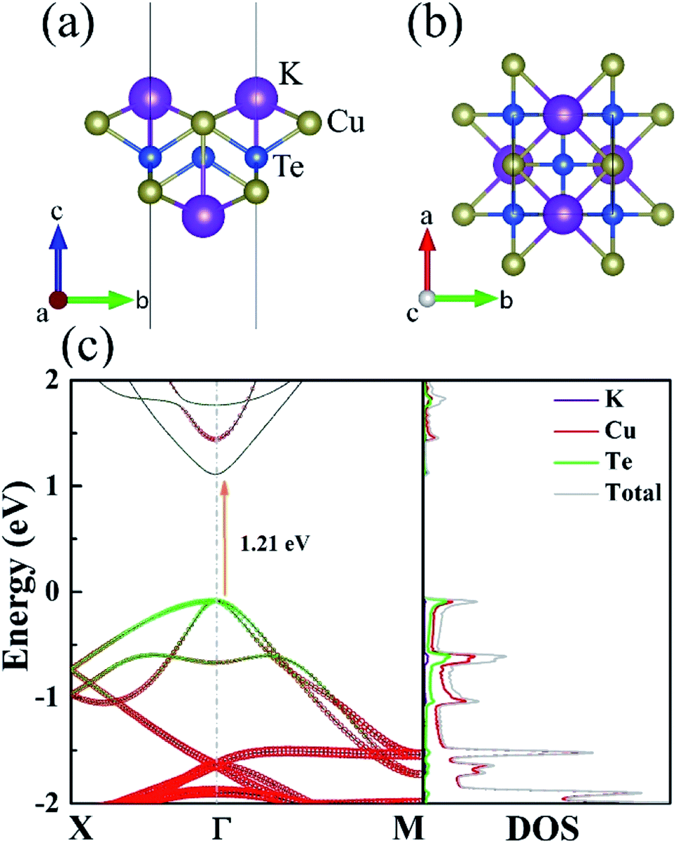 | ||
| Fig. 1 Side (a) and top (b) views of the atomic structure of monolayer KCuTe. (c) The band structures and the corresponding DOS. | ||
The band structures and corresponding projected density of state (DOS) of monolayer KCuTe along a series of high symmetry points in the BZ are shown in Fig. 1(c). It has direct band gap with the valence band maximum (VBM) and conduction band minimum (CBM) locating at Γ point. In the vicinity of Fermi level, the conduction bands (CB) are rarely occupied by the K, Cu and Te atoms, whereas the valence bands (VB) are primarily contributed by the Cu and Te atoms. Interestingly, a twofold degeneracy could be observed at Γ point. It is reported that band degeneracy has been proved to be critical for achieving high TE performance33,34 and can be realized through proper band engineering.35 In addition, this degenerated electronic state is relatively flat at the VB edge, which is in favour of high PF.36 Several sharp peaks are observed at VB in DOS, a signal of a dramatic increase in Seebeck coefficients.37,38 Therefore, unique DOS structure and an intrinsic VB degeneracy appear together in the monolayer KCuTe, which are good electronic features for high-performance of TE equipments.
3.2 Electron transport properties
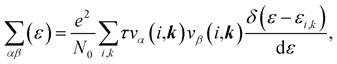
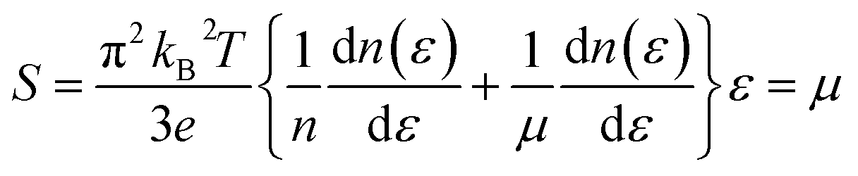
With the constant relaxation time assumption, the electronic transport properties for KCuTe are obtained. Here, we computed the Seebeck coefficients S, electrical conductivity κl, and electronic thermal conductivity κe, and PF S2σ of monolayer KCuTe under the temperature from 300 to 700 K. Calculative results are shown in Fig. 2(a)–(d) as a function of chemical potential μ, of which the positive and negative side correspond to n-type and p-type doping, respectively. By using the Boltzmann transport theory, the S and σ could be expressed as27
 | (2) |
 | (3) |
 | (4) |
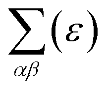 is the transport distribution function. As shown in Fig. 2(a), the monolayer KCuTe exhibits relatively large values of the Seebeck coefficients. At room temperature, the Seebeck coefficients can reach to 2070 and 1970 μV K−1 for p- and n-type doping. Meanwhile, we can also find that the Seebeck coefficient for n-type doping is slightly larger than that of the p-type doping, which can attribute to its DOS. As has been reported,35 the multiple degeneracy usually significantly improve the Seebeck coefficient. We can clearly find that the Seebeck coefficients exhibit the obvious temperature-dependent behavior. At low chemical potentials, the Seebeck coefficients appear peaks due to the sharp energy dependence of the total DOS, i.e., large ∂n(ε)/∂(ε), as shown in Fig. 1. For doping system, the Seebeck coefficients could be derived according to the Mott relation39
 | (5) |
 | ||
| Fig. 2 (a) Seebeck coefficients, (b) electrical conductivity, (c) electronic thermal conductivity, and (d) power factor with respect to the scattering time at different temperatures (300, 500, and 700 K) as functions of the chemical potential. | ||
We can find that the Seebeck coefficient can be further enhanced by optimizing the carrier concentration.
The electrical conductivity σ/τ as a function of chemical potential is shown in Fig. 2(b). In fact, theoretical calculations prove that the p-type doping shows larger σ/τ than that of the n-type ones. The slopes of the σ/τ around the VBM and CBM is flatted by increasing temperature because the electrons obey the Fermi–Dirac distribution.
Besides, the electronic thermal conductivity κe can be calculated by using the Wiedemann–Franz law:40
| κe = LσT, | (6) |
3.3 Phonon transport properties
The phonon dispersions and partial atomic phonon density of states (PhDOS) of monolayer KCuTe are shown in Fig. 3(a). Since the acoustic branches play a major contribution to heat transport,41 we highlight these phonon modes with different colors. Here, the negative phonon frequency is not observed, demonstrating its dynamical stability. Surprising, we can find that it shows a very narrow phonon frequency interval with the maximum frequency of the optical mode about 4.5 THz. Such low phonon frequencies are beneficial to low thermal conductivity. Additionally, its lowest optical mode frequency is as low as 0.39 THz, which is much lower than that of the phosphorene like SnSe (0.99 THz).42 We can also find that the lowest optical modes are overlapping with its acoustic branches, resulting in strong acoustic–optical interactions and low lattice thermal conductivity. From the corresponding PhDOS, we can see that the phonon branches are evenly occupied by K, Cu and Te atoms in the full-frequency region, which further verify its stability.43 This phenomenon can attribute to the strongly overlapping electron states. The out-of-plan acoustic mode (ZA) has parabolic dispersion, which is a unique character for atomically thin materials. We can note that these flat phonon modes and protuberant PhDOS can give rise to small phonon velocities.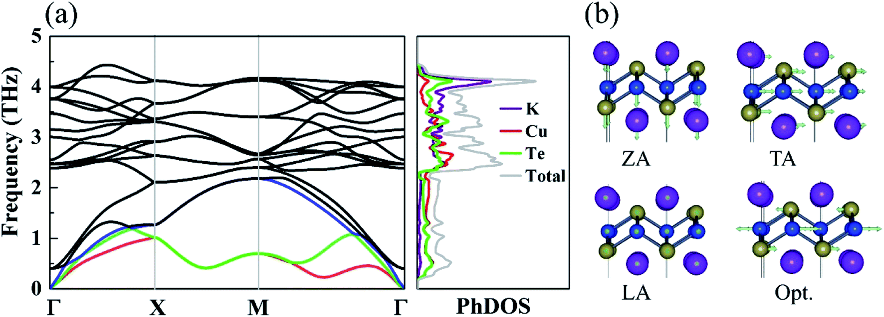 | ||
| Fig. 3 (a) Phonon dispersion and total and partial phonon density of states (PhDOS) of monolayer KCuTe. (b) The corresponding vibrational modes of the acoustic phonon branches (the red, green and blue lines corresponding to the ZA, TA, and LA) and the lowest optical branch (Opt.) near and at Γ point. | ||
To further study each modes phonon spectrum, some typical vibration modes of KCuTe sheet at Γ point are shown in Fig. 3(b). One can see clearly that the vibrations of the acoustic modes are strictly along the in-plane (LA and TA) or out-of-plane (TA), which are an inherent vibration property. For the lowest optical branch, we find that the upper Cu atoms move in opposite directions with respect to the lower Cu atoms, including both intralayer Se atoms, while the K atoms keep still. Such atomic vibration mode will greatly suppress heat transport ability in layered materials. Similar with graphene,44 these optical modes are easily thermally activated at room temperature, leading to low thermal conductivity via enhancing phonon–phonon scattering.45
From the phonon kinetic theory, the lattice thermal conductivity in a solid is defined by
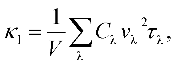 | (7) |
The phonon velocity is a very important physical parameter for the calculation of thermal conductivity. It can be obtained by using the phonon spectrum,
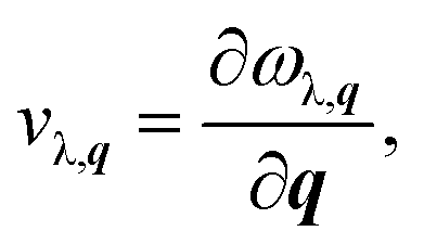 | (8) |
Besides the phonon velocities, we further study its Grüneisen parameters and phonon relaxation time of each phonon modes, as shown in Fig. 4(c) and (d). The Grüneisen parameters can qualitatively describe the anharmonic interactions of a crystal. In general, it can be computed from the relationship between phonon frequency and volume change as below:
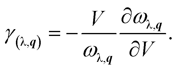 | (9) |
Usually, a large |γ| means that it might have a strong phonon–phonon anharmonic scattering. Surprisingly, we can see clearly that the monolayer KCuTe exhibits very large Grüneisen parameters, indicating that it possesses strong anharmonicity. From the Fig. 4(c), we find that the Grüneisen parameter of ZA mode is much larger than that of the TA and LA mode. Herein, the phonon relaxation time can be obtained by the summation of various scattering processes.48 Compared with some common TE materials,17,41 we can see clearly that it shows a very short relaxation time (nearby 0.1 ps), leading to low lattice thermal conductivity. To further analyze its phonon relaxation time, the three phonon scattering phase space (P3) is presented as shown in the insert of Fig. 4(c). One can see that the monolayer KCuTe possesses a relatively larger P3 in the full-frequency region, which indicates that it exists strong phonon–phonon scattering and greatly suppress the phonon transport.
3.4 Thermoelectric figure of merit
Using the electronic and phonon transport coefficients available, we have computed the TE properties of monolayer KCuTe. Herein, the electronic scattering time τ is 3.5 fs, extracted from previous report.49 The ZT values with respect to chemical potential and carrier concentration at 300, 500 and 700 K are shown in Fig. 5(a) and (b). Additionally, we can see that the ZT of the p-type doping is higher that of the n-type doping, which can attribute to the difference of PF. With the temperature increasing, the peak becomes wider and the peak position moves toward μ = 0. We can see that the ZT values can approach 2.71 and 1.51 for p-type and n-type doping at 700 K since it has a lower thermal conductivity. Moreover, the corresponding concentration of maximum ZT is about 5 × 1011 cm−2 for p-type doping.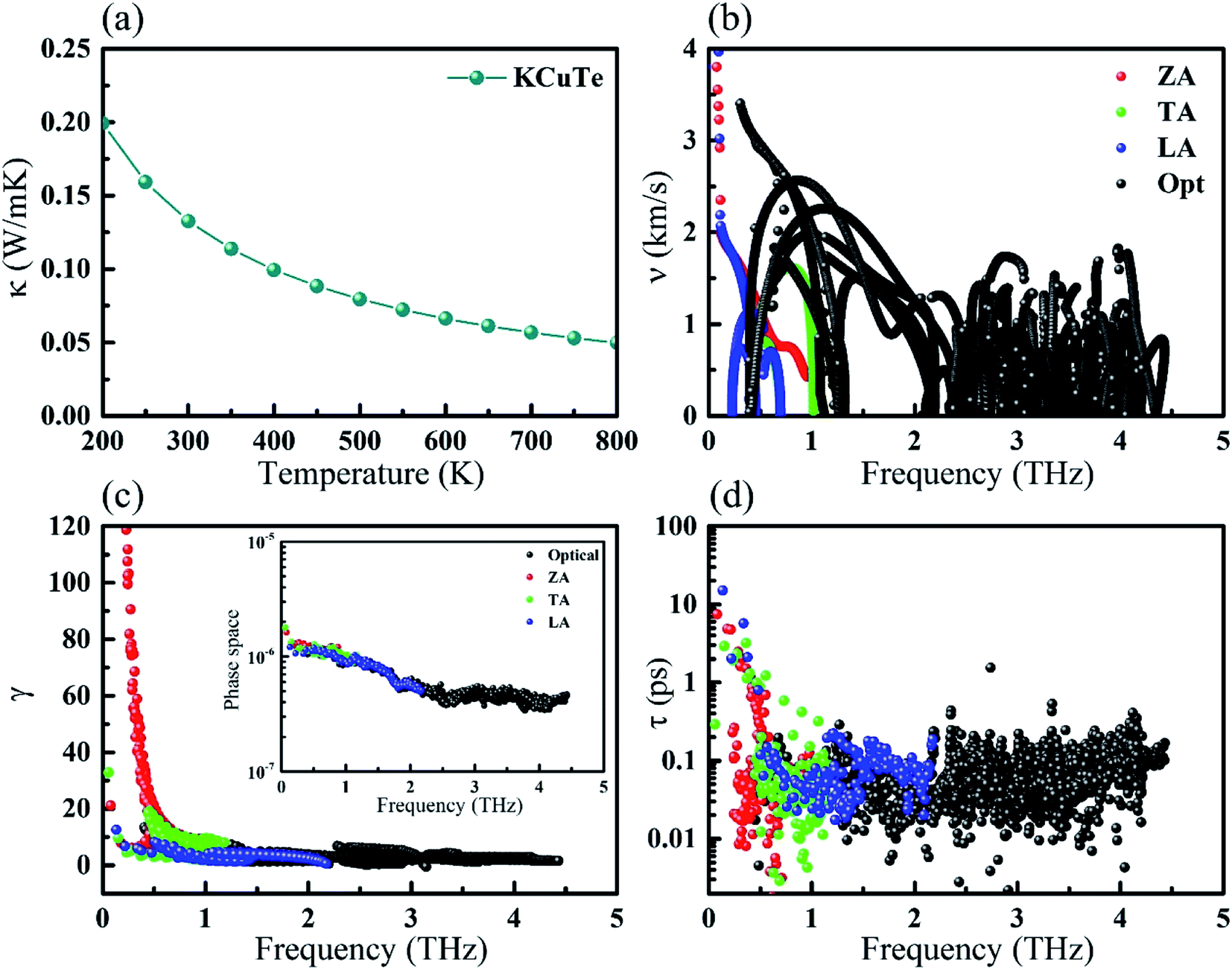 | ||
| Fig. 4 (a) Calculated lattice thermal conductivity with respect to temperature for monolayer KCuTe. (b) Phonon group velocity, (c) Grüneisen parameters, and (d) phonon relaxation time at 300 K. The inset of (c) is three phonon phase space. | ||
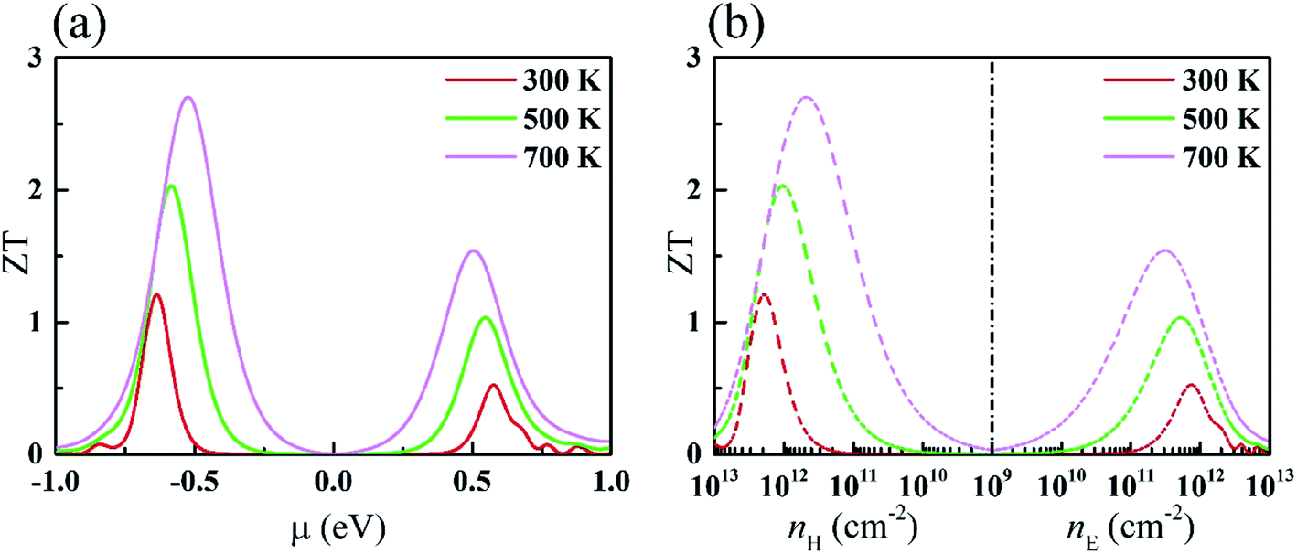 | ||
| Fig. 5 ZT with respect to (a) chemical potential and (b) carrier concentration for monolayer KCuTe. | ||
4 Conclusion
In summary, using DFT and Boltzmann transport equation, we systematically studied the electronic and phonon transport properties of monolayer KCuTe. Results show that it possesses an ideal band gad (1.21 eV) with a high Seebeck coefficients of 2070 μV K−1 at room temperature. Since the multiple valley degeneracy around VB, it exhibits outstanding electrical transport properties. Additionally, its unique crystal texture, small phonon velocity, large Grüneisen parameters, and short phonon relaxation time greatly suppress the heat transport ability, leading to ultralow lattice thermal conductivity of 0.13 W m−1 K−1 at 300 K. The ZT of monolayer KCuTe is as high as 2.71 at 700 K for p-type doping. Collectively, our works demonstrate that the monolayer KCuTe possesses excellent TE performance and will become a hopeful candidate in TE material field.Conflicts of interest
There are no conflicts to declare.Acknowledgements
This work was supported by the Research project of Education Department of Hunan Province (No. 18A441, 18C0958), and the Open Research Fund of Hunan Provincial Key Laboratory of Network Investigational Technology (No. 2017WLZC006), and the Key Project of Educational Planning of Hunan Province (No. XJK18DJA1).References
- S. Chu, Y. Cui and N. Liu, Nat. Mater., 2017, 16, 16–22 CrossRef.
- M. Aneke and M. Wang, Appl. Energy, 2016, 179, 350–377 CrossRef.
- J. Yang, L. Xi, W. Qiu, L. Wu, X. Shi, L. Chen, J. Yang, W. Zhang, C. Uher and D. J. Singh, npj Comput. Mater., 2016, 2, 15015 CrossRef CAS.
- J. M. Skelton, S. C. Parker, A. Togo, I. Tanaka and A. Walsh, Phys. Rev. B: Condens. Matter Mater. Phys., 2014, 89, 205203 CrossRef.
- Z. Wang, L. Zhao, K. F. Mak and J. Shan, Nano Lett., 2017, 17, 740–760 CrossRef CAS.
- L.-P. Tang, L.-M. Tang, H. Geng, Y.-P. Yi, Z. Wei, K.-Q. Chen and H.-X. Deng, Appl. Phys. Lett., 2018, 112, 012101 CrossRef.
- D. Li, J. He, G. Ding, Q. Tang, Y. Ying, J. He, C. Zhong, Y. Liu, C. Feng and Q. Sun, et al., Adv. Funct. Mater., 2018, 28, 1801685 CrossRef.
- Y.-Y. Liu, Y.-J. Zeng, P.-Z. Jia, X.-H. Cao, X. Jiang and K.-Q. Chen, J. Phys.: Condens. Matter, 2018, 30, 275701 CrossRef PubMed.
- X. Y. Mi, X. Yu, K. L. Yao, X. Huang, N. Yang and J. T. Lü, Nano Lett., 2015, 15, 5229–5234 CrossRef CAS.
- G. Xie, D. Ding and G. Zhang, Adv. Phys.: X, 2018, 3, 1480417 Search PubMed.
- L. D. Zhao, S. H. Lo, Y. Zhang, H. Sun, G. Tan, C. Uher, C. Wolverton, V. P. Dravid and M. G. Kanatzidis, Nature, 2014, 508, 373–377 CrossRef CAS.
- J. P. Heremans, V. Jovovic, E. S. Toberer, A. Saramat, K. Kurosaki, A. Charoenphakdee, S. Yamanaka and G. J. Snyder, Science, 2008, 321, 554–557 CrossRef CAS.
- M. Scheele, N. Oeschler, K. Meier, A. Kornowski, C. Klinke and H. Weller, Adv. Funct. Mater., 2009, 19, 3476–3483 CrossRef CAS.
- G. Xie, Z. Ju, K. Zhou, X. Wei, Z. Guo, Y. Cai and G. Zhang, npj Comput. Mater., 2018, 4, 21 CrossRef.
- X. Yu, C. Cheng, Y. Pei, W. Di, K. Peng, X. Zhou, S. Gong, J. He, Y. Zhang and Z. Zhi, Phys. Rev. B: Condens. Matter Mater. Phys., 2016, 94, 125203 CrossRef.
- C. W. Li, O. Hellman, J. Ma, A. F. May, H. B. Cao, X. Chen, A. D. Christianson, G. Ehlers, D. J. Singh and B. C. Sales, Phys. Rev. Lett., 2014, 112, 175501 CrossRef CAS PubMed.
- X.-L. Zhu, P.-F. Liu, G. Xie and B.-T. Wang, Phys. Chem. Chem. Phys., 2019, 21, 10931–10938 RSC.
- F. Q. Wang, S. Zhang, J. Yu and Q. Wang, Nanoscale, 2015, 7, 15962–15970 RSC.
- W. Xu, R. Wang, B. Zheng, X. Wu and H. Xu, ACS Appl. Mater. Interfaces, 2019, 11, 14457–14462 CrossRef CAS.
- S. Kim, A. Konar, W.-S. Hwang, J. H. Lee, J. Lee, J. Yang, C. Jung, H. Kim, J.-B. Yoo and J.-Y. Choi, et al., Nat. Commun., 2012, 3, 1011 CrossRef.
- J. Qiao, X. Kong, Z.-X. Hu, F. Yang and W. Ji, Nat. Commun., 2014, 5, 4475 CrossRef CAS.
- G. Kresse and J. Furthmüller, Phys. Rev. B: Condens. Matter Mater. Phys., 1996, 54, 11169 CrossRef CAS.
- P. E. Blöchl, Phys. Rev. B: Condens. Matter Mater. Phys., 1994, 50, 17953 CrossRef.
- G. Kresse and D. Joubert, Phys. Rev. B: Condens. Matter Mater. Phys., 1999, 59, 1758–1775 CrossRef CAS.
- N. Marom, A. Tkatchenko, M. Rossi, V. V. Gobre, O. Hod, M. Scheffler and L. Kronik, J. Chem. Theory Comput., 2011, 7, 3944–3951 CrossRef CAS.
- J. Heyd, G. E. Scuseria and M. Ernzerhof, J. Chem. Phys., 2003, 118, 8207–8215 CrossRef CAS.
- G. K. H. Madsen and D. J. Singh, Comput. Phys. Commun., 2006, 175, 67–71 CrossRef CAS.
- L. Chaput, P. Pécheur and C. Scherrer, Phys. Rev. B: Condens. Matter Mater. Phys., 2007, 75, 045116 CrossRef.
- D. Parker and D. J. Singh, Phys. Rev. B: Condens. Matter Mater. Phys., 2010, 82, 035204 CrossRef.
- W. Li, J. Carrete, N. A. Katcho and N. Mingo, Comput. Phys. Commun., 2014, 185, 1747–1758 CrossRef CAS.
- A. Togo, F. Oba and I. Tanaka, Phys. Rev. B: Condens. Matter Mater. Phys., 2008, 78, 134106 CrossRef.
- W. Li, L. Lindsay, D. A. Broido, D. A. Stewart and N. Mingo, Phys. Rev. B: Condens. Matter Mater. Phys., 2012, 86, 174307 CrossRef.
- L. D. Zhao, V. P. Dravid and M. G. Kanatzidis, Energy Environ. Sci., 2014, 7, 251–268 RSC.
- X. L. Zhu, P. F. Liu, G. Xie, W. X. Zhou, B. T. Wang and G. Zhang, Nanomaterials, 2019, 9, 597 CrossRef CAS.
- Z. M. Gibbs, F. Ricci, G. Li, H. Zhu, K. Persson, G. Ceder, G. Hautier, A. Jain and G. J. Snyder, npj Comput. Mater., 2017, 3, 8 CrossRef.
- C. Fu, H. Wu, Y. Liu, J. He, X. Zhao and T. Zhu, Adv. Sci., 2016, 3, 1600035 CrossRef.
- H. Peng, N. Kioussis and G. J. Snyder, Phys. Rev. B: Condens. Matter Mater. Phys., 2014, 89, 195206 CrossRef.
- G. Ding, C. Wang, G. Gao, K. Yao, C. Dun, C. Feng, D. Li and G. Zhang, Nanoscale, 2018, 10, 7077–7084 RSC.
- J. P. Heremans, Acta Phys. Pol., A, 2005, 108, 609–634 CrossRef CAS.
- M. Jonson and G. Mahan, Phys. Rev. B: Condens. Matter Mater. Phys., 1980, 21, 4223 CrossRef CAS.
- P.-F. Liu, T. Bo, J. Xu, W. Yin, J. Zhang, F. Wang, O. Eriksson and B.-T. Wang, Phys. Rev. B, 2018, 98, 235426 CrossRef CAS.
- C. W. Li, J. Hong, A. F. May, D. Bansal, S. Chi, T. Hong, G. Ehlers and O. Delaire, Nat. Phys., 2015, 11, 1063 Search PubMed.
- T. Ouyang, E. Jiang, C. Tang, J. Li, C. He and J. Zhong, J. Mater. Chem. A, 2018, 6, 21532–21541 RSC.
- C. H. Lui and T. F. Heinz, Phys. Rev. B: Condens. Matter Mater. Phys., 2013, 87, 121404 CrossRef.
- J. Ding, B. Xu, Y. Lin, C. Nan and W. Liu, New J. Phys., 2015, 17, 083012 CrossRef.
- G. Xie, Y. Guo, X. Wei, K. Zhang, L. Sun, J. Zhong, G. Zhang and Y. W. Zhang, Appl. Phys. Lett., 2014, 104, 233901 CrossRef.
- M. M. Mahmoud, E. K. Rugut, M. P. Molepo and D. P. Joubert, Eur. Phys. J. B, 2019, 92, 87 CrossRef.
- K. Hess, Appl. Phys. Lett., 1979, 35, 484–486 CrossRef CAS.
- A. Parveen and G. Vaitheeswaran, Sci. Rep., 2018, 8, 13071 CrossRef.
| This journal is © The Royal Society of Chemistry 2019 |