
 Open Access Article
 This Open Access Article is licensed under a Creative Commons Attribution-Non Commercial 3.0 Unported Licence
Interface tailoring through the supply of optimized oxygen and hydrogen to semiconductors for highly stable top-gate-structured high-mobility oxide thin-film transistors†
Jong Beom Ko a,
Seung-Hee Leea,
Kyung Woo Parkb and
Sang-Hee Ko Park*a
a,
Seung-Hee Leea,
Kyung Woo Parkb and
Sang-Hee Ko Park*a
aDepartment of Materials Science and Engineering, Korea Advanced Institute of Science and Technology (KAIST), 291 Daehak-ro, Yuseong-gu, Daejeon 34141, Republic of Korea. E-mail: shkp@kaist.ac.kr
bSamsung Display, Co. Ltd., 1 Samsung-ro, Yongin-si, Gyeonggi-do 17113, Republic of Korea
First published on 7th November 2019
Abstract
Self-aligned structured oxide thin-film transistors (TFTs) are appropriate candidates for use in the backplanes of high-end displays. Although SiNx is an appropriate candidate for use in the gate insulators (GIs) of high-performance driving TFTs, direct deposition of SiNx on top of high-mobility oxide semiconductors is impossible due to significant hydrogen (H) incorporation. In this study, we used AlOx deposited by thermal atomic layer deposition (T-ALD) as the first GI, as it has good H barrier characteristics. During the T-ALD, however, a small amount of H from H2O can also be incorporated into the adjacent active layer. In here, we performed O2 or N2O plasma treatment just prior to the T-ALD process to control the carrier density, and utilized H to passivate the defects rather than generate free carriers. While the TFT fabricated without plasma treatment exhibited conductive characteristics, both O2 and N2O plasma-treated TFTs exhibited good transfer characteristics, with a Vth of 2 V and high mobility (∼30 cm2 V−1 s−1). Although the TFT with a plasma-enhanced atomic layer deposited (PE-ALD) GI exhibited reasonable on/off characteristics, even without any plasma treatment, it exhibited poor stability. In contrast, the O2 plasma-treated TFT with T-ALD GI exhibited outstanding stability, i.e., a Vth shift of 0.23 V under positive-bias temperature stress for 10 ks and a current decay of 1.2% under current stress for 3 ks. Therefore, the T-ALD process for GI deposition can be adopted to yield high-mobility, high-stability top-gate-structured oxide TFTs under O2 or N2O plasma treatment.
Introduction
Amorphous oxide semiconductors (AOSs) are appropriate candidates for the active layers of thin-film transistors (TFTs) due to their numerous advantages, such as high electron mobility, good electrical stability, uniformity over a large area, and easy fabrication.1–4 Therefore, oxide TFTs are considered the best candidates for use in the backplanes of large-area flat-panel displays (FPDs). Among the various FPDs, those based on active-matrix organic light-emitting diodes (AMOLEDs) and micro-light-emitting diodes (micro-LEDs) have attracted much attention due to their unique advantages, such as vivid color, high efficiency, and fast response times.5,6 In particular, they have excellent contrast, and their thinness and lightness make them suitable for use in wall and window displays. Therefore, they are promising candidates for next-generation AM displays with large sizes, high resolutions, and foldability. However, there are many important issues in terms of backplane that should be addressed before AMOLEDs and active matrix micro-LEDs can be used for higher resolution, larger-sized displays. The high mobility of TFTs is essential for fully charging capacitors in a short time. Hence, there is much current research on oxide TFTs with various types of high-mobility materials, such as indium zinc oxide (IZO),7 indium oxide (InO),8 zinc oxynitride (ZnON)9 and Al-doped ITZO (Al:ITZO).10 Furthermore, among low resistivity metal materials, copper (Cu) should generally be used for electrodes to reduce resistive–capacitive (RC) delay in the pixel arrays of large-sized, high-resolution displays.11,12Among the various TFTs, self-aligned (SA) TFTs are the most suitable for driving large-sized, high-resolution displays, due to their small parasitic capacitance.13 Therefore, we can increase the capacitance of gate insulators (GIs) in SA TFTs to realize large driving currents. In other words, we can obtain high trans-conductance values, which vary in proportion to the capacitance of the GI. High-k dielectric materials, such as HfO2,14 Y2O3,15 Si3N4, and Al2O3 (ref. 16) are good candidates for GIs.17 Among these, SiNx deposited by plasma-enhanced chemical vapor deposition (PE-CVD) is a suitable candidate for GIs of SA TFTs using Cu electrodes for display applications, because it has both high capacitance and good Cu diffusion barrier characteristics.18,19 Unfortunately, it is difficult to use SiNx as a GI for SA oxide TFTs, because hydrogen (H) is readily incorporated into the channel during GI deposition, thus increasing the carrier density and shifting turn-on voltage (Von) in the negative direction.18 As a solution, an H barrier layer can be introduced as a first GI between the active layer and the main SiNx GI to prevent the negative Von shift. As AlOx formed by means of atomic layer deposition (ALD) has benefits, such as being an H barrier18,20 with low leakage current and high breakdown voltage due to a large bandgap,21 thin AlOx is suitable as the first GI of the double-layered high-k GI for an SA TFT.
It is also essential to ensure stability of high-mobility TFTs under current and bias stress. To obtain highly stable, high-mobility oxide TFTs, both the material and deposition method of the GI should be carefully chosen and designed, especially in the top-gate structure. It is well known that the generation of charge trapping centers at the interface between the channel and GI induces a Vth shift. In general, GI deposition using plasma sources yields defects in the top-gate TFT. Among the various deposition methods, ALD is known to yield high-quality GIs.22,23 Many studies on top-gate oxide TFTs with AlOx GIs, achieved by means of thermal-ALD (T-ALD) using H2O as an oxygen source, have been reported, wherein highly stable oxide TFTs could be fabricated owing to the mitigation of plasma damage.23 Unfortunately, the T-ALD process of AlOx also induces H incorporation into the active layer from H2O reactants over very few ALD reaction cycles, resulting in a negative Von shift. Thus, T-ALD-processed AlOx GI layers can be adopted by only low-mobility TFTs, and high-mobility oxide TFTs fabricated with a T-ALD AlOx process using H2O become conductive. Therefore, this may serve as a key method for tailoring interfaces without creating charge trapping centers, and maintaining an appropriate carrier concentration of high-mobility oxide TFTs.
Here, we report a highly stable, high-mobility top-gate bottom-contact-structured oxide TFT that mimics a SA-structured TFT. The first GI, i.e., an AlOx thin layer, is deposited by T-ALD using an H2O oxygen source, and the second GI, of SiNx, is deposited by PE-CVD. During the T-ALD process, H from the H2O reactant acts as a shallow donor and increases the carrier density. However, H at the interfaces between the active layer and the GI also acts as a passivator for the defects, thus improving stability.24–29 Therefore, to realize a high-mobility oxide TFT with good stability, it is important to finely regulate the amount of H so that it behaves as a defect passivator rather than a shallow donor in the high mobility channel region. We applied the O2 or N2O plasma treatment just before the T-ALD process so that the H from the H2O would act as a passivator for the charge trapping defects generated by the subsequent processes, including plasma treatment.
To verify the plasma treatment effect, oxide TFTs not subject to O2 or N2O plasma treatment before GI deposition were fabricated as references. The transfer and stability characteristics of each TFT, under different plasma treatment and GI deposition conditions, were compared and analyzed. The causes of the differences in performance among the TFTs were scrutinized by analyzing the stacked films using X-ray photoelectron spectroscopy (XPS), secondary-ion mass spectroscopy (SIMS) and Hall measurements. We confirmed that a highly stable, high-mobility oxide TFT with a top-gate structure could be realized by optimizing the H amount and charge trapping centers at the interface, which originated from oxygen-related defects occurring during plasma treatment.
Experimental
The top-gate bottom-contact TFTs were fabricated under different GI deposition process conditions. As shown in Fig. 1(a), the top-gate bottom-contact TFTs have the same stacking sequences of active layers and GI as SA TFTs. Therefore, our samples are suitable for investigating the effects of GI and plasma treatment on mobility and stability characteristics. First, ITO was patterned as a source and drain. Then, 20 nm of high-mobility Al-doped ITZO10 was deposited by sputtering, followed by patterning as an active layer. Before the deposition of GI, O2 and N2O plasma treatments were carried out separately, under 200 W of power for 9 minutes at 200 °C, in the ALD reaction chamber. For the GI, a stack of 20 nm AlOx/180 nm SiNx was used. The AlOx layer was deposited by T-ALD using H2O as an oxygen source directly after the plasma treatment, without breaking the vacuum. To investigate the effect of the plasma treatment, reference TFTs were prepared, with the first GI deposited directly on top of the active layer by T-ALD or PE-ALD, using H2O and O2 plasma as oxygen sources, respectively, without any further plasma treatment. The AlOx was deposited with a trimethylaluminum (TMA) precursor as an Al source at 200 °C. As the second GI, a thick layer of SiNx was deposited by PECVD. Silane (SiH4), ammonia (NH3) and hydrogen gas were used as reaction elements for the SiNx deposition. Finally, molybdenum was deposited as the gate electrode. A schematic diagram of the fabricated oxide TFT is shown in Fig. 1(b). The fabricated TFTs were annealed at 300 °C under vacuum conditions. The transfer and output characteristics of the TFTs were measured in an ambient environment. To investigate the origin of the differences between the TFTs, we analyzed them using SIMS and XPS.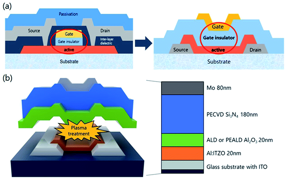 | ||
| Fig. 1 (a) Schematic diagram of self-aligned structured TFT and top-gate bottom-contact structured TFT which have same stack sequence of active/GI/gate and (b) structure of high mobility TFT with the different condition of GI deposition process. | ||
Results and discussions
The transfer characteristics of the top-gate bottom-contact TFTs with various types of GI deposition were investigated. Fig. 2(a) and (b) show the transfer characteristics of each TFT before and after thermal annealing under vacuum conditions, respectively (the overlapped transfer curves of six points for each sample, after thermal annealing, are shown in Fig. S1 in the ESI†). The applied Vd was 0.1 V and the TFTs were 40 and 20 μm in width and length, respectively. Before the annealing process, the TFTs with GIs processed using thermal or PE-ALD, without any plasma treatment, exhibited conductive characteristics. However, on/off characteristics were exhibited when the GI was processed using ALD with O2 or N2O plasma treatment. Both O2 and N2O plasma-treated TFTs exhibited hysteresis, and the O2 plasma-treated sample exhibited a larger hysteresis value, of 14.5 V. Thermal annealing dramatically changed the characteristics of some of the TFTs. The TFT with GI processed by T-ALD without plasma treatment exhibited increased conductivity, whereas desirable TFT characteristics were obtained from the rest of the TFTs, as shown in Fig. 2(b). Furthermore, hysteresis was completely removed after thermal annealing, in the case of the TFT in which the first GI of AlOx was deposited by T-ALD with plasma treatment. Direct deposition of a second GI, of SiNx, on top of the high mobility oxide semiconductor would induce major incorporation of H into the adjacent active layer during post-thermal annealing according to several published paper.30,31 The deposition process would also increase the number of carriers in the oxide semiconductor and degrade the threshold voltage (Vth). However, the ALD-processed thin AlOx, as the first GI, acts as a good H barrier, resulting in devices with reasonable Vth characteristics even in the high mobility TFT.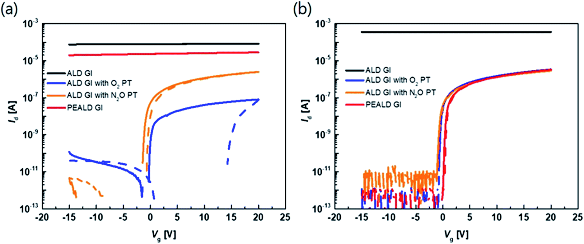 | ||
| Fig. 2 Transfer curve of the TFT with different kinds of GI process with 0.1 V of drain voltage (a) before annealing and (b) after annealing at 300 °C under vacuum. | ||
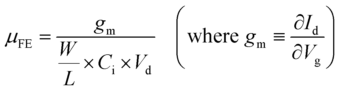
The electrical characteristics, such as field-effect mobility (μFE), subthreshold swing (S.S) and Vth, were evaluated and are listed in Table 1 (a bar graph [with error bars] of the parameters is shown in Fig. S2 in the ESI†). The value of μFE was calculated using the following equation:
| GI process condition | Field-effect mobility (cm2 V−1 s−1) | Subthreshold-swing (V dec−1) | Threshold voltage (V) |
|---|---|---|---|
| ALD GI without PT | NA | NA | NA |
| PEALD GI without PT | 33.2 | 0.10 | 3.06 |
| ALD GI with O2 PT | 35.3 | 0.12 | 2.08 |
| ALD GI with N2O PT | 26.8 | 0.19 | 2.34 |
To investigate the origins of each of the TFT characteristics, we used the Hall measurement method to determine the carrier density of the active layers covered by each GI, which were processed as they would be in the devices. Fig. 3 shows the carrier concentration before and after thermal annealing. Notably, the carrier density of the active layer increased dramatically after thermal annealing when AlOx was deposited using T-ALD without plasma treatment, up to 1.6 × 1020 cm−3; this value is too high to exhibit on/off characteristics. It is well known that a certain amount of H in the channel region acts as a donor by ionizing the H or bonding with oxygen and forming –OH.31,34,35 Therefore, the increase in carrier density after thermal-annealing is caused by H diffusion from the AlOx to the active layer. However, a significant increase in the carrier density of the high-mobility oxide semiconductor was not observed when the plasma treatment was carried out directly before the deposition of AlOx by T-ALD. After the annealing, these samples had similar carrier density, of 1.0 × 1019 cm−3, to that of the active layer covered by PE-ALD processed AlOx. According to Park et al., while the degree of the negative shift in Vth caused by donor incorporation, for example H and O vacancy, may be mild in the case of TFTs with oxide semiconductors of low to moderate carrier density, such as InGaZnO, the doping effect becomes significant when the intrinsic carrier density of the oxide semiconductor is high.36 As shown in Fig. 3, relatively low carrier concentrations were observed when the plasma treatment was performed prior to GI deposition; we observed a mild increase in carrier concentration due to the additional H doping effect. Therefore, TFTs with GIs deposited by T-ALD on active layers treated by O2 and N2O plasma can exhibit reasonable on/off characteristics.
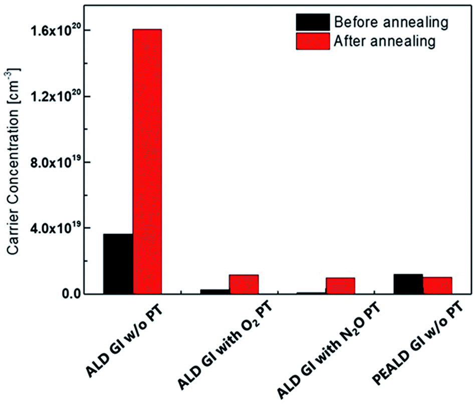 | ||
| Fig. 3 The carrier concentration of the active layer with each GI before and after thermal-annealing. | ||
XPS analysis was carried out to investigate the effects of plasma treatment on the active surface composition and bonding states. We scrutinized the O 1s peaks because the electrical characteristics of oxide semiconductors are strongly related to their oxygen bonding states. The O 1s peaks near 530 eV were measured and de-convoluted with M–O, O vacancies and –OC or –OH bonding, as shown in Fig. 4. It is well known that the binding energies of O vacancies, and –OC and –OH bonds, are relatively large compared to M–O bonds.37–39 From the graph, we can easily see that the amounts of O vacancies, and –OC and –OH bond, decreased dramatically after the plasma treatment. The atomic ratios of the bonding states are summarized in Table 2. The atomic ratio of M–O bonding was approximately 70% before the plasma treatment, increasing to 80% thereafter.
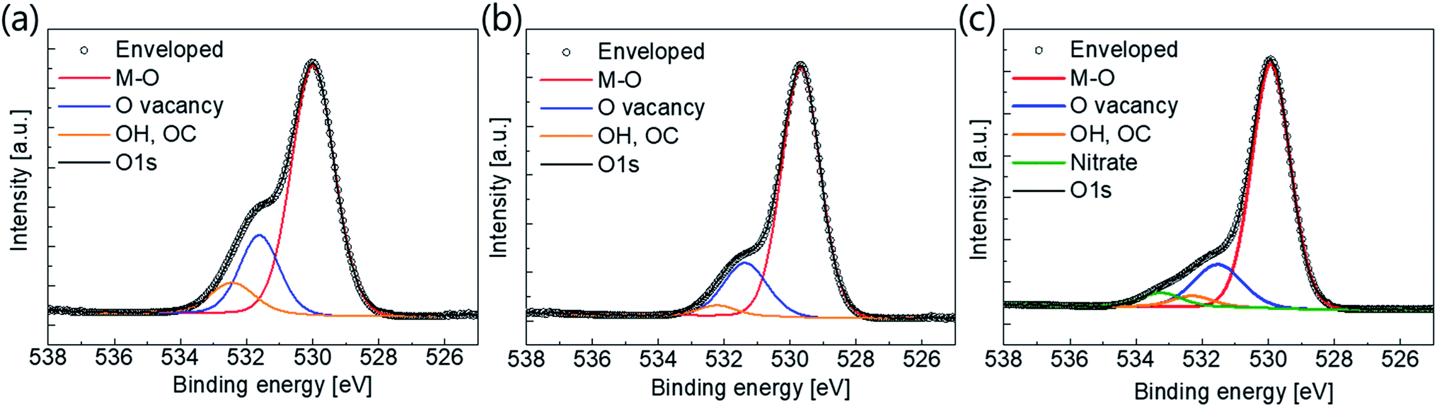 | ||
| Fig. 4 O 1s peaks and de-convoluted peaks from XPS results of (a) pristine active layer, (b) O2 plasma-treated active, and (c) N2O plasma treated active. | ||
| Active state | O–M (at%) | Vo (at%) | OH, OC (at%) | Nitrate (at%) |
|---|---|---|---|---|
| Pristine active | 70.0 | 21.6 | 8.4 | — |
| O2 plasma treated | 80.0 | 16.8 | 3.2 | — |
| N2O plasma treated | 78.7 | 13.4 | 3.2 | 4.7 |
Furthermore, the atomic ratio of O vacancy decreased from 21.6% to 16.8 or 13.4%, depending on the plasma source. The degree of –OC and –OH bonding also decreased. It is well known that O vacancy acts as shallow donors. Therefore, oxygen-containing plasma treatment results in suppression of the intrinsic carrier density. These results are in good agreement with the previously described carrier concentration results. Furthermore, a nitrate peak with a binding energy of 533.2 eV was also detected in the active sample with N2O plasma treatment40 (N 1s XPS peaks are also shown in Fig. S4 in the ESI†). Nitrogen incorporation can occur during N2O plasma treatment; this causes a reduction in the n-type conductivity,32,33 resulting in mobility degradation of the TFT.
The effect of O2 or N2O plasma treatment on the electronic structure of the active films was analyzed using a spectroscopic ellipsometer (SE). The imaginary dielectric-function (ε2) versus photon energy spectra of the Al doped ITZO films with and without O2 or N2O plasma treatment was shown in Fig. 5. These spectra were extracted from a two-phase model, which is composed of a Si substrate and Al doped ITZO layer. The ε2 values near the conduction band minimum (CBM) correlated with the electrical characteristics of the devices.41,42 As shown in the graph, it can be easily noticed that the sub-gap state near CBM was reduced in the Al doped ITZO films by O2 and N2O plasma treatment. Therefore, it can be inferred that the O2 and N2O plasma treatment effectively reduced charge trap sites especially oxygen vacancies.43 This result is well matched with the XPS analysis results. Also, the ε2 just below the CBM is related to the carrier concentration.44 Therefore, decreased ε2 near the CBM after O2 and N2O plasma treatment indicates the reduction of the free carrier concentration of the Al doped ITZO film after O2 and N2O plasma treatment which is correlated with Hall measurement results in Fig. 3. From the SE results, it can be referred that O2 and N2O plasma treatment reduce the oxygen vacancies in the oxide semiconductor effectively to yield improved transfer characteristics as shown in Fig. 2.
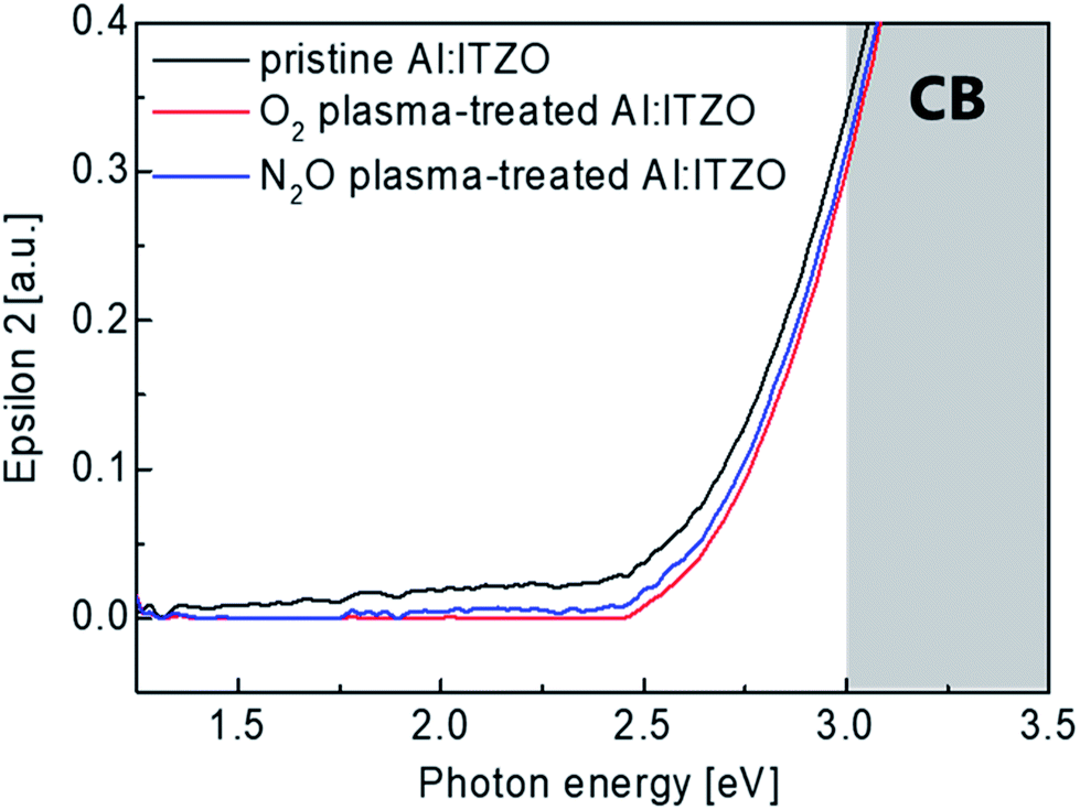 | ||
| Fig. 5 Imaginary dielectric function (ε2) spectra of the Al doped ITZO films with and without O2 or N2O plasma treatment. | ||
The depth profile of the H of a film with the same stack sequence as a fabricated top-gate bottom-contact device was investigated using SIMS measurements. Fig. 6 shows the depth profiles of H after thermal annealing. The H composition varied significantly between the samples. As expected, the larger amount of H was detected in GI with T-ALD than PE-ALD due to H2O reactant. H inside oxide semiconductors acts as a shallow donor to increase the carrier concentration.31,34,35 The film stack sample deposited using T-ALD without plasma treatment contained the largest amount of H in channel region, which explains why the device exhibited conductive characteristics. In contrast, when the plasma treatment was performed prior to the T-ALD process, we observed a reduced amount of H in the channel region. This difference of H amount in channel region can be explained with XPS results which shown in Fig. 4. Many studies have reported that H can introduce to O vacancy sites and act as donor.45,46 As shown in Fig. 4(a), a large amount of O vacancy was observed in the oxide semiconductor without plasma treatment, and a large amount of H can incorporate to the O vacancy sites. On the other hand, in oxide semiconductors with O2 or N2O plasma treatment, the O vacancy decrease significantly, and even oxygen interstitial (Oi) may generated, which plays the role of a charge trap center.47 The hysteresis characteristics of the TFTs before annealing and the reduced carrier concentrations of the active layers covered by ALD GI, with O2 and N2O plasma treatment, support this possibility (see Fig. 2(a) and 3). Therefore, it can be said that the plasma treatment effectively reduces the O vacancy sites where H can induce, so that a smaller amount of H is detected in the SIMS results. When the GI was deposited by PE-ALD without plasma treatment, a moderate amount of H is distributed because, O2 plasma is used as the oxygen source, not H2O during PE-ALD process. Therefore, the TFT exhibited good transfer characteristics, similar to the TFTs with GIs deposited by T-ALD directly after plasma treatment. This resulted in also a moderate carrier concentration in the oxide semiconductor covered by PE-ALD processed AlOx.
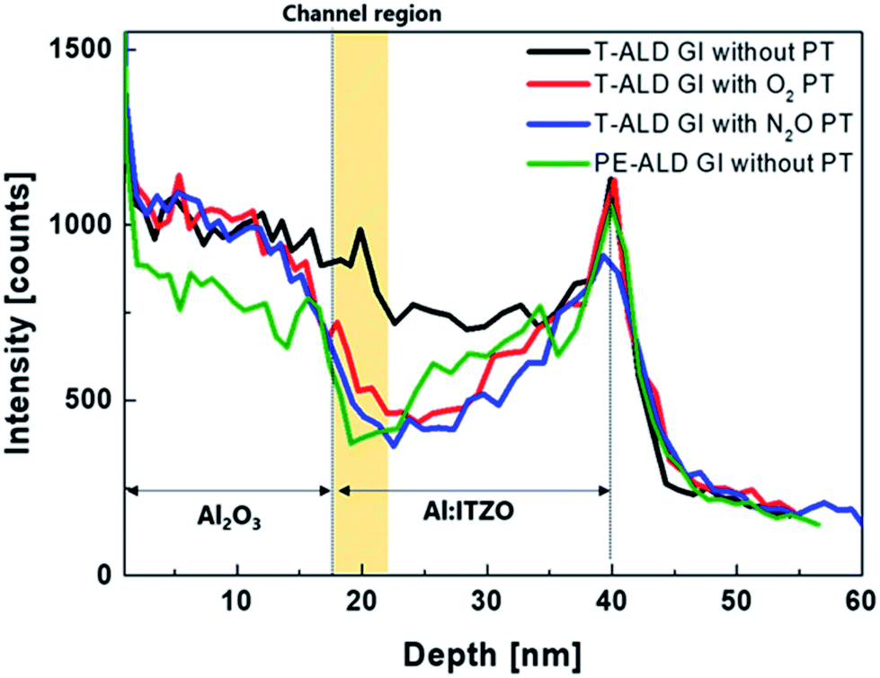 | ||
| Fig. 6 Depth profile of hydrogen element in stacked films with different kinds of GI process after thermal-annealing. | ||
The biggest difference among devices was observed in terms of electrical stability. The transfer curves shown in Fig. 6 were obtained under positive-bias temperature stress (PBTS) conditions. The gate bias and temperature were 20 V (1 MV cm−1) and 60 °C, respectively. The transfer curve shifted significantly in the positive direction when the GI of a given device was deposited using PE-ALD without plasma treatment, as shown in Fig. 7(a). However, when the GI was deposited using T-ALD with plasma treatment, the stability of the device improved significantly. In particular, the device with O2 plasma treatment exhibited outstanding PBTS stability characteristics, shifting by only 0.23 V after 10![[thin space (1/6-em)]](https://www.rsc.org/images/entities/char_2009.gif) 000 s. The transfer curves of the devices with GIs deposited by PE-ALD without plasma treatment, and of GIs deposited by T-ALD with N2O plasma treatment, shifted by 7.49 and 1.23 V, respectively. The variation in Vth during the PBTS is shown in Fig. S5 in the ESI.† The transfer curve of the TFT with GIs processed by PE-ALD shifted significantly during PBTS, without any degradation in the S.S value and no hump generation. This indicates that negative charges are either trapped at the GI and active interface or injected into the GI.24 All of the devices experienced plasma damage during the GI deposition or plasma treatment, and only the plasma-treated devices with GI deposited by T-ALD exhibited high reliability. This was due to defect passivation by H during the T-ALD process and post-thermal annealing. Excessive H renders the oxide TFT conductive, but a moderate amount is beneficial for passivating trap sites at the active and GI interface.24–29 Several cycles of the initial T-ALD AlOx process using a H2O source provide H to passivate the defects generated during O2 or N2O plasma treatment. However, successive incorporation of H can be suppressed by the H barrier constituted by ALD-AlOx itself. The optimized plasma treatment time and T-ALD process temperature can match the degree of defect generation and passivation, which provides excellent electrical performance by minimizing the density of defects at the interface. When PE-ALD is used for GI deposition, the amount of H is insufficient to passivate the defects at the interface,48 so it is difficult to ensure reliability of the device.
000 s. The transfer curves of the devices with GIs deposited by PE-ALD without plasma treatment, and of GIs deposited by T-ALD with N2O plasma treatment, shifted by 7.49 and 1.23 V, respectively. The variation in Vth during the PBTS is shown in Fig. S5 in the ESI.† The transfer curve of the TFT with GIs processed by PE-ALD shifted significantly during PBTS, without any degradation in the S.S value and no hump generation. This indicates that negative charges are either trapped at the GI and active interface or injected into the GI.24 All of the devices experienced plasma damage during the GI deposition or plasma treatment, and only the plasma-treated devices with GI deposited by T-ALD exhibited high reliability. This was due to defect passivation by H during the T-ALD process and post-thermal annealing. Excessive H renders the oxide TFT conductive, but a moderate amount is beneficial for passivating trap sites at the active and GI interface.24–29 Several cycles of the initial T-ALD AlOx process using a H2O source provide H to passivate the defects generated during O2 or N2O plasma treatment. However, successive incorporation of H can be suppressed by the H barrier constituted by ALD-AlOx itself. The optimized plasma treatment time and T-ALD process temperature can match the degree of defect generation and passivation, which provides excellent electrical performance by minimizing the density of defects at the interface. When PE-ALD is used for GI deposition, the amount of H is insufficient to passivate the defects at the interface,48 so it is difficult to ensure reliability of the device.
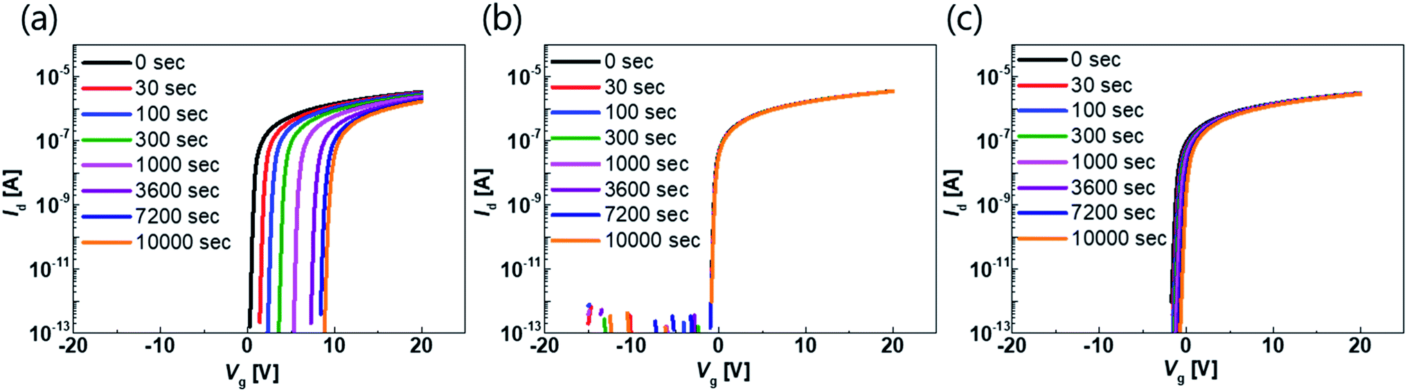 | ||
| Fig. 7 Transfer curve during the PBTS environment of TFT of which alumina first GI was deposited by (a) PEALD without plasma treatment, (b) O2 plasma treatment followed by the thermal-ALD, and (c) with N2O plasma treatment followed by thermal-ALD. | ||
We also investigated the decay in drain current during the on-state bias, where current decay during operation leads to variation in the brightness of current-driven displays, such as OLEDs and LEDs. The normalized change in the amount of drain current was measured under a bias of Vd = 5.5 V and Vg = 5 V, which corresponds to a saturation region. As shown in Fig. 7, the drain current decreases under on-bias due to screening of the gate bias by trapped charges. The on-current decay curves can be fitted with a stretched exponential equation:
 | ||
| Fig. 8 The decay of the normalized drain current during the bias stress and fitted curve with stretched exponential equation. | ||
| GI process condition | τ (s) | β |
|---|---|---|
| PEALD GI without PT | 1.6 × 10⁵ | 0.58 |
| ALD GI with O2 PT | 3.9 × 10¹² | 0.26 |
| ALD GI with N2O PT | 2.7 × 10⁷ | 0.49 |
High-resolution transmission electron microscopy (HRTEM) images of the cross-sections of the active layer/GI stacks in TFTs indicate that the O2 and N2O plasma treatments did not affect the surfaces of the active layers. Fig. 9(a) and (d) show cross-sectional HRTEM images of the channel regions of TFTs with GIs deposited by T-ALD, and by PE-ALD without plasma treatment, respectively. The HRTEM images of the O2 and N2O plasma-treated TFTs are shown in Fig. 9(b) and (c), respectively. There were no significant differences in HRTEM results among the samples. In particular, on scrutinizing the interfaces between the active layers and GIs, the plasma-treated samples contained no crystallized regions, similar to the samples without plasma treatment. It is well known that polycrystalline oxide semiconductors show degraded electrical characteristics, such as low mobility and instability due to grain boundaries.53 The plasma treatment did not provide sufficient energy to allow the active surfaces to crystallize, and there was no change in the phase. Therefore, plasma-treated TFTs maintain their outstanding electrical characteristics.
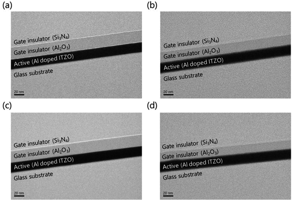 | ||
| Fig. 9 HRTEM images of a cross-section of the channel region in TFT that GI deposited by means of thermal-ALD (a) without plasma treatment, (b) with O2 plasma treatment and (c) N2O plasma-treatment. (d) Is cross-section of the TFT that GI deposited by using PE-ALD without plasma treatment. | ||
Conclusions
High-mobility oxide TFTs with Cu electrodes are promising devices for realizing high-end, large-area displays, such as AMOLEDs and AMLEDs, due to their low RC delay characteristics. SiNx is a suitable candidate for GIs due to its good Cu diffusion barrier and high-k characteristics. To enable use of SiNx as the main GI, we applied a thin AlOx layer as the first GI, which prevents incorporation of H during the SiNx deposition process, as well as the diffusion of H into the active layer during post-thermal annealing. To obtain good stability characteristics, T-ALD was used to deposit AlOx as the first GI. This process does not generate a reactive oxygen plasma source, thus suppressing the generation of charge trapping centers at the interface. To tailor the amounts of shallow H donors and ‘carrier-killer defects’ of interstitial oxygen in the active layer and/or interface, we used O2 or N2O plasma treatment to yield TFTs with improved on/off characteristics. The TFTs subjected to O2 and N2O plasma treatment had Vth values of 2.08 and 2.34 V, respectively. According to our XPS and SIMS results, both O2 and N2O plasma treatment increased the amount of M–O bonding, and reduced the amount of donor elements caused by incorporation of H. The TFT with PE-ALD GIs also exhibited good on/off characteristics, even without any plasma treatment. The Vth of the TFT was approximately 3.06 V. The O2 plasma-treated TFTs with T-ALD GIs exhibited high μFE (>35.3 cm2 V−1 s−1). Furthermore, the TFTs with T-ALD GIs treated by O-containing plasma exhibited improved bias stability compared to the TFT in which AlOx, the first GI, was deposited using PE-ALD. Therefore, we conclude that the T-ALD process for thin GI deposition can be applied to fabricate high-mobility top-gate structured oxide TFTs using O2 or N2O plasma treatment. The AlOx deposited by T-ALD contains appropriate amounts of H, varying by the deposition temperature, and can passivate the extra trap sites generated during oxygen supply for the carrier control process of high-mobility oxide TFTs. Thus, high-mobility, high-stability TFTs can be obtained.Conflicts of interest
There are no conflicts to declare.Acknowledgements
This work was supported by Samsung Display Corporation through KAIST Samsung Display Research Center Program. Also, this work was supported by Wearable Platform Materials Technology Center (WMC) funded by the National Research Foundation of Korea (KRF) Grant by the Korean Government (MSIT) (No. 2016R1A5A1009926).References
- J. Y. Kwon, K. S. Son, J. S. Jung, T. S. Kim, M. K. Ryu, K. B. Park, B. W. Yoo, J. W. Kim, Y. G. Lee, K. C. Park, S. Y. Lee and J. M. Kim, IEEE Electron Device Lett., 2008, 29, 9–302 Search PubMed.
- T. Kamiya, K. Nomura and H. Hosono, Sci. Technol. Adv. Mater., 2010, 11, 044305 CrossRef.
- J.-Y. Kwon, D.-J. Lee and K.-B. Kim, Electron. Mater. Lett., 2011, 7, 1–11 CrossRef CAS.
- J. S. Park, W.-J. Maeng, H.-S. Kim and J.-S. Park, Thin Solid Films, 2012, 520, 1679–1693 CrossRef CAS.
- H.-H. Hsieh, H.-H. Lu, H. C. Ting, C.-S. Chuang, C.-Y. Chen and Y. Lin, J. Inf. Disp., 2010, 11, 160–164 CrossRef.
- T. Wu, C.-W. Sher, Y. Lin, C.-F. Lee, S. Liang, Y. Lu, S.-W. H. Chen, W. Guo, H.-C. Kuo and Z. Chen, Appl. Sci., 2018, 8, 1–17 Search PubMed.
- J. B. Ko, H. I. Yeom and S.-H. K. Park, IEEE Electron Device Lett., 2016, 37, 39–42 CAS.
- H.-I. Yeom, J. B. Ko, G. Mun and S.-H. K. Park, J. Mater. Chem. C, 2016, 4, 6873–6880 RSC.
- E. Lee, A. Benayad, T. Shin, H. Lee, D.-S. Ko, T. S. Kim, K. S. Son, M. Ryu, S. Jeon and G.-S. Park, Sci. Rep., 2014, 4, 4948 CrossRef CAS.
- S. H. Cho, J. B. Ko, M. K. Ryu, J.-H. Yang, H.-I. Yeom, S. K. Lim, C.-S. Hwang and S.-H. K. Park, IEEE Trans. Electron Devices, 2015, 62, 3653–3657 CAS.
- S. Hu, Z. Fang, H. Ning, R. Tao, X. Liu, Y. Zeng, R. Yao, F. Huang, Z. Li, M. Xu, L. Wang, L. Lan and J. Peng, Materials, 2016, 9, 1–5 Search PubMed.
- S. H. Lee, D. J. Oh, A. Y. Hwang, D. S. Han, S. Kim, J. K. Jeong and J. W. Park, IEEE Electron Device Lett., 2015, 36, 802–804 CAS.
- M. J. Powell, C. Glasse, P. W. Green, I. D. French and I. J. Stemp, IEEE Electron Device Lett., 2000, 21, 104–106 CAS.
- K. Nomura, H. Ohta, K. Ueda, T. Kamiya, M. Hirano and H. Hosono, Science, 2003, 300, 1269–1272 CrossRef CAS.
- H. Yabuta, M. Sano, K. Abe, T. Aiba, T. Den, H. Kumomi, K. Nomura, T. Kamiya and H. Hosono, Appl. Phys. Lett., 2006, 89, 112123 CrossRef.
- S.-H. K. Park, C.-S. Hwang, H. Y. Jeong, H. Y. Chu and K. I. Cho, Electrochem. Solid-State Lett., 2008, 11, H10–H14 CrossRef CAS.
- J.-S. Park, J. K. Jeong, Y.-G. Mo and S. Kim, Appl. Phys. Lett., 2009, 94, 042105 CrossRef.
- Y. Kim, K.-H. Lee, G. Mun, K. Park and S.-H. K. Park, Phys. Status Solidi A, 2017, 1700183 CrossRef.
- H. Miyazaki, H. Kojima and K. Hinode, J. Appl. Phys., 1997, 12, 7746–7750 CrossRef.
- G. Dingemans, F. Einsele, W. Beyer, M. C. M. van de Sanden and W. M. M. Kessels, Materials, 2012, 111, 093713 CrossRef.
- L.-L. Zheng, S.-B. Qian, Y.-H. Wang and W.-J. Liu, IEEE J. Electron Devices Soc., 2016, 4, 347–352 CAS.
- J. B. Kim, C. Fuentes-Hernandez, W. J. Potscavage, X.-H. Zhang and B. Kippelen, Appl. Phys. Lett., 2009, 94, 142107 CrossRef.
- M. S. Oh, K. Lee, J. H. Song, B. H. Lee, M. M. Sung, D. K. Hwang and S. Im, J. Electrochem. Soc., 2008, 155, H1009–H1014 CrossRef CAS.
- Y. Nam, H.-O. Kim, S. H. Cho and S.-H. K. Park, RSC Adv., 2018, 8, 5622–5628 RSC.
- K. Nomura, T. Kamiya and H. Hosono, ECS J. Solid State Sci. Technol., 2013, 2, P5–P8 CrossRef CAS.
- Y. Nam, H.-O. Kim, S. H. Cho, C.-S. Hwang, T. Kim, S. Jeon and S.-H. K. Park, J. Inf. Disp., 2016, 17, 65–71 CrossRef CAS.
- Y. Hanyu, K. Domen, K. Nomura, H. Hiramatsu, H. Kumomi, H. Hosono and T. Kamiya, Appl. Phys. Lett., 2013, 103, 202114 CrossRef.
- T. Kim, Y. Nam, J.-H. Hur, S.-H. K. Park and S. Jeon, Nanotechnology, 2016, 27, 325203 CrossRef.
- T. Kamiya and H. Hosono, ECS Trans., 2013, 54, 103–113 CrossRef.
- J.-M. Lee, I.-T. Cho, J.-H. Lee, W.-S. Cheong, C.-S. Hwang and H.-I. Kwon, Appl. Phys. Lett., 2009, 94, 222112 CrossRef.
- K.-L. Han, K.-C. Ok, H.-S. Cho, S. Oh and J.-S. Park, Appl. Phys. Lett., 2017, 111, 063502 CrossRef.
- S. J. Lim, J.-M. Kim, D. Kim, S. Kwon, J.-S. Park and H. Kim, J. Electrochem. Soc., 2010, 157, H214–H218 CrossRef CAS.
- B.-J. Kim, H.-J. Kim, S. M. Jung, T.-S. Yoon, Y.-S. Kim and H. H. Lee, ECS Trans., 2010, 33, 295–299 CAS.
- C. G. Van De Walle, Phys. Rev. Lett., 2000, 85, 1012–1015 CrossRef CAS.
- H. J. Kim, S. Y. Park, H. Y. Jung, B. G. Son, C.-K. Lee, C.-K. Lee, J. H. Jeong, Y.-G. Mo, K. S. Son, M. K. Ryu, S. Lee and J. K. Jeong, J. Phys. D: Appl. Phys., 2013, 46, 055104 CrossRef.
- S.-H. K. Park, M.-K. Ryu, H. Oh, C.-S. Hwang, J.-H. Jeon and S.-M. Yoon, J. Vac. Sci. Technol., B: Nanotechnol. Microelectron.: Mater., Process., Meas., Phenom., 2013, 31, 020601 Search PubMed.
- D.-G. Kim, S. Lee, D.-H. Kim, G.-H. Lee and M. Isshiki, Thin Solid Films, 2008, 516, 2045–2049 CrossRef CAS.
- H. Henriquez, E. Munoz, E. A. Dalchiele, R. E. Marotti, F. Martin, D. Leinen, J. R. Ramos-Barrado and H. Gomez, Phys. Status Solidi A, 2013, 210, 297–305 CrossRef.
- P. K. Nayak, M. N. Hedhili, D. Cha and H. N. Alshareef, Appl. Phys. Lett., 2013, 103, 033518 CrossRef.
- J. F. Moulder, W. F. Stickle, P. E. Sobol and K. D. Bomben, Handbook of X-ray Photoelectron Spectroscopy, ed. J. Chastain, Perkin-Elmer Corporation Physical Electronics Division: Eden Prairie, MN, 1992, ch. II, p. 45 Search PubMed.
- D.-G. Kim, J.-U. Kim, J.-S. Lee, K.-S. Park, Y.-G. Chang, M.-H. Kim and D.-K. Choi, RSC Adv., 2019, 9, 20865–20870 RSC.
- B. D. Ahn, K.-B. Chung and J.-S. Park, J. Electroceram., 2015, 34, 229–235 CrossRef CAS.
- A. Song, H.-W. Park, K.-B. Chung, Y. S. Rim, K. S. Son, J. H. Lim and H. Y. Chu, Appl. Phys. Lett., 2017, 111, 243507 CrossRef.
- S. Yoon, Y. J. Tak, D. H. Yoon, U. H. Choi, J.-S. Park, B. D. Ahn and H. J. Kim, ACS Appl. Mater. Interfaces, 2014, 6, 13496–13501 CrossRef CAS.
- H.-K. Noh, J.-S. Park and K. J. Chang, J. Appl. Phys., 2013, 113, 063712 CrossRef.
- Y. C. Park, J. G. Um, M. Mativenga and J. Jang, ECS J. Solid State Sci. Technol., 2015, 4, Q124–Q129 CrossRef CAS.
- J. Sheng, J. Park, D. W. Choi, J. Lim and J.-S. Park, ACS Appl. Mater. Interfaces, 2016, 8, 31136–31143 CrossRef CAS.
- D.-H. Cho, S.-H. K. Park, S. Yang, C. Byun, K. I. Cho, M. Ryu, S. M. Chung, W.-S. Cheong, S. M. Yoon and C.-S. Hwang, J. Inf. Disp., 2009, 10, 137–142 CrossRef.
- S. Singh and Y. N. Mohapatra, Org. Electron., 2017, 51, 128–136 CrossRef CAS.
- W. H. Lee, S. J. Lee, J. A. Lim and J. H. Cho, RSC Adv., 2015, 5, 78655–78659 RSC.
- J.-M. Lee, I.-T. Cho, J.-H. Lee and H.-I. Kwon, Appl. Phys. Lett., 2008, 93, 093504 CrossRef.
- X.-H. Zhang, S. P. Tiwari and B. Kippelen, Org. Electron., 2009, 10, 1133–1140 CrossRef CAS.
- T. Kamiya, K. Nomura and H. Hosono, Sci. Technol. Adv. Mater., 2010, 11, 1–23 Search PubMed.
Footnote |
| † Electronic supplementary information (ESI) available: The overlapped transfer curve of 6 points of each samples after thermal annealing (Fig. S1), bar graph and error bar of the electrical parameters of the each TFTs (Fig. S2), output curves of the devices (Fig. S3), N 1s peaks of XPS of the active surfaces in each treatment conditions (Fig. S4) and the change of Vth during the PBTS (Fig. S5). See DOI: 10.1039/c9ra06960g |
| This journal is © The Royal Society of Chemistry 2019 |