
 Open Access Article
 This Open Access Article is licensed under a Creative Commons Attribution-Non Commercial 3.0 Unported Licence
Super absorption of solar energy using a plasmonic nanoparticle based CdTe solar cell
Qandeel Rehman†
a,
Aimal Daud Khan†b,
Adnan Daud Khan *a,
Muhammad Nomana,
Haider Alic,
Abdul Raufd and
Muhammad Shakeel Ahmada
*a,
Muhammad Nomana,
Haider Alic,
Abdul Raufd and
Muhammad Shakeel Ahmada
aCenter for Advanced Studies in Energy, University of Engineering & Technology, Peshawar, 25000, Pakistan. E-mail: adnan.daud@uetpeshawar.edu.pk
bCollege of Energy, Soochow Institute for Energy and Materials InnovationS (SIEMIS), Soochow University, Suzhou, 215006, China
cDepartment of Electrical & Electronics Engineering Technology, University of Technology, Nowshera, 24100, Pakistan
dDepartment of Electrical Engineering, National University of Sciences and Technology (NUST), Islamabad, 46000, Pakistan
First published on 23rd October 2019
Abstract
Improving the photon absorption in thin-film solar cells with plasmonic nanoparticles is essential for the realization of extremely efficient cells with substantial cost reduction. Here, a comprehensive study of solar energy enhancement in a cadmium telluride (CdTe) thin-film solar cell based on the simple design of a square array of plasmonic titanium nanoparticles, has been reported. The excitation of localized plasmons in the metallic nanostructures together with the antireflection coating (ARC) significantly enhances the absorption of photons in the active CdTe layer. The proposed structure attained super absorption with a mean absorbance of more than 97.27% covering a wide range from visible to near-infrared (i.e., from 300 nm to 1200 nm), presenting a 90% absorption bandwidth over 900 nm, and the peak absorption is up to 99.9%. For qualitative analysis, the photocurrent density is also estimated for AM 1.5 solar illumination (global tilt), whose value reaches 40.36 mA cm−2, indicating the highest value reported to date. The impact of nanoparticle dimensions, various metal materials, shapes, and random arrangement of nanoparticles on optical absorption are discussed in detail. Moreover, the angle insensitivity is essentially validated by examining the absorption performance with oblique incidences and it is found that the solar cell keeps high absorption efficiency even when the incidence angle is greater than 0°. Therefore, these findings suggest that the proposed broadband structure has good prospect in attaining high power conversion efficiency while reducing the device cost.
Introduction
Thin film solar cells are being researched extensively worldwide due to their flexible structure, lower weight, simple fabrication and integration procedures. These solar cells, despite having many advantages, have a drawback of lower optical conversion efficiency compared to its conventional counterpart i.e. c-Si solar cells. The lower efficiency is mainly due to small thickness (1–2 μm), where most of the low frequency photons escape from the cell.1 A number of techniques have been proposed to trap the light inside the solar cell, which include photonic crystals,2 diffraction gratings,3 anti-reflection coating (ARC),4 and metallic nanoparticles.5,6 These methods are used to reduce the reflection of incoming light at the front surface and minimize the transmission of light at the rear surface of the solar cell. Among these techniques, the plasmonic nanoparticle approach is considered to be the best one as it utilizes surface plasmons to enhance the absorption in the active layer of the solar cell.7–9Recently, it has been found that cadmium telluride (CdTe) is the most promising candidate for the active layer among thin-film solar cells due to its long-term stability and capability of photon absorption in visible and near infrared region.10 Furthermore, it is a direct bandgap semiconductor with optical absorption coefficient of 105 cm−1 and they are also commercially available.11,12 When the nanoparticles are deposited on CdTe based solar cell, the absorption efficiency is improved in greater amount. Y. Shao et al.,13 proposed an efficient structure for capturing light in CdTe solar cells. The transmission of incoming light is maximized at the front surface by 73% in the wavelength range 300–900 nm by depositing an array of gold nanoparticles on the back surface of the absorber layer. D. Liu et al.,14 proposed a novel design for light management in CdTe solar cells, where an array of spherical silver nanoparticles was deposited at the bottom surface of the absorbing layer to achieve 50% absorption rate. The efficiency increase was observed for light spectrum in wavelength range 300–500 nm. A. Araujo et al.,15 worked on increasing light trapping in thin film solar cells by depositing silver nanoparticles at rear surface of cells thus increasing the absorption up to 90% in light spectrum ranging 450–700 nm. Q. Luo et al.,7 proposed the integration of gold on TiO2 nanospheres in porous layers of TiO2 as well as perovskite to increase the power conversion efficiency to 18.24% thus making an improvement of 44% over the reference model. The absorption efficiency was measured for this model in the wavelength ranging from 300 to 800 nm. N. Spalatu et al.,16 achieved 75% absorption efficiency by deposition of gold nanoparticles on front surface of CdTe solar cells for efficiency enhancement in the wavelength ranging from 500 nm to 850 nm.
In this paper, a simple CdTe solar cell is proposed, which consists of cuboid titanium (Ti) nanoparticles on top of SiO2 ARC. Broadband absorption efficiency is achieved in the solar spectrum with an average absorption of more than 97.27%. The absorption resonance is improved by optimizing different layers of the solar cell structure. Oblique incidences are also examined to demonstrate the angle insensitivity of the solar cell.
Model
The schematic of the proposed structure is shown in Fig. 1, which is made up of five different layers. The absorbing layer is made of cadmium telluride (CdTe) material, which has high absorption coefficient of 105 cm−1 and bandgap of 1.5 eV. This material is also known for its cost effectiveness in terms of manufacturing and fabrication process.17 Indium tin oxide (ITO) material is chosen as transparent conductive oxide (TCO) for the back surface, which increases light trapping by providing resistance for low energy photons at back surface, thus reflecting long wavelength light (600–1200 nm), and reducing transmission losses significantly in solar cells.18 The cell is coated with an anti-reflection coating (ARC) made of SiO2 to reduce reflection losses on the front surface.19 The ARC is further coated with cubic plasmonic titanium (Ti) nanoparticles and is protected with a glass layer made of quartz. Nanoparticles increase energy of incident photons and scatter it into substrate that has high refractive index.20 The reason of choosing Ti material is that, it has high transmittance in visible and ultra-violet light ranges in solar radiation spectrum and is highly resistive to corrosion. The quartz glass layer is highly resistive to thermal losses and has high transmittance in ultraviolet to near-infrared light ranges.21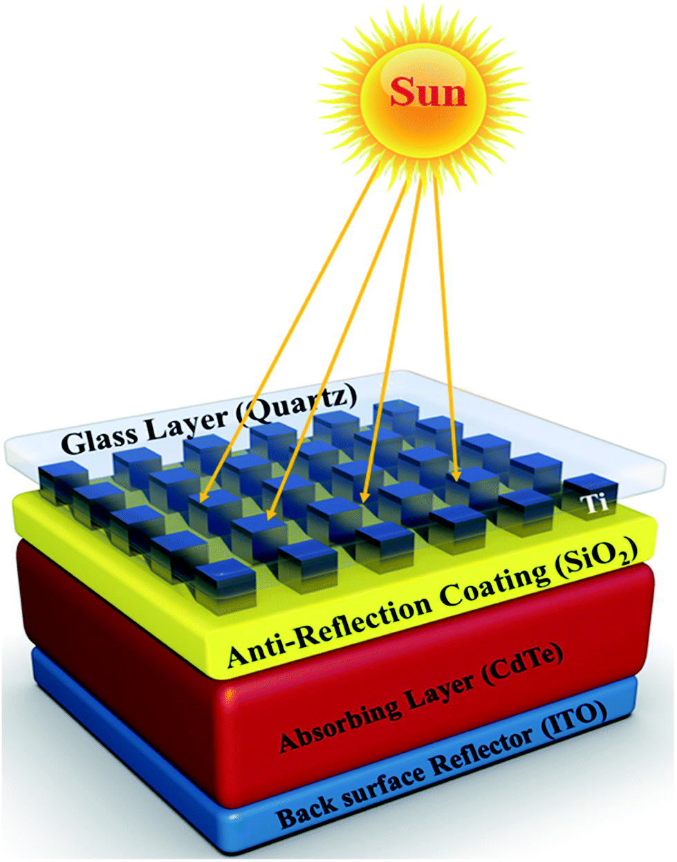 | ||
| Fig. 1 Geometric sketch of the super broadband solar energy absorber. | ||
The optimized model shown in Fig. 2(a) and (b) consists of cuboid nanoparticles with dimensions (Sn × tn × Sn) 90 × 90 × 50 nm3 and a total volume of 405![[thin space (1/6-em)]](https://www.rsc.org/images/entities/char_2009.gif) 000 nm3. The particles are placed at a distance of gn = 120 nm from consecutive nanoparticles, which will enhance the absorption efficiency due to coupling and interaction of surface plasmons. A unit cell of (lx × ly) 400 × 400 = 1600 nm2 having four Ti nanoparticles and the cell structure shown in Fig. 2(b), is simulated in the RF module of Comsol Multiphysics software. Two sides of the unit cell, which are in the direction of the incident field polarization, are made from perfect electric conductor (PEC), and the remaining two sides are made from perfect magnetic conductor (PMC). The solar cell is illuminated by light in the z-direction, while polarization is set along x-axis. A perfectly matched layer (PML) is also placed at the top and bottom of the unit cell, whose job is to eliminate the back reflections from the boundaries. The Floquet periodic boundary conditions are used for repetition of unit cell in both x and y-directions. The thicknesses of quartz glass, nanoparticles, ARC, absorber and ITO back surface reflector are denoted by tglass, tn, tarc, tabs and tbsf, respectively. The complex dielectric functions of CdTe, SiO2, Ti, and ITO are taken from.22 The environment of the simulation is selected as air and for further analysis, Matlab software is used.
000 nm3. The particles are placed at a distance of gn = 120 nm from consecutive nanoparticles, which will enhance the absorption efficiency due to coupling and interaction of surface plasmons. A unit cell of (lx × ly) 400 × 400 = 1600 nm2 having four Ti nanoparticles and the cell structure shown in Fig. 2(b), is simulated in the RF module of Comsol Multiphysics software. Two sides of the unit cell, which are in the direction of the incident field polarization, are made from perfect electric conductor (PEC), and the remaining two sides are made from perfect magnetic conductor (PMC). The solar cell is illuminated by light in the z-direction, while polarization is set along x-axis. A perfectly matched layer (PML) is also placed at the top and bottom of the unit cell, whose job is to eliminate the back reflections from the boundaries. The Floquet periodic boundary conditions are used for repetition of unit cell in both x and y-directions. The thicknesses of quartz glass, nanoparticles, ARC, absorber and ITO back surface reflector are denoted by tglass, tn, tarc, tabs and tbsf, respectively. The complex dielectric functions of CdTe, SiO2, Ti, and ITO are taken from.22 The environment of the simulation is selected as air and for further analysis, Matlab software is used.
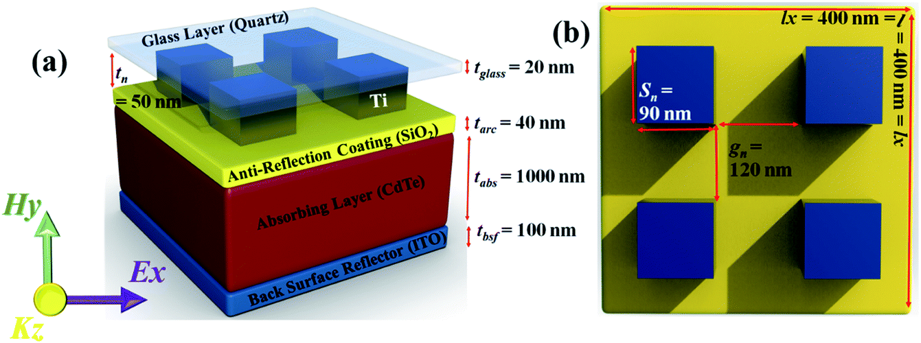 | ||
| Fig. 2 (a) 3D view of the proposed structure in a unit cell, and (b) top view of the structure. | ||
Results and discussion
To investigate the effect of Ti nanoparticles on CdTe solar cell, a 1000 nm CdTe absorber layer with 100 nm ITO as a back surface reflector is taken as a reference cell. The ARC and nanoparticle layers were added to the reference cell to analyze the increase in absorption efficiency as shown in Fig. 3. The reference unit solar cell is named as M1, while other models were named as M2, M3, M4, and M5, presented by Fig. 3(a–e).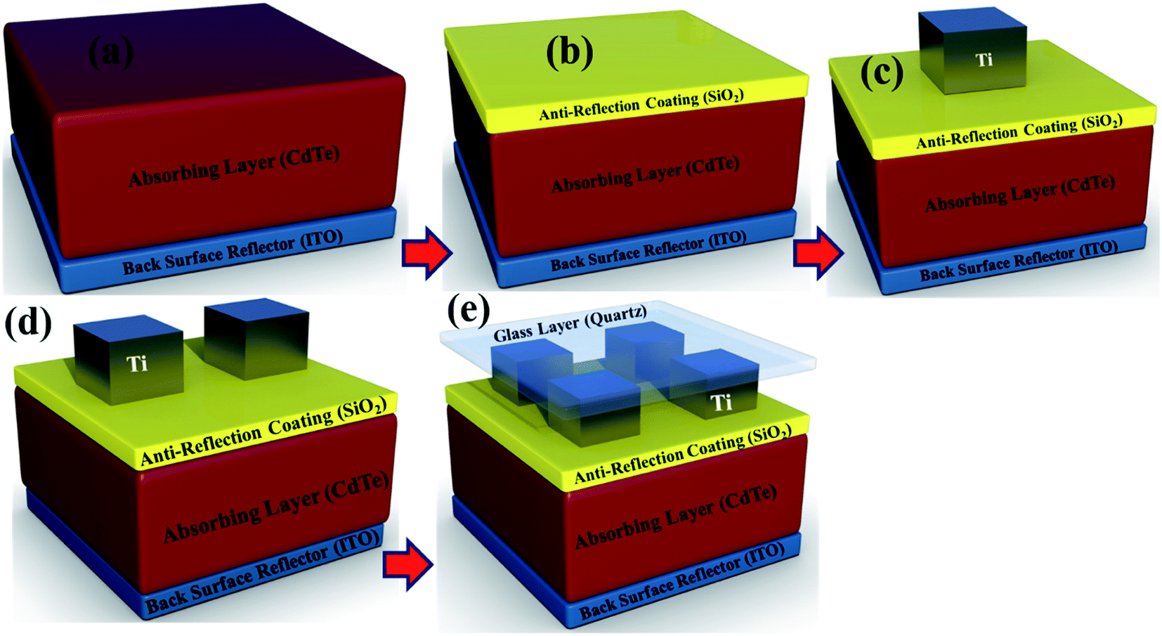 | ||
| Fig. 3 Different designs of CdTe solar cells (a) reference solar cell of CdTe solar cell with ITO (M1), (b) unit cell consisting of M1 with ARC layer (M2), (c) unit cell with addition of 1 nanoparticle (M3), (d) unit cell with two nanoparticles (M4), and (e) unit cell with four nanoparticles and quartz glass on top of nanoparticle layer (M5). | ||
The absorption efficiencies of all the models are displayed in Fig. 4(a). It is found that the reference cell M1 exhibits 60–70% absorption efficiency in 300–500 nm wavelength range, which increases to approximately 83% at 600 nm and 92% at 1120 nm as indicated by the green curve. The slightly high absorption efficiency is due to large absorption coefficient of CdTe material. However, this efficiency is not enough for a generation of electron–hole pairs for solar energy harvesting applications. In other words, absorber layer with back surface reflector shows lesser photon absorption capability if modeled without nanoparticles.23 For minimizing such optical losses, a 40 nm SiO2 ARC layer is added on top of reference model M1 and is labeled Model M2 as shown in Fig. 3(b). The absorption efficiency of M2 is represented by the blue curve in Fig. 4(a), which shows an average increment of approximately 10% in absorption efficiency. In this case, the response is almost flat as no sharp dips are observed in the solar spectrum. The accumulative absorption efficiency of model M2 becomes 70%.
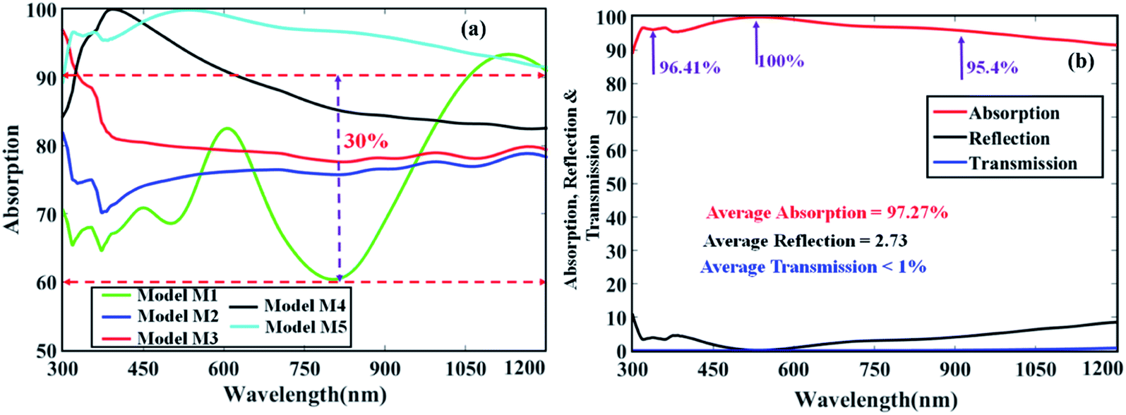 | ||
| Fig. 4 (a) Optical absorption efficiency of models M1–M5, (b) optical absorption, reflection, and transmission of model M5. | ||
The third model M3 is obtained by the deposition of cuboid Ti nanoparticle with dimensions 90 × 90 × 50 nm3 on M2, as shown in Fig. 3(c). Fig. 4(a) shows the absorption efficiency of M3 (red curve), which has a mean value of nearly 80%. The improvement in absorption efficiency is observed due to scattering of light using Ti nanoparticle excited at their surface plasmon resonance. Thus, in comparison to M2, M3 shows increase in absorption efficiency at lower wavelength range, however no significant difference at higher wavelength range is observed.
The model M4 represents iteration of M3, where a second nanoparticle is added 120 nm away from the first nanoparticle on ARC layer, as depicted in Fig. 3(d). The designed model further improves the absorption efficiency due to coupling and interference of plasmonic modes exhibited by the nanoparticles and the modes of ARC, and CdTe layers. In this case, a broad absorption mode with amplitude of near unity at 395 nm is observed as shown in Fig. 4(a). To obtain super broadband absorption efficiency, we added four nanoparticles on top of M2, each at a distance of 120 nm from consecutive nanoparticles as shown in Fig. 3(e). A 20 nm quartz layer is also added in M5 to protect the cell from UV radiations. Here, the surface plasmons of all four nanoparticles strongly interact with each other, which results in a super broadband absorption with mean efficiency of approximately 97% from 300–1200 nm as shown in Fig. 4(a) (sky-blue curve). The optical absorption spectra is improved up to 30% as compared to reference model indicated by difference shown between two dotted lines in Fig. 4(a). Moreover, the corresponding current density (Jsc) is also estimated using eqn (1).24
 | (1) |
From the evaluation of M1–M5 given in Fig. 4, it is observed that the deposition of multiple metallic nanoparticles on the top surface of solar cell increases surface plasmon resonance (SPR) when it is hit by an incident light, which further enhances the absorption efficiency. Since the SPR depends on the material of the nanoparticles,25 therefore, the influence of optical absorption and flexibility of the proposed structure on material selection is investigated as shown in Fig. 5(a). Numerical simulation is executed for different types of materials show that Ti based nanoparticles deposited on solar cell exhibits super broadband optical absorption compared to the rest of the materials. This may be due to destructive interference between incident and scattered radiations in case of Ti is very less compared to other materials.26
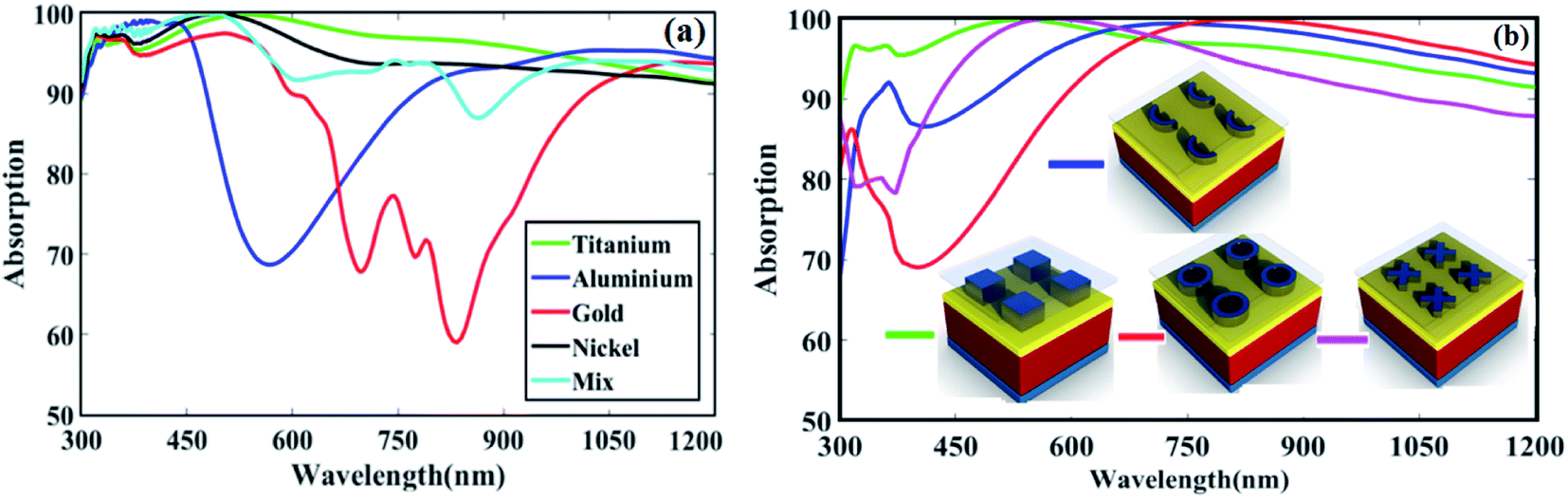 | ||
| Fig. 5 Influence of the optical absorption over (a) different materials, and (b) different shapes of the nanoparticle. | ||
The optical absorption efficiency also changes with the shape of nanoparticles.27 To assess this hypothesis, different geometric configurations of nanoparticles such as cross shape, hollow cylindrical and semi-circular shapes are simulated to evaluate the absorption efficiency. The results are compared with the cuboid nanoparticle model proposed in this study, as depicted in Fig. 5(b). It is found that the proposed model possesses much a better spectral performance than other simulated geometric shapes of nanoparticles. This is because the total volume of the cuboid shape nanoparticles are large due to which it supports strong surface plasmon resonances compared to others, and enhances the absorption efficiency in greater amount.
Since, the Ti cuboid nanoparticles deposited on solar cell are found to be a best choice, therefore, to further optimize the design for maximizing efficiency, the dimensions of the nanoparticle is varied and keeping other parameters constant. It is has been observed in Fig. 6(a) that, as the thickness tn of nanoparticles increases from 10–50 nm, the optical absorption efficiency increases in visible as well as in near-infrared region of the solar spectrum. This is because for small nanoparticles, the excited SPR's energy generally lost within the nanoparticle and the scattering becomes insignificant, hence no improvement in absorption efficiency can be seen. However, for any thickness value more than 50 nm, the nanoparticles show a descending trend in photon absorption over shorter wavelengths, thus decreasing the overall efficiency. This is due to the fact that for large nanoparticles, the scattering overcomes the lossy absorption. So, the forward scattering becomes predominant and mostly prevails at frequencies lower than the SPR, thus letting more photon energy to enter into the absorber layer, which ultimately leads to improved absorption efficiency over the whole solar spectrum. Moreover, large nanoparticles support higher order plasmonic modes, which also contribute in the absorption characteristics of the solar cell. However, as the size exceeds 50 nm, which in our case is the optimal value, the absorption efficiency reduces because the backward scattering overcomes the forward scattering due to the incoming light shielding engendered by the huge surface charge density of Ti nanoparticles. In addition, for large nanoparticles, the mismatch between the scattering light and the incident field also increases, which restructures the entire absorption spectrum, particularly for wavelengths larger than the SPR. Therefore, choosing proper size of the nanoparticles, the incoming photons can be efficiently coupled into the absorber layer with the absorption optimally matched with the solar spectrum.
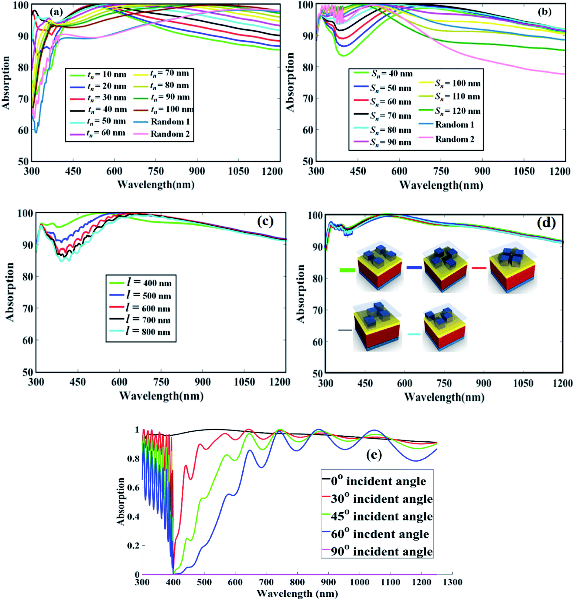 | ||
| Fig. 6 Influence of optical absorption spectra over (a) thickness of the nanoparticles, (b) size of the nanoparticles, (c) different periods, (d) different arrangement of nanoparticles, and (e) different incidence angles. | ||
Since experimentally, it is very challenging to fabricate all dimensions of the nanoparticles same as modeled theoretically, therefore, two random thicknesses of cubic Ti nanoparticles are simulated to cover the possibility of variation in the software defined thickness. Both tests exhibit approximately same performance as indicated by curves ‘Random 1’ and ‘Random 2’ in Fig. 6(a).
The size Sn effect on absorption efficiency is more or less the same as tn as shown in Fig. 6(b). It is evident that as the size of the nanoparticles increases from 40–90 nm, surface plasmon excitation increases, which boost the optical absorption efficiency. At 90 nm, maximum interaction of surface plasmons is observed with each other due to which the light absorption is improved. However, if the size is further increased from 90–120 nm, the efficiency decreases especially at longer wavelengths i.e., from 600–1200 nm. This is again because, the phase mismatch between the incident and the scattering light increases for large nanoparticles. Two random tests are also performed in this case, where still higher absorption efficiency is achieved, which indicates that the proposed design is highly suitable for practical applications.
In Fig. 6(c), the influence of varying dimensions of unit cell on optical absorption efficiency is measured over the wavelength range of 300–1200 nm while keeping all the other parameters fixed. The results show that as the size of the period increases, the absorption spectra at short wavelength gradually decreases. This is due to increase of gap between two unit cells which causes reduction in coupling strength of surface plasmons between two unit cells. Since, coupling strength boosts the intensity of the incoming photons, its reduction causes absorption spectra losses at shorter wavelengths.28 Furthermore, we performed another test by depositing the nanoparticles randomly as shown in Fig. 6(d). It is observed that the random arrangement does not affect the absorption profile of the solar cell, which proves that the proposed structure is polarization independent.
Eventually, the absorption characteristics of the proposed structure is tested for different incident angles of light, as shown in Fig. 6(e). At 0° angle, i.e., when the direction of propagation of light is perpendicular to the plan of CdTe solar cell surface, maximum absorption efficiency is observed. This absorption efficiency decreases with increase in angle of incidence and becomes almost equal to 0 at 90° when the direction of propagation of wave is parallel to the surface of solar cell. However, for angles greater than 0°, the absorption profile is still acceptable as its average value for longer wavelengths is approximately 80%. This indicates that the CdTe solar cell presented in this study is highly suitable for practical applications.
The performance of the proposed CdTe solar cell structure is compared with other plasmonic nanoparticle based solar cells. The shapes of different nanoparticles along with the spectrum of light and bandwidth and the percentage absorption efficiency in that bandwidth region is presented in Table 1. The results indicate that our suggested structure has greatest absorption peak and covers broadband spectrum whereas other nanoparticles cover specific regions in the solar spectrum. This indicates that proposed design is much better than the previously reported light trapping techniques for solar cells using plasmonic effect.
| Shapes | Materials | Light spectrum (nm) | Bandwidths (nm) | Optical absorption rate (%) | Solar cell material | Ref. |
|---|---|---|---|---|---|---|
| Square | Aluminum on top of polymethylmethacrylate (PMMA) | 425–650 | 300 | 90 | Si | 29 |
| Triangular prism and nanosphere | Silver | 300–700 | 400 | 90 | a-Si | 30 |
| Ring | Chromium | 500–800 | 300 | 95 | N/A | 31 |
| Circular nanocavity | Silver | 750–1000 | 250 | 60 | c-Si TFSC | 32 |
| Cuboid | Ti | 300–1200 | 900 | 98.98 | CdTe | Proposed design |
Conclusion
We have suggested a new thin-film CdTe solar cell, which is based on comparatively cost-effective Ti nanoparticles. The proposed structure exhibits almost unity absorption with a mean absorption of 97.27% and 90% absorption bandwidth over 900 nm from visible to near-infrared region. The broadband response and the high absorption typically result from the strong electromagnetic resonance and overlapping of resonant frequencies. The structure exhibit Jsc of 40.36 mA cm−2, which is the highest value reported up to date. The effects of nanoparticle dimensions, different metal materials, shapes and different random locations on the absorption patterns are compared to analyze the characteristics of the proposed solar cell. Moreover, it is found that solar cell possesses high absorption efficiency even when the incidence angle is more than 0°. Despite the relatively simple structure, such a design exhibits high performance in both the bandwidth and absorptivity and can be easily extended to other thin solar cell technologies.Conflicts of interest
There are no conflicts to declare.References
- J. Poortmans and V. Arkhipov, Thin film solar cells: fabrication, characterization and applications, John Wiley & Sons, 2006, vol. 5 Search PubMed.
- W. Zhang, M. Anaya, G. Lozano, M. E. Calvo, M. B. Johnston and H. n. Míguez, et al., Highly efficient perovskite solar cells with tunable structural color, Nano Lett., 2015, 15, 1698–1702 CrossRef CAS.
- R. Dewan and D. Knipp, Light trapping in thin-film silicon solar cells with integrated diffraction grating, J. Appl. Phys., 2009, 106, 074901 CrossRef.
- A. Rahman, A. Ashraf, H. Xin, X. Tong, P. Sutter and M. D. Eisaman, et al., Sub-50-nm self-assembled nanotextures for enhanced broadband antireflection in silicon solar cells, Nat. Commun., 2015, 6, 5963 CrossRef CAS.
- A. D. Khan, A. D. Khan, S. D. Khan and M. Noman, Light absorption enhancement in tri-layered composite metasurface absorber for solar cell applications, Opt. Mater., 2018, 84, 195–198 CrossRef CAS.
- A. D. Khan, J. Iqbal and S. ur Rehman, Polarization-sensitive perfect plasmonic absorber for thin-film solar cell application, Appl. Phys. A: Mater. Sci. Process., 2018, 124, 610 CrossRef.
- Q. Luo, C. Zhang, X. Deng, H. Zhu, Z. Li and Z. Wang, et al., Plasmonic effects of metallic nanoparticles on enhancing performance of perovskite solar cells, ACS Appl. Mater. Interfaces, 2017, 9, 34821–34832 CrossRef CAS.
- R.-H. Fan, L.-H. Zhu, R.-W. Peng, X.-R. Huang, D.-X. Qi and X.-P. Ren, et al., Broadband antireflection and light-trapping enhancement of plasmonic solar cells, Phys. Rev. B: Condens. Matter Mater. Phys., 2013, 87, 195444 CrossRef.
- A. D. Khan, A. D. Khan, F. E. Subhan and M. Noman, Efficient Light Management in Ultrathin Crystalline GaAs Solar Cell Based on Plasmonic Square Nanoring Arrays, Plasmonics, 2019, 1–8 Search PubMed.
- D. Cusano, CdTe solar cells and photovoltaic heterojunctions in II–VI compounds, Solid-State Electron., 1963, 6, 217–232 CrossRef CAS.
- M. Dongol, A. El-Denglawey, M. A. El Sadek and I. Yahia, Thermal annealing effect on the structural and the optical properties of Nano CdTe films, Optik, 2015, 126, 1352–1357 CrossRef CAS.
- N. Strevel, L. Trippel, C. Kotarba and I. Khan, Improvements in CdTe module reliability and long-term degradation through advances in construction and device innovation, Photovoltaics International, 2013, 22, 66–74 Search PubMed.
- Y. Shao, X. Li, L. Wu and D. Wang, Cu diffusion in CdTe detected by nano-metal-plasmonic enhanced resonant Raman scattering, J. Appl. Phys., 2019, 125, 013101 CrossRef.
- D. Liu, J. Chen, D. Wang, L. Wu and D. Wang, Enhanced surface optical phonon in CdTe thin film observed by Raman scattering, Appl. Phys. Lett., 2018, 113, 061604 CrossRef.
- A. Araujo, M. J. Mendes, T. Mateus, J. Costa, D. Nunes and E. Fortunato, et al., Ultra-fast plasmonic back reflectors production for light trapping in thin Si solar cells, Sol. Energy, 2018, 174, 786–792 CrossRef CAS.
- N. Spalatu, J. Hiie, N. Maticiuc, M. Krunks, A. Katerski and V. Mikli, et al., Plasmonic effect of spray-deposited Au nanoparticles on the performance of CSS CdS/CdTe solar cells, Appl. Surf. Sci., 2015, 350, 69–73 CrossRef CAS.
- A. Babayigit, A. Ethirajan, M. Muller and B. Conings, Toxicity of organometal halide perovskite solar cells, Nat. Mater., 2016, 15, 247 CrossRef CAS.
- J. You, L. Meng, T.-B. Song, T.-F. Guo, Y. M. Yang and W.-H. Chang, et al., Improved air stability of perovskite solar cells via solution-processed metal oxide transport layers, Nat. Nanotechnol., 2016, 11, 75 CrossRef CAS.
- M. Mazur, D. Wojcieszak, D. Kaczmarek, J. Domaradzki, S. Song and D. Gibson, et al., Functional photocatalytically active and scratch resistant antireflective coating based on TiO2 and SiO2, Appl. Surf. Sci., 2016, 380, 165–171 CrossRef CAS.
- F. Martinez-Gutierrez, P. L. Olive, A. Banuelos, E. Orrantia, N. Nino and E. M. Sanchez, et al., "Synthesis, characterization, and evaluation of antimicrobial and cytotoxic effect of silver and titanium nanoparticles, Nanomedicine, 2010, 6, 681–688 CrossRef CAS.
- W. S. Rodney and R. J. Spindler, Index of refraction of fused quartz glass for ultraviolet, visible, and infrared wavelengths, J. Opt. Soc. Am., 1954, 44, 677–679 CrossRef CAS.
- X. Ni, Z. Liu, and A. V. Kildishev, Photonics DB: Optical Constants, 2007 Search PubMed.
- E. Shi, H. Li, L. Yang, L. Zhang, Z. Li and P. Li, et al., Colloidal antireflection coating improves graphene–silicon solar cells, Nano Lett., 2013, 13, 1776–1781 CrossRef CAS.
- C. Zhang, D. O. Guney and J. M. Pearce, Plasmonic enhancement of amorphous silicon solar photovoltaic cells with hexagonal silver arrays made with nanosphere lithography, Mater. Res. Express, 2016, 3, 105034 CrossRef.
- B. Dastmalchi, P. Tassin, T. Koschny and C. M. Soukoulis, A new perspective on plasmonics: confinement and propagation length of surface plasmons for different materials and geometries, Adv. Opt. Mater., 2016, 4, 177–184 CrossRef CAS.
- S. Lim, W. Mar, P. Matheu, D. Derkacs and E. Yu, Photocurrent spectroscopy of optical absorption enhancement in silicon photodiodes via scattering from surface plasmon polaritons in gold nanoparticles, J. Appl. Phys., 2007, 101, 104309 CrossRef.
- S. Kumar, A. C. Anselmo, A. Banerjee, M. Zakrewsky and S. Mitragotri, Shape and size-dependent immune response to antigen-carrying nanoparticles, J. Controlled Release, 2015, 220, 141–148 CrossRef CAS.
- S.-Y. Ding, J. Yi, J.-F. Li, B. Ren, D.-Y. Wu and R. Panneerselvam, et al., Nanostructure-based plasmon-enhanced Raman spectroscopy for surface analysis of materials, Nat. Rev. Mater., 2016, 1, 16021 CrossRef CAS.
- R. Mudachathi and T. Tanaka, Broadband plasmonic perfect light absorber in the visible spectrum for solar cell applications, Adv. Nat. Sci.: Nanosci. Nanotechnol., 2018, 9, 015010 Search PubMed.
- W. Ren, G. Zhang, Y. Wu, H. Ding, Q. Shen and K. Zhang, et al., Broadband absorption enhancement achieved by optical layer mediated plasmonic solar cell, Opt. Express, 2011, 19, 26536–26550 CrossRef CAS PubMed.
- I. Kim, S. So, A. S. Rana, M. Q. Mehmood and J. Rho, Thermally robust ring-shaped chromium perfect absorber of visible light, Nanophotonics, 2018, 7, 1827–1833 CAS.
- S. Roy, Circular Nanocavity in Ultrathin c-Si Solar Cell for Efficient Light Absorption, Plasmonics, 2018, 13, 1499–1504 CrossRef.
Footnote |
| † The first two authors contribute equally. |
| This journal is © The Royal Society of Chemistry 2019 |