
 Open Access Article
 This Open Access Article is licensed under a Creative Commons Attribution-Non Commercial 3.0 Unported Licence
Solution based synthesis of Cu(In,Ga)Se2 microcrystals and thin films
M. Latha *a,
R. Aruna-Devia,
S. Velumani*b,
B. Muralic,
J. Santoyo-Salazard and
F. de Moure-Floresa
*a,
R. Aruna-Devia,
S. Velumani*b,
B. Muralic,
J. Santoyo-Salazard and
F. de Moure-Floresa
aFacultad de Química, Materiales-Energía, Universidad Autónomade Querétaro (UAQ), Santiago de Querétaro, Qro C.P.76010, Mexico. E-mail: lathamarasamy@gmail.com
bDepartamento de Ingeniería Eléctrica, CINVESTAV-IPN, Av. IPN 2508, San Pedro Zacatenco, C.P. 07360 Ciudad de México, Mexico. E-mail: velu@cinvestav.mx
cSolar Cells and Photonics Research Laboratory, School of Chemistry, University of Hyderabad, Prof. C. R. Rao Road, Telangana, India 500046
dDepartamento de Física, CINVESTAV-IPN, Av. IPN 2508, San Pedro Zacatenco, C.P. 07360 Ciudad de México, Mexico
First published on 30th October 2019
Abstract
Herein, for the first time, we report the synthesis of quaternary Cu(In,Ga)Se2 microcrystals (CIGSe MCs) using a facile and economical one-pot heating-up method. The most important parameters such as reaction temperature and time were varied to study their influences on the structural, morphological, compositional and optical properties of the MCs. Based on the results, the formation of CIGSe was initiated from binary β-CuSe and then converted into pure phase CIGSe by gradual incorporation of In3+ and Ga3+ ions into the β-CuSe crystal lattice. As the reaction time increases, the band gap energy was increased from 1.10 to 1.28 eV, whereas the size of the crystals increased from 0.9 to 3.1 μm. Besides, large-scale synthesis of CIGSe MCs exhibited a high reaction yield of 90%. Furthermore, the CIGSe MCs dispersed in the ethanol was coated as thin films by a drop casting method, which showed the optimum carrier concentration, high mobility and low resistivity. Moreover, the photoconductivity of the CIGSe MC thin film was enhanced by three order magnitude in comparison with CIGSe NC thin films. The solar cells fabricated with CIGSe MCs showed the PCE of 0.59% which is 14.75 times higher than CIGSe NCs. These preliminary results confirmed the potential of CIGSe MCs as an active absorber layer in low-cost thin film solar cells.
Introduction
Cu(In,Ga)Se2 (CIGSe) has been considered as the most promising absorber material in thin film solar cells due to its direct band gap, high absorption co-efficient (>105 cm−1), tunable band gap from 1 to 1.7 eV, good photo stability and radiation hardness.1–5 The CIGSe solar cells fabricated using the vacuum process has been demonstrated a power conversion efficiency (PCE) as high as 22.6%.6 However, commercialization of CIGSe solar cells based on a vacuum process has several limitations such as inefficient material usage, difficulties in controlling the stoichiometry over large area deposition, high production costs and complexities in the scaling up.7,8 Fortunately, a non-vacuum (solution) process turned out to be a very competitive strategy to produce CIGSe thin film solar cells. This is because of its low-cost, high throughput and suitability for large area deposition with controlled stoichiometry.9,10To date, nanocrystal (NC) ink approach has widely been used to produce CIGSe thin films,11,12 which is then subjected to annealing at high temperature (∼500 °C) to form microstructural grains (∼1 μm). Herein, the annealing plays a significant role to enhance the size of as-synthesized CIGSe NCs, since microsized grains are highly beneficial to collect the charge carriers, thus reduces the recombination rate at grain boundaries. During the annealing of CIGSe NCs thin film, the densification occurs through an atomic rearrangement between neighbouring grains at elevated temperature (close to the melting point). Unfortunately, the melting point of CIGSe is much higher (>990 °C) than the softening temperature of the substrate (glass).13 Alternatively, chemical densification occurs through the replacement of S with Se while annealing the Cu(In,Ga)S2 (CIGS) NCs thin film at ∼500 °C.14,15 The CIGSSe solar cell fabricated from quaternary CIGS NCs ink exhibited the PCE up to 15.2%,15 however, the annealing takes place under H2Se gas or Se fluxes16–18 that is harmful to the humans and environment in large-scale production because of highly reactive and toxicity of gas. Thus, requires stringent setup to protect the corrosion and gas tightness of the experiment that ultimately increases the cost of the process. Consequently, there is a strong need to look forward to having some alternative approach to synthesize CIGSe microcrystals. In this regard, Wang et al. prepared CuIn(SxSe1−x)2 microcrystals in the form of powder without annealing process.19 To the best of authors' knowledge, there are still no reports available for the synthesis of CIGSe powder with microsized crystals without the annealing process.
So far, several methods have been reported to synthesize CIGS/CIGSe powder, such as mechanochemical,20 thermal decomposition,21 solvothermal,22 and hot-injection.14,15 Among them, hot-injection has widely been used to produce CIGS/CIGSe powder with pure phase and homogenous composition. However, it is not suitable for the large-scale production due to difficulties in controlling the monomer release because of the injection of a large volume of precursor solution at high temperature. In this work, for the first time, we report the synthesis of pure phase CIGSe microcrystals (MCs) using an economical, facile and non-injection based one-pot heating-up method. Furthermore, the nucleation, grain growth and possible formation mechanism of CIGSe MCs with respect to the reaction temperature and time were investigated. Moreover, we demonstrated the possibility of the up-scalable procedure by performing a CIGSe MCs synthesis in gram-scale with high reaction yield of 90%. In addition, the ink was formulated using the CIGSe MCs and coated as thin films, which exhibited the substantial enhancement in the electrical and photoresponse properties as compared to CIGSe NCs thin films. Besides, the PCE of solar cells based on CIGSe MCs was improved significantly.
Experimental details
Materials
Copper(I) chloride (CuCl; 99.995%), indium(III) chloride (InCl3; anhydrous 99.999%), gallium(III) chloride (GaCl3; anhydrous 99.999%), elemental selenium (Se; 99.99%), oleylamine (OLA; technical grade 70%), absolute ethanol (anhydrous 99.5%), chloroform (anhydrous 99.99%) and silver (Ag; 99.9%) were purchased from Sigma-Aldrich. All chemicals were used as received, without further purification. Molybdenum (Mo; 99.95% pure, 3′′ diameter × 0.125′′ thick), cadmium sulfide (CdS; 99.99% pure, 3′′ diameter × 0.125′′ thick), intrinsic zinc oxide (i-ZnO; 99.9% pure, 3′′ diameter × 0.250′′ thick), aluminium doped zinc oxide (Al–ZnO; 99.99% pure, 3′′ diameter × 0.250′′ thick, ∼90–95% dense) targets were purchased from Kurt J. Lesker Company.Synthesis of CIGSe MCs
In this work, pure phase CuIn0.7Ga0.3Se2 (CIGSe) MCs were synthesized by a facile one-pot heating-up method. In a typical procedure (small-scale synthesis), 1 mmol of CuCl, 0.7 mmol of InCl3, 0.3 mmol of GaCl3 and 2 mmol of elemental selenium were added into 10 mL of OLA at room temperature (RT). The above mixture was heated to 150 °C under nitrogen atmosphere and the reaction was carried out for 120 minutes (min). Once the reaction is finished, the reaction mixture was cooled down to RT and washed with ethanol and chloroform (1![[thin space (1/6-em)]](https://www.rsc.org/images/entities/char_2009.gif) :1) followed by centrifugation at 4000 rpm for 5 min. Then, the supernatant was discarded that contains unreacted precursor, solvent and by-products. This process was repeated several times to get high-purity of the product. The final product was dried at 100 °C for 60 min in the oven and used for further characterization. The experiment was repeated for different reaction temperatures such as 200 and 250 °C keeping a constant reaction time of 120 min. In addition, the reaction time was varied such as 30, 60, 120 and 150 min at 250 °C. Furthermore, large-scale synthesis was performed at 250 °C for 120 min by increasing the amount of precursors and solvents to 10-fold, in which 3.149 g of CIGSe powder was obtained.
:1) followed by centrifugation at 4000 rpm for 5 min. Then, the supernatant was discarded that contains unreacted precursor, solvent and by-products. This process was repeated several times to get high-purity of the product. The final product was dried at 100 °C for 60 min in the oven and used for further characterization. The experiment was repeated for different reaction temperatures such as 200 and 250 °C keeping a constant reaction time of 120 min. In addition, the reaction time was varied such as 30, 60, 120 and 150 min at 250 °C. Furthermore, large-scale synthesis was performed at 250 °C for 120 min by increasing the amount of precursors and solvents to 10-fold, in which 3.149 g of CIGSe powder was obtained.
Drop casting of CIGSe MCs thin films
The CIGSe MCs synthesized at 250 °C for 120 min was used to prepare thin films. The ink was formulated by dispersing 200 mg CIGSe MCs powder in 1 mL of ethanol, followed by sonication for 30 min. The formulated CIGSe MCs was drop casted on the soda lime glass (SLG) substrate and dried at 100 °C for 15 min.Characterization
The X-ray diffraction (XRD) patterns were detected by RIGAKU using Cu-Kα radiation (λ = 1.5406 Å) source at 45 kV and 20 mA. The Micro Raman spectra were detected by HORIBA Jobin Yvan with He–Ne laser (632 nm) at RT. The field emission scanning electron microscopy (FE-SEM) images were recorded using Auriga 3916 (Carl Zeiss) with an accelerating voltage of 2 kV. The chemical composition of samples was obtained by energy dispersive X-ray spectrometer (EDS) using XFlash detector 5010 coupled with FE-SEM operated at 15 kV. The transmission electron microscopy (TEM) images were recorded using JEM-ARM200F analysis. The chemical composition was further confirmed by JEM-ARM200F equipped with HAADF-STEM (high-angle annular dark-field scanning transmission electron microscopy) detector and Oxford XMax 80 EDS. High-resolution transmission electron microscopy (HR-TEM) images were recorded using a JEM-ARM200F with an accelerating voltage of 200 kV. For TEM analysis, the samples were prepared by drop casting the MCs dispersion on 200 mesh nickel grids (Ted Pella, Inc.). The optical absorption spectra from 400 to 2000 nm were obtained using a UV-VIS-NIR spectrometer (JASCO V-670) at RT. TGA was carried out with a thermogravimetric analyser (Q500, TA Instruments) to estimate the weight fraction of the organic solvent (OLA) on the surface of CIGSe MCs. The sample was heated from 30 to 600 °C with a heating rate of 5 °C min−1 under nitrogen atmosphere. Hall-effect measurement with magnetic field strength of 0.51 T and current of 0.1 mA was used to study the electrical properties such as resistivity, carrier concentration and mobility. The Ag contacts were used for hall-effect measurement. The photoconductivity measurement was done under the dark and illumination of light (tungsten lamp, 9.45 mW cm−2) with a bias voltage between −10 to +10 V using standard I–V measurement equipment of Keithley 4200-SCS. The Au contacts with a thickness of 250 nm were deposited by thermal evaporation before I–V measurement.Fabrication and characterization of solar cells
Solar cells with the conventional configuration SLG/Mo/CIGSe/CdS/i-ZnO/Al–ZnO/Ag were fabricated without anti reflection layer. Firstly, the SLG substrate with a size of 10 × 10 inches was cleaned several times with deionized water and soap solution in an ultrasonic bath. Before the deposition of Mo back contact, the SLG substrate was dried under nitrogen gas. The Mo back contact was deposited by DC sputtering with the power of 300 W, Ar gas pressure of 1.2 × 10⁻² torr at 300 °C for 22 min. The CIGSe thin films were prepared by drop casting of NCs and MCs ink on SLG/Mo, followed by annealing at 100 °C for 15 min. The buffer layer of CdS was deposited on SLG/Mo/CIGSe by RF sputtering with the power of 25 W, Ar gas pressure of 5 × 10⁻³ torr at 200 °C for 90 min. Transparent conductive oxide layers of i-ZnO and Al–ZnO were deposited by RF sputtering on SLG/Mo/CIGSe/CdS with the power of 50 W, Ar gas pressure of 4.7 × 10⁻³ torr at RT. The deposition times of i-ZnO and Al–ZnO were 30 and 150 min respectively. Finally, the fabrication of solar cells was completed by depositing Ag contacts with thickness of 50 nm by thermal evaporation. The thickness of each layer was measured using a KLA Tencor D-100 profilometer. The current density versus voltage (J–V) measurements was done using a LCS-100 solar simulator at standard compliant to ASTM & IEC for AM 1.5G, Newport, calibrated with a reference silicon solar cells.Results and discussion
Influence of reaction temperature
XRD patterns of samples synthesized at different reaction temperature are shown in Fig. 1(a). At 150 °C, all the observed peaks were well indexed with the orthorhombic crystal structure of β-CuSe (JCPDS 27-0184).23 At 200 °C, mixed phase formation of CIGSe and β-CuSe was observed. A broad peak at 27° split into three constituents such as 26.58, 26.9 and 27.9°, attributed to (111) plane of β-CuSe, (112) plane of both CIGSe and β-CuSe respectively. In addition to that, another broad peak that was split into 45.50 and 45.95°, corresponding to (220) and (117) plane of CIGSe and β-CuSe respectively. One more broad peak was observed at 53.93° that includes (312) plane of CIGSe, (221) and (222) planes of β-CuSe. At 250 °C, all the splitter and broad peaks were appeared as single narrow peak along with a shift towards lower 2θ values, which are well indexed with (112), (220) and (312) plane of CIGSe.24 Consequently, β-CuSe peaks vanished completely and the formation of pure phase CIGSe was confirmed (JCPDS 35-1102). The sharp and well-defined peaks revealed the high crystalline quality of chalcopyrite CIGSe. According to the XRD results, the sequence of phase transformations occurred from β-CuSe, a mixture of β-CuSe & CIGSe and pure phase CIGSe. Hence, the XRD results revealed that β-CuSe acts as a preliminary product to form pure phase CIGSe. Raman spectra of the samples obtained at different reaction temperature are shown in Fig. 1(b). At 150 °C, a peak observed at 258.49 cm−1 ascribed to A1 mode of CuSe.25 At 200 °C, two peaks were observed at 171.28 and 258.18 cm−1, corresponding to A1 mode of CIGSe and CuSe respectively. When the reaction temperature increased to 250 °C, CuSe peak was expelled and formation of pure phase CIGSe was confirmed by the presence of A1 mode peak at around 174.68 cm−1.26 The A1 mode peak of CIGSe was shifted towards higher wavenumber at 250 °C due to an increment in the Ga content. The A1 mode peak arises due to the vibration of Se atoms with motionless neighboring cations of Cu, In and Ga. The obtained Raman results are in good accordance with XRD results.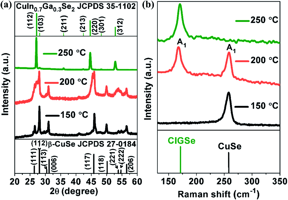 | ||
| Fig. 1 (a) XRD pattern and (b) Raman spectra of CIGSe samples synthesized at different reaction temperature. | ||
FE-SEM micrographs of CIGSe samples synthesized at different reaction temperature are shown in Fig. 2. The sample synthesized at 150 °C showed quasi-hexagonal flake-like particles and their size changed from 0.12 to 0.21 μm. At 200 °C, the observed elongated hexagonal flake-like shape of the particles size was in the range between 0.25 to 0.91 μm. When the reaction temperature increased to 250 °C, the proper hexagonal flake-like shape of the particles was observed with size varying from 1.05 to 1.55 μm and thickness of the flakes was between 90 and 100 nm as shown in Fig. 2(d). Moreover, the size of the nanoparticles on the surface of hexagonal flakes was varied from 80 to 150 nm. EDS composition of CIGSe samples synthesized at different reaction temperature is shown in Fig. 2(e). The sample synthesized at 150 °C exhibited 1.12:0.88 ratio of Cu and Se while In and Ga were absent which is due to the formation of pure CuSe phase at this temperature, as we discussed in the structural analysis (Fig. 1). When the reaction temperature increased to 200 °C, the In and Ga content was detected along with Cu and Se content. As the reaction temperature increased to 250 °C, the observed composition of CIGSe was very close to the targeted value. As the reaction temperature increases, the Cu/(In + Ga) ratio was decreased while Ga/(In + Ga) ratio increased as shown in Fig. 2(f).
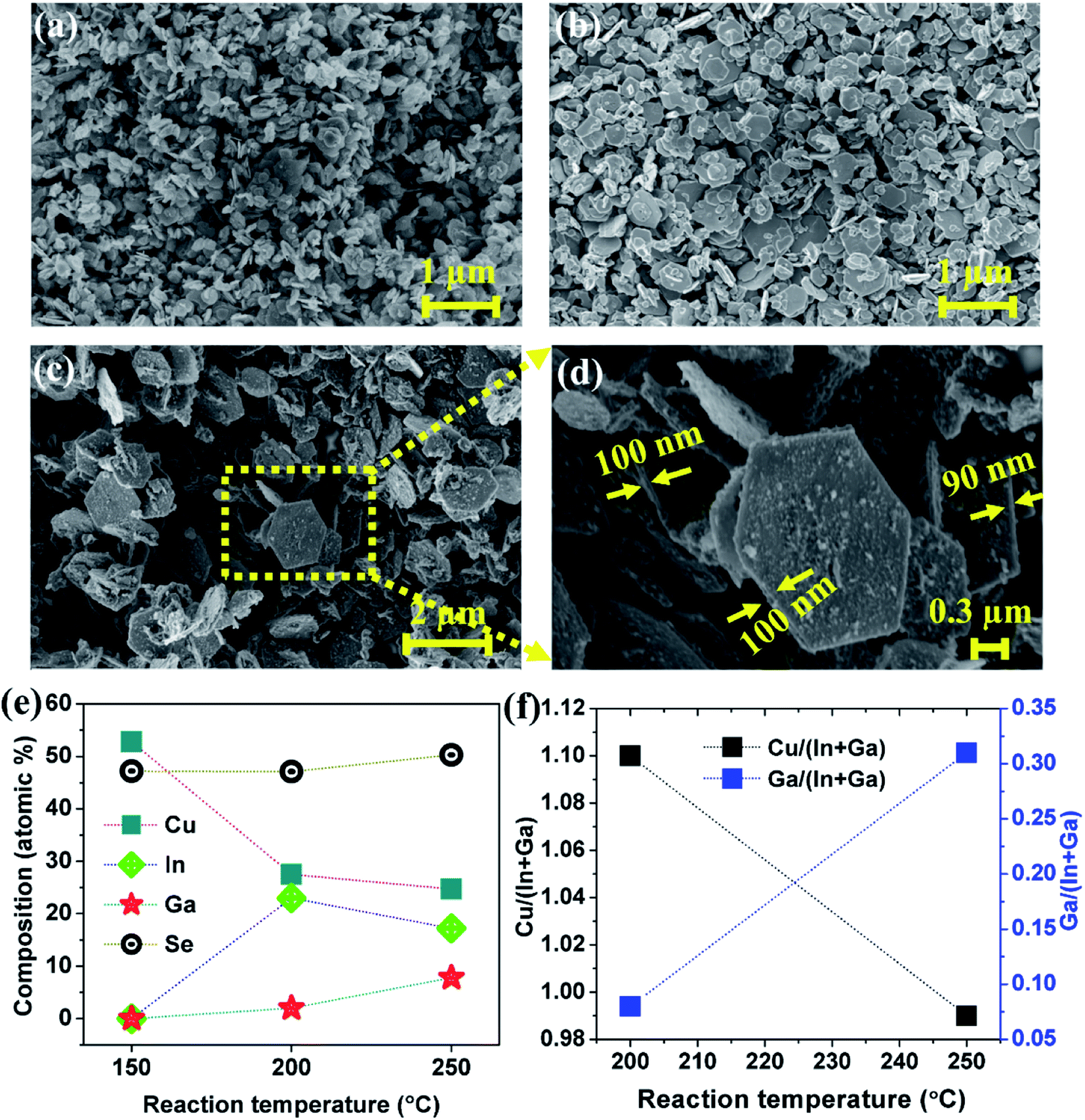 | ||
| Fig. 2 FE-SEM images and EDS composition of CIGSe samples synthesized at different reaction temperature: (a) 150 °C, (b) 200 °C, (c) 250 °C, (d) higher magnification image at 250 °C, (e) EDS composition and (f) Cu/(In + Ga) and Ga/(In + Ga) ratio. | ||
Fig. 3(a) illustrates the quasi-hexagonal flake with a size of 0.20 μm at 150 °C. Fig. 3(b) shows the 1.12:0.88 ratio of Cu and Se (Table 1). Fig. 3(c) inset shows the FFT of β-CuSe. From the HR-TEM image (Fig. 3(c)), the obtained d-spacing values of 0.31 and 0.20 nm were consistent with the (112) and (117) crystal lattice planes of β-CuSe. At 200 °C, Fig. 3(d) shows elongation of hexagonal flakes with size ranging from 0.25 to 0.50 μm. Fig. 3(e) depicts the composition of Cu and Se (1.11:0.89), while Fig. 3(g) shows the composition of Cu:In:Ga:Se (1.10:0.92:0.08:1.90). From Fig. 3(f) and (h), the d-spacing values of 0.31, 0.18 and 0.333 nm were observed, that corresponds to (112) and (118) crystalline planes of β-CuSe and (112) plane of CIGSe respectively (Table 1). At 250 °C, Fig. 3(i) depicts the proper hexagonal flake with a size of ∼1.6 μm. The obtained hexagonal flakes from Fig. 2(c) and 3(i), might be due to the presence of a pair of twin planes in a 6-number fold symmetry. It is worth to mention that CIGSe has only a primitive tetragonal unit system and no hexagonal symmetry axis. Thus, the hexagonal structures are not able to attain without multiple twinning of the primitive axis, which occurs only under the special conditions.27 However, the detailed information about the formation mechanism of CIGSe hexagonal flakes is yet to be fully understood and is under further investigation. Fig. 3(j) shows the material composition of Cu:In:Ga:Se (0.99:0.69:0.31:2.01), which is very close to the desired stoichiometry. From Fig. 3(k), lattice fringes were observed along with the axis of the flake and the calculated d-spacing value of 0.331 nm, ascribed to (112) plane of chalcopyrite CIGSe.28 These results are consistent with the structural analysis (Fig. 1), which elucidates that β-CuSe (starting phase) is formed at low temperature due to the preferential reaction between Cu and Se. Furthermore, the phase transformation occurs from β-CuSe to CIGSe at high temperature since it provides enough energy for the cation inter-diffusion and consequently the starting phase of β-CuSe disappeared.
 | ||
| Fig. 3 (a–c) TEM image and STEM-EDS line scan and HR-TEM image of β-CuSe flake and inset shows the corresponding FFT (at 150 °C), (d) TEM image of β-CuSe and CIGSe flake, (e and f) STEM-EDS and HR-TEM of β-CuSe flake, (g and h) STEM-EDS line scan and HR-TEM of CIGSe flake (at 200 °C), (i–k) TEM image, STEM-EDS line scan and HR-TEM image of CIGSe flake (at 250 °C). | ||
| Reaction temperature | Phase formation | Composition of Cu/In/Ga/Se in atomic ratio% | d-spacing value of HR-TEM (nm) | Corresponding planes | |
|---|---|---|---|---|---|
| 150 °C | β-CuSe | 52.8:47.2 (1.12:0.88) |
0.31 | (112) | |
| 0.20 | (117) | ||||
| 200 °C | Mixed phase of β-CuSe and CIGSe | β-CuSe | 52.7:47.3 (1.11:0.89) |
0.31 | (112) |
| 0.18 | (118) | ||||
| CIGSe | 27.50:23:2:47.09 (1.10:0.92:0.08:1.90) |
0.333 | (112) | ||
| 250 °C | CIGSe | 24.7:17.2:7.8:50.3 (0.99:0.69:0.31:2.01) |
0.331 | (112) | |
Influence of reaction time
Based on the above results, the sample synthesized at 250 °C showed a pure phase CIGSe with the optimum composition. Therefore, this condition is used for further experiments. Herein, the reaction time was varied such as 30, 60, 120 and 150 min and their influences on the structural, compositional, optical and morphological properties were investigated as shown in Fig. 4 and 5. The peaks observed from Fig. 4(a) are consistent with the chalcopyrite crystal structure of CIGSe. As the reaction time increases, the XRD peaks were shifted towards higher 2θ values that can be clearly seen in the magnified view of (112) plane from Fig. 4(b). With increasing the reaction time, A1 mode peak (Fig. 4(c)) was shifted to higher wavenumber. In addition to that, the sample synthesized at 30 min showed a peak at 258 cm−1, matches with A1 mode of CuSe phase that could be due to the Cu-rich composition as can be seen in Fig. 4(e) and (f). The observed peak shift from both XRD and Raman measurements are due to an increment in the Ga content and Ga/(In + Ga) ratio as can be seen in Fig. 4(e) and (f). Therefore, the larger size In atoms are replaced with smaller size Ga atoms, leads to decrement in the lattice constants a and c with respect to reaction time (Fig. 4(d)), that reduces the unit cell volume.4 UV-VIS-NIR absorption spectra (Fig. 5(g)) were shifted towards lower wavelength as the reaction time increases. The Tauc relation is used to calculate the optical band gap by extrapolating the (αhν)2 vs. hν as shown in Fig. 4(h). The obtained band gap values of the samples synthesized at 30, 60, 120 and 150 min were 1.10, 1.19, 1.25 and 1.28 eV respectively. The increment in the band gap values is directly proportional to the Ga content and Ga/(In + Ga) ratio which is in good accordance with the structural and compositional results. The obtained band gap of 1.25 eV at 120 min is desirable for the photovoltaic applications.29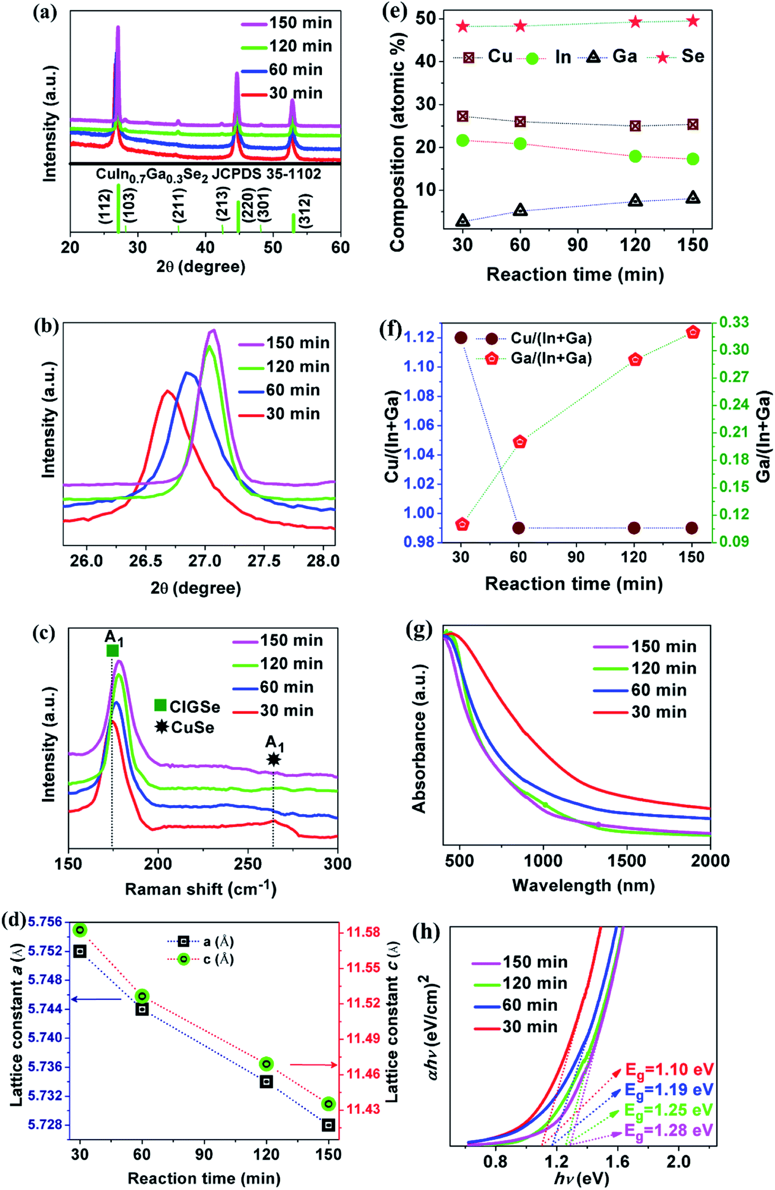 | ||
| Fig. 4 CIGSe samples synthesized at different reaction time: (a) XRD pattern, (b) magnified view of (112) plane, (c) Raman spectra, (d) lattice constants a and c, (e) EDS composition, (f) Cu/(In + Ga) and Ga/(In + Ga) ratio, (g) UV-VIS-NIR absorption spectra and (h) Tauc plots of (αhν)2 versus hν. | ||
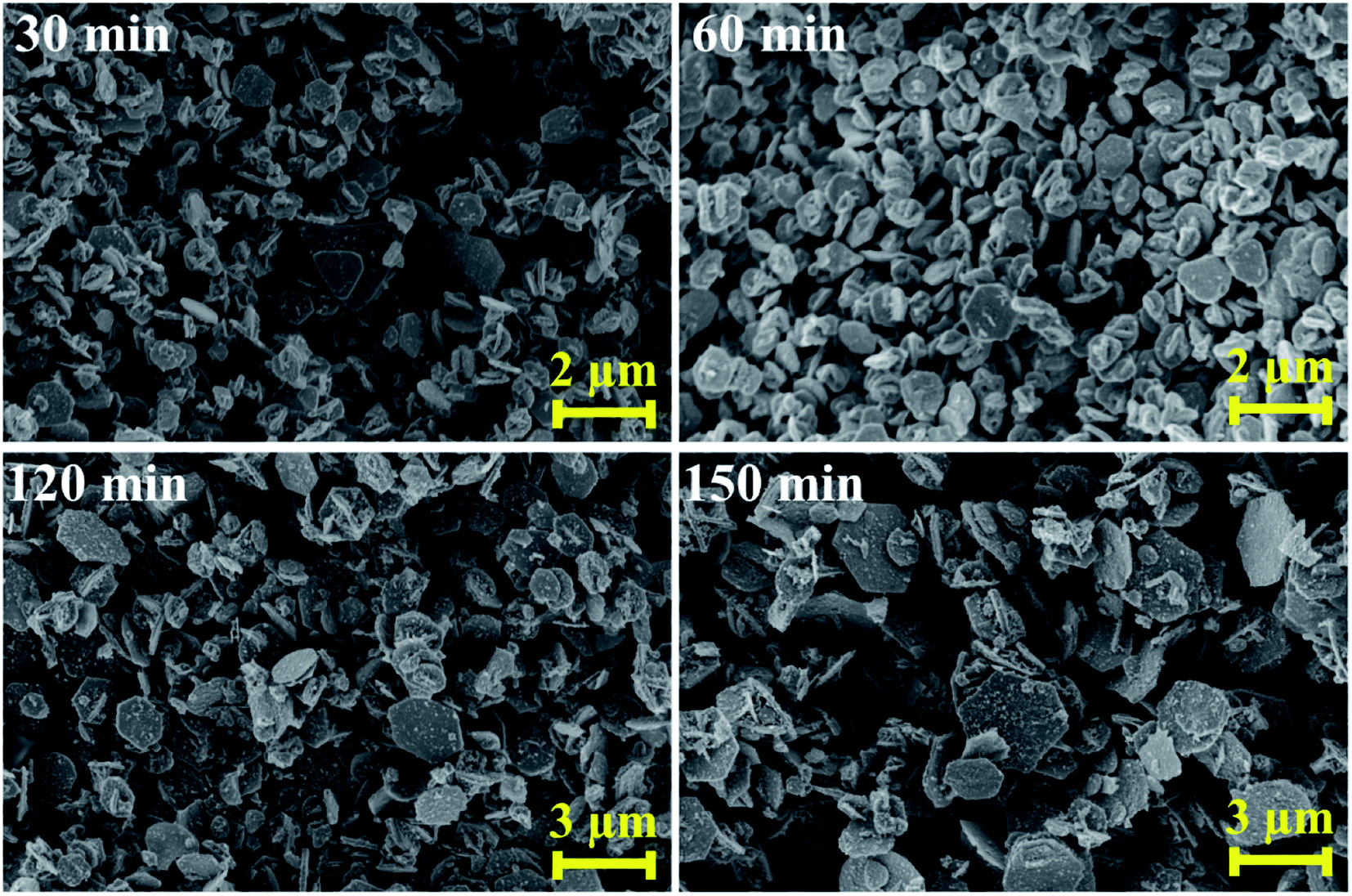 | ||
| Fig. 5 FE-SEM images of CIGSe samples synthesized at different reaction time. | ||
FE-SEM images of CIGSe samples synthesized at different reaction time are shown in Fig. 5. Different shape of crystals such as regular, triangle, quasi hexagonal and hexagonal with inhomogeneous size distribution were observed. The irregular shape and broad size distribution could be due to differences in the reactivity of precursors that is responsible for the inhomogeneous nucleation and growth.30 As the reaction time increases, the size of the crystals increased from 0.9 to 3.1 μm due to the Ostwald ripening process31 in which, large crystals are grown by the dissolution of smaller crystals. Hence, the results revealed that the CIGSe sample synthesized at 120 min is the optimum time to attain the pure phase, targeted composition with a band gap energy of 1.25 eV, which indicates that these microcrystals are highly suitable to be used as absorber material in low-cost thin film solar cells.
Based on the above results, we propose a plausible growth mechanism of CIGSe MCs by one-pot heating-up method which is illustrated in Scheme 1.
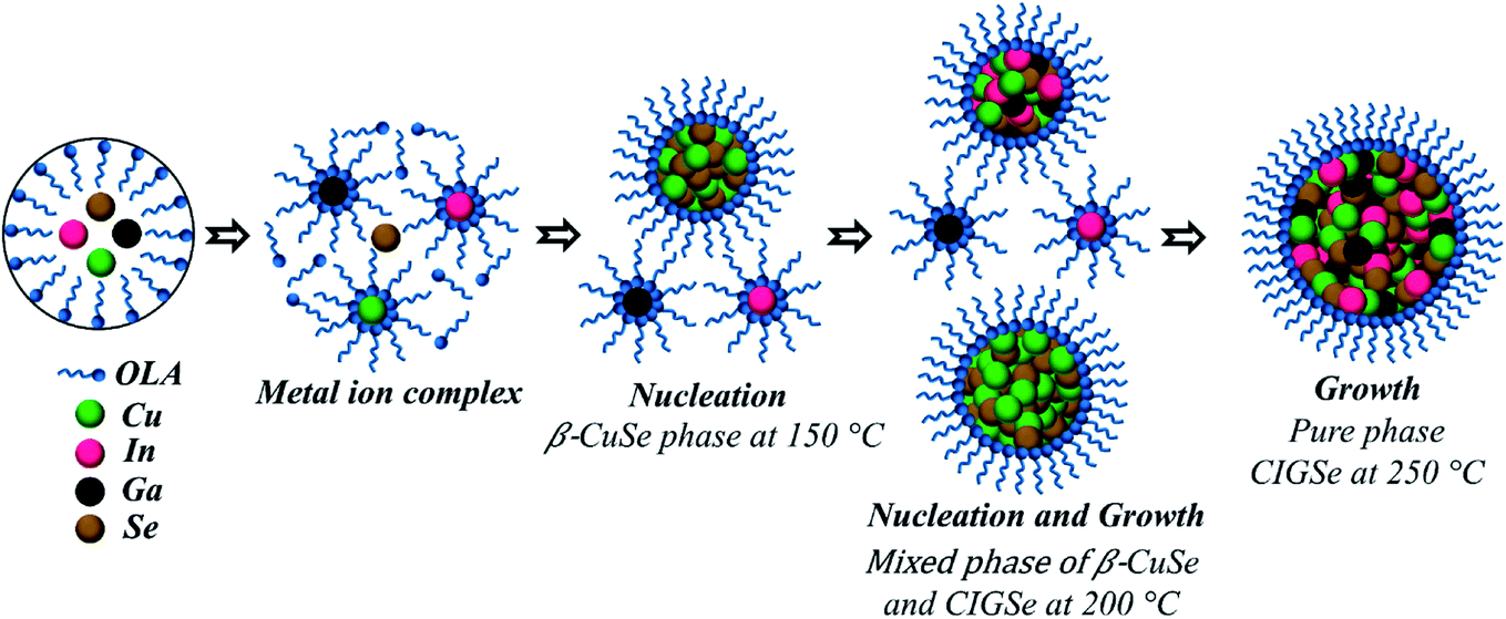 | ||
| Scheme 1 Evolution pathway of CIGSe MCs synthesized via the one-pot heating-up method. | ||
(1) The reaction is initiated by adding all the metal precursors and elemental selenium into OLA and then heated at a targeted temperature. The metal–OLA complexes such as Cu–OLA, In–OLA and Ga–OLA were formed at the beginning of a reaction (150 °C). Later, Cu–OLA complexes get decomposed and then monomers containing Cu+ ions get released, that reacts with Sex2− ions resulting from the dissolution and reduction of Se by OLA, thus forming an orthorhombic crystal structure of β-CuSe which is evident from the structural analysis (Fig. 1). As stated in hard–soft acid–base theory, the elemental ions are generally categorized as acids and bases depending on their capability either to accept or donate electrons. These acids and bases are further categorized as soft and hard according to their electronegativity, polarizability and oxidation states.32 Thus, the soft base of Se reacts with a soft acid of Cu+, instead of hard acids such as Ga3+ and In3+, forming initially β-CuSe crystalline nuclei33 at low temperature and then followed by the oriented growth of seeds. OLA not only acts as an efficient stabilizing ligand but also acts like a template-guide for the preferential growth of quasi-hexagonal orientation of β-CuSe. The hexagonal flake-like shape of β-CuSe is consistent with the literature.23 There is no evidence for the formation of In–Se or Ga–Se phases at this stage which clearly indicates that the In–OLA and Ga–OLA complexes are more stable. The reason behind this is that 1 mmol of CuCl reacts with 2 mmol of OLA, whereas each mmol of ions in the InCl3 and GaCl3 could form coordinate bonds with 3 or more mmol of OLA.32
(2) As the reaction temperature raised to 200 °C, both Ga3+ and In3+ ions are set free. There is an inward diffusion of both these ions into the as-formed β-CuSe and a partial outward diffusion of Cu+ ions, that leads to the formation of CIGSe.34 Cu(I) ions in the CuSe have high mobility which can facilitate an exchange with other cations such as Ga3+ and In3+ at relatively high reaction temperature. The conversion from β-CuSe to CIGSe is a consequence of lattice distortion which can be accomplished by a low energy barrier. The uncontrolled outward diffusion of Cu+ and the limited supply of Ga3+ and In3+ ions leads to a prolonged growth stage causing elongation of β-CuSe as can be seen in Fig. 2(b) and 3(d). Moreover, in few particles, the intercalation of cations into CuSe is so enormous that there is a transformation of the geometry from quasi-hexagonal to elongated structures to irregular to proper hexagonal ones, which is confirmed from the Fig. 2(a)–(c). Hence, the observed mixed phase of β-CuSe and CIGSe is the resultant of incomplete reaction taking place at this temperature, that can also be deduced from the structural analysis (Fig. 1).
(3) Pure phase formation of CIGSe was obtained at 60 min as shown in Fig. 4(a) and (c). The complete chemical transformation occurred from β-CuSe to CIGSe suggests that the high reaction temperature (250 °C) provides more energy for cation inter-diffusion and thus expels the starting phase of β-CuSe. However, the In-rich and Ga-poor composition were observed from Fig. 4(e) and (f), because Ga3+ is a harder acid in comparison with In3+ as In3+ is more electronegative than Ga3+,32 In3+ could be incorporated easily into β-CuSe. By prolonging the reaction time, Ga3+ ions released abundantly from Ga–OLA complexes and formation of pure phase CIGSe with targeted composition was confirmed from the Fig. 4(f).
Large-scale synthesis of CIGSe MCs
In order to test the scalable process, the precursors and solvent volume were increased to 10-fold compared to the small-scale synthesis as mentioned in the experimental part. Fig. 6 summarize the results for gram-scale production prepared using Cu:In:Ga:Se precursor ratio of 1:0.7:0.3:2 in 100 mL OLA under a nitrogen atmosphere at 250 °C for 120 min. XRD patterns, Raman spectrum, HR-TEM image and SAED pattern exhibited the chalcopyrite crystal structure of pure phase CIGSe. From the absorption spectrum (Fig. 6(c)), the band gap energy of 1.25 eV was determined by extra plotting hν versus (αhν)2 as shown in Fig. 6(d). This is consistent with the small-scale results. From Fig. 6(e) and (i), the hexagonal flake-like shape of CIGSe was observed with size ranging from 1.05 to 1.65 μm. EDS elemental mapping of hexagonal flakes revealed that the Cu, In, Ga, and Se elements were homogenously distributed [Fig. 6(k)–(n)]. The targeted composition of Cu:In:Ga:Se (1:0.7:0.3:2) was obtained from Fig. 6(h).
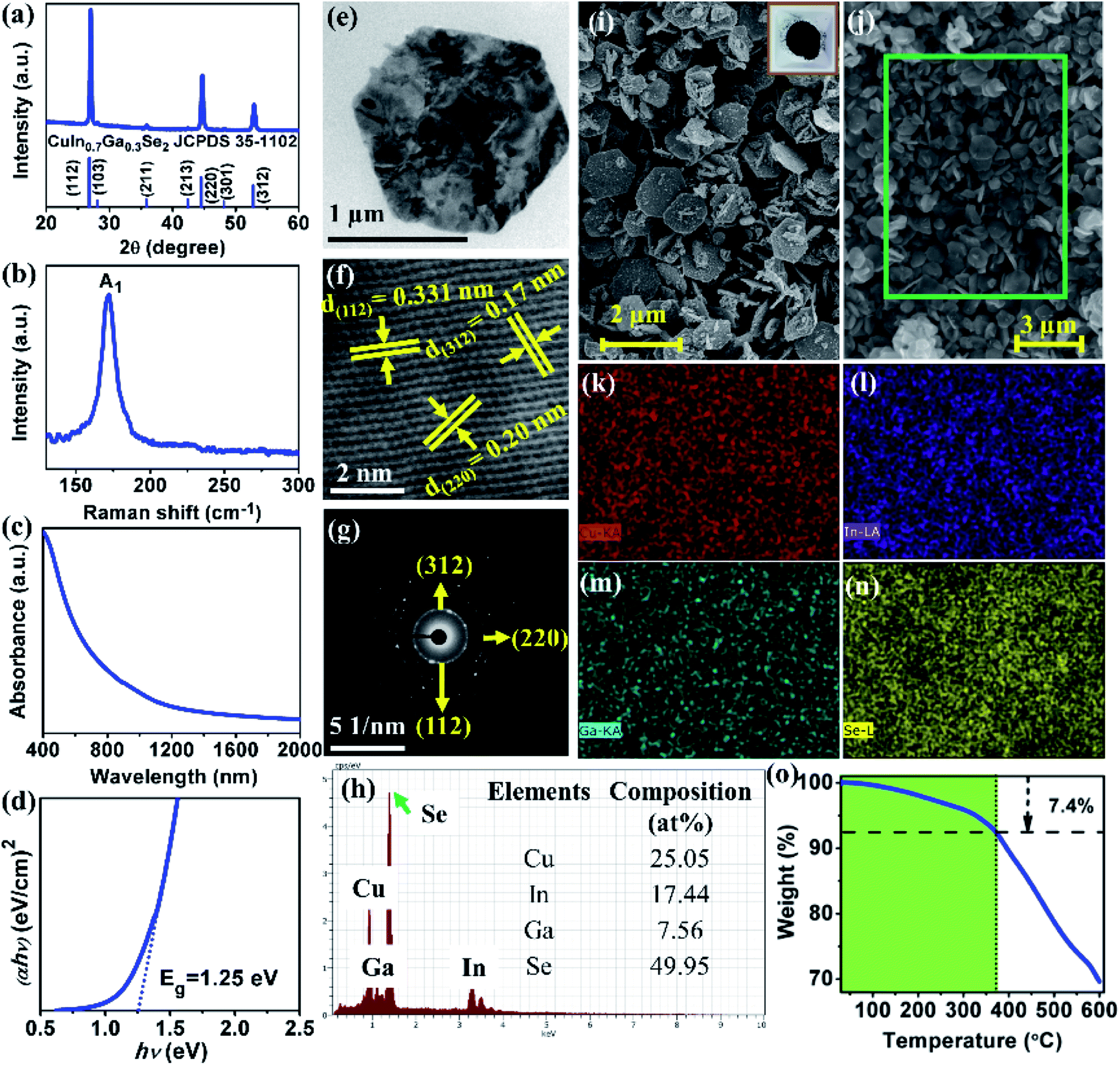 | ||
| Fig. 6 Large-scale synthesis of CIGSe at 250 °C for 120 min. (a) XRD pattern, (b) Raman spectrum, (c) UV-VIS-NIR absorption spectrum, (d) band gap spectrum, (e) TEM micrograph, (f) HR-TEM image, (g) SAED pattern, (h) EDS spectrum, (i) FE-SEM micrograph, (j) FE-SEM EDS mapping (green rectangular is the selected area), (k–n) EDS mapping and (o) TGA analysis. | ||
Furthermore, the synthesis yield is an essential feature of large-scale synthesis of CIGSe MCs which is calculated by comparing the total weight of the final product and the initial precursors.34 TGA analysis was used to estimate the contribution of organic solvent (OLA) to the weight of the final product. Based on the TGA analysis (Fig. 6(o)), the weight loss of OLA was around 7.4% over the temperature ranging from 30 to 370 °C, which was subsequently subtracted from the weight of the final product and the calculated synthesis yield was found to be 90%. Thus, the results revealed the possibility of producing CIGSe MCs in gram-scale with good control over the pure phase, morphology, particle size, band gap energy and composition by one-pot heating-up method.
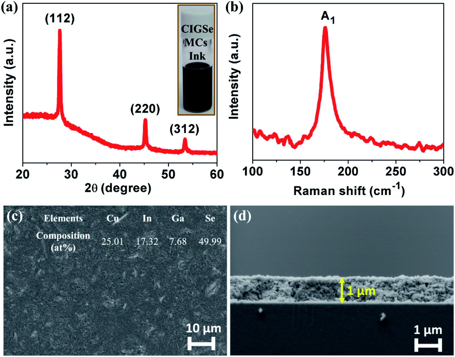
Properties of CIGS MCs thin films
As can be seen in Fig. 7(a) inset, the ink was formulated by readily dispersing the synthesized CIGSe MCs in ethanol and coated as thin films to evaluate their suitability as an absorber layer for solar cell applications. The structural, morphological, compositional, electrical and photoresponse properties of CIGSe MCs thin films were investigated. Fig. 7(a) and (b) showed similar structural properties to the powder, which proves that the possibility of transferring powder into thin films. The crack free thin film and densely packed grains along with the thickness of 1 μm were observed from the Fig. 7(c) and (d). The obtained chemical composition of Cu:In:Ga:Se (0.99:0.71:0.29:2.01) from Fig. 7(c) inset is very close to the powder composition.
 | ||
| Fig. 7 (a) XRD pattern, (b) Raman spectrum, (c) FE-SEM image (planar) and the inset shows the EDS composition and (d) cross-sectional image of drop casted CIGSe MCs thin films. | ||
Electrical properties of CIGSe thin films greatly plays an important role in solar cell performance. Therefore, the CIGSe thin films with microsized grains, p-type conductivity, carrier concentration in the order of 1016 to 1018 cm−3, and Ga/(Ga + In) ratio ∼0.34,35 are required to obtain the high efficiency solar cells. The electrical properties of CIGSe thin films are strongly affected by its grain size, composition and deposition process as shown in Table 2. However, it is worth to mention that only a few reports are available on the electrical properties of CIGSe thin films by the ink coating approach. The resistivity, carrier concentration and mobility of CIGSe MCs thin films were 0.37 Ω cm, 2 × 1017 cm−3 and 11.92 cm2 V−1 s−1 respectively. The CIGSe MCs thin films showed lower resistivity along with an optimum carrier concentration. Among other reports, the mobility of CIGSe MCs thin film is very high and increased by 4 times as compared to CIGSe NCs thin film.4,36 This could be due to an increment in the grain size, which reduces the grain boundary scattering, whereas nanosized grains causing higher number of grain boundaries that prevent the flow of charge carriers. These findings confirmed that the coating of thin films using CIGSe MCs ink is highly suitable to be used as an absorber layer.
| Thin films | Deposition process | Conductivity type | Carrier concentration (cm−3) | Resistivity (Ω cm) | Mobility (cm2 V−1 s−1) | Ref. |
|---|---|---|---|---|---|---|
| Cu0.94(In0.7Ga0.3)Se2 | 3-Stage co-evaporation | p | 2.1 × 10¹⁵ | 29.3 | — | 37 |
| Cu(In0.7Ga0.3)Se2 | Pulsed laser deposition (at 500 °C) | p | 6.79 × 10¹⁸ | 0.488 | 1.89 | 38 |
| CuInSe2 | Nanoplate ink coating | p | 1.4 × 10¹⁹ | 0.9055 | 0.479 | 39 |
| Cu(In0.75Ga0.25)Se2 | NCs ink coating | p | 1.95 × 10¹⁸ | 2.41 | 2.92 | 4 |
| Cu(In0.70Ga0.30)Se2 | NCs ink coating | p | 2 × 10¹⁷ | 2.03 | 3.24 | 36 |
| Cu(In0.70Ga0.30)Se2 | MCs ink coating | P | 2 × 10¹⁷ | 0.37 | 11.92 | Present study |
Photoconductivity measurement is an important aspect to study the material appropriateness for solar cell applications. The generation and transportation of charge carriers are the main processes involved in the photoconductive of a semiconductor. When the photoconductor absorbs the light, resulting in the generation of free electrons excited from valence band to conduction band while holes are generated in the valence band concurrently. When the electric field applies through the materials, both electrons and holes are transported through materials, consequently the electric current is produced in the circuit which enhances the conductivity of semiconductor.40 Photoconductivity of the CIGSe MCs thin film was studied, both in the dark and under the illumination of light. As shown in Fig. 8, the linear nature of I–V curve suggests the better ohmic contact between Au (contact) and CIGSe MCs.41 Under illumination, the obtained linear and stable nature of I–V curve accordance with the absorption of light, generation of charge carriers (electrons and holes) and transportation of charge carriers, enhances the photoconductivity in comparison with dark. The photoconductivity can be expressed by ΔI i.e. the current difference between the dark and under illumination of light at a given bias voltage.42 The calculated photocurrent of CIGSe MCs thin film was found to be 4.39 mA. The CIGSe MCs thin film showed the photocurrent in the mA whereas CIGSe NCs thin film showed photocurrent in the μA.4,36 The obtained photocurrent (3-orders magnitude high) of thin film prepared from MCs ink could be due to the low density of grain boundaries because of larger (∼1.5 μm) sized grains, which are beneficial to reduce the recombination rate of charge carriers. Thin films made from CIGSe NCs ink showed lower photocurrent, due to the presence of smaller (<50 nm) sized grains leading to a high density of grain boundaries that can serve as recombination centers.
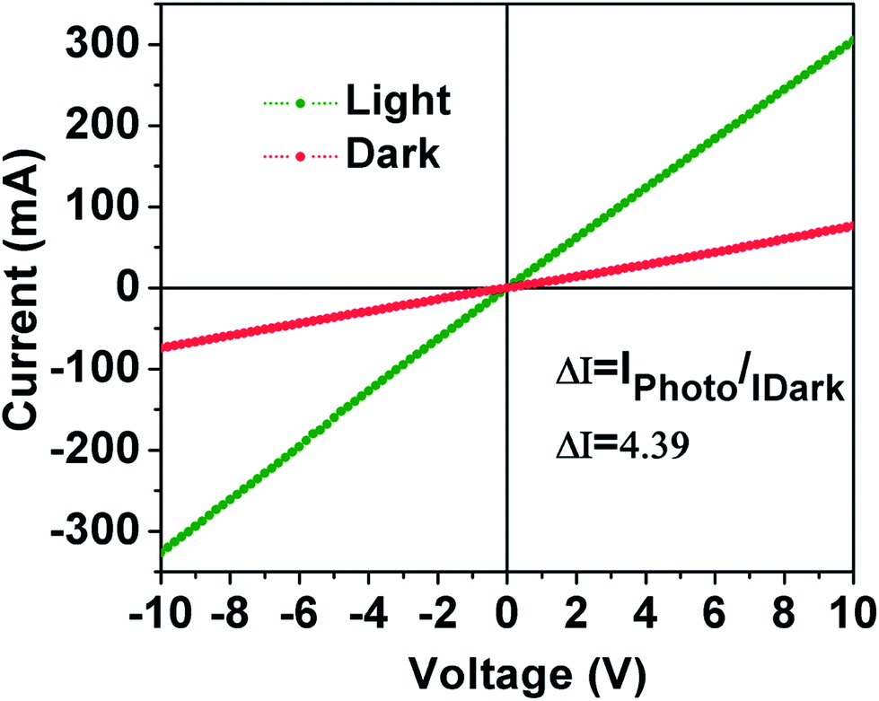 | ||
| Fig. 8 I–V curve of drop casted CIGSe MCs thin film. | ||
Solar cell performance
As a proof of concept, thin films casted from CIGSe NCs36 and MCs ink were tested as an absorber layer in solar cells fabricated with a conventional structure of Mo/CIGSe/CdS/i-ZnO/Al–ZnO/Ag. The thickness of Mo, CIGSe, CdS, i-ZnO and Al–ZnO were 950, 1000, 50, 50 and 150 nm respectively. Fig. 9 shows the J–V characteristic measured under the illumination of AM 1.5G solar simulator (100 mW cm−2) and the total area of solar cells was 0.4 cm2. From the figure, the CIGSe MCs thin films showed substantial enhancement in the open circuit voltage (Voc), short circuit current density (Jsc) and fill factor (FF). Besides, the CIGSe MCs thin film demonstrated the PCE of 0.59% which is 14.75 times higher than CIGSe NCs thin film. This is because of microsized grains reduced the grain boundaries, scattering centers and traps for photogenerated carriers. According to the results, we believe that, microsized grains downgrades the interfacial area that suppresses charge trapping and recombination.43 In addition to that, photogenerated carriers could be easily collected without massive encounters with impurities and bulk defects44 since microsized grains have higher mobility and lower bulk defects. However, the achieved PCE from CIGSe MCs is too low as compared to the vacuum process.6 The PCE of solar cells could be enhanced in the future by optimizing process parameters of other layers such as CdS, i-ZnO and Al–ZnO which plays an imperative role in the process of converting solar energy into electrical energy.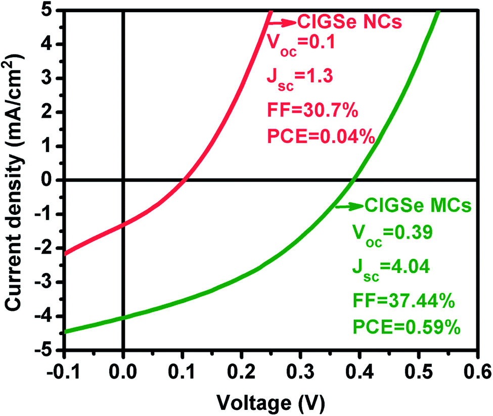 | ||
| Fig. 9 J–V curve of CIGSe solar cells under the illumination. | ||
Conclusion
In summary, quaternary CIGSe MCs were synthesized using a facile one-pot heating-up method. The formation mechanism evolved from binary β-CuSe to CIGSe by gradual incorporation of In3+ and Ga3+ ions into the β-CuSe crystal lattice. The large-scale synthesis was performed using the same procedure by increasing the amount of precursors and solvent to 10-fold, which showed a high reaction yield of 90% while maintaining control over the pure phase, band gap energy, composition, morphology and particle size. Moreover, the CIGSe MCs ink was formulated and drop casted as thin films. The electrical and photoresponse properties of CIGSe MCs thin film were greatly enhanced. The applicability of CIGSe MCs as an absorber layer in thin film solar cells was tested which demonstrated the PCE of 0.59%. In future, the proposed approach in this work, could give a new vision to scale-up the solution process for the preparation of other light absorbing semiconductor materials with microsized grains for solar cell applications.Conflicts of interest
There are no conflicts to declare.Acknowledgements
Authors acknowledge the CeMIE-Sol, P-55 for their partial financial support. Dr Latha Marasamy acknowledges the postdoctoral fellowship grant from Fondo Sectorial CONACYT-Secretaria de Energia-Sustentabilidad Energetica 2018–2019. We thank Adolfo Tavira Fuentes (XRD), Alejandra Garcia-Sotelo (Raman), Angela Gabriela Lopez Fabian (UV-VIS-NIR), Jorge Roque De la Puente (FESEM & EDS-LANE), Alvaro Angeles Pascual (HRTEM & HAADF-STEM from LANE), Miguel Ángel Luna Arias (Hall-effect measurement) and Miguel Galván Arellano (I–V measurements) for their technical support.References
- G. R. Uhm, S. Y. Jang, Y. H. Jeon, H. K. Yoon and H. Seo, RSC Adv., 2014, 4, 28111–28118 RSC.
- S. Kang, R. Nandi, J. Sim, J. Jo, U. Chatterjee and C. Lee, RSC Adv., 2017, 7, 48113–48119 RSC.
- A. S. Kshirsagar, P. V. More and P. K. Khanna, RSC Adv., 2016, 6, 86137–86150 RSC.
- M. Latha, R. A. Devi and S. Velumani, Opt. Mater., 2018, 79, 450–456 CrossRef CAS.
- P. U. Londhe, A. B. Rohom and N. B. Chaure, RSC Adv., 2015, 5, 89635–89643 RSC.
- P. Jackson, R. Wuerz, D. Hariskos, E. Lotter, W. Witte and M. Powalla, Phys. Status Solidi RRL, 2016, 10, 583–586 CrossRef CAS.
- A. H. Cheshmekhavar, A. R. Mahjoub, H. Fakhri and M. Dehghani, RSC Adv., 2015, 5, 97381–97390 RSC.
- M. Kaelin, D. Rudmann, F. Kurdesau, H. Zogg, T. Meyer and A. N. Tiwari, Thin Solid Films, 2005, 480–481, 486–490 CrossRef CAS.
- Y. J. Hwang, J. Kim, D. Kim and B. Koun, RSC Adv., 2015, 5, 103439–103444 RSC.
- M. R. Golobostanfard and H. Abdizadeh, RSC Adv., 2016, 6, 11903–11910 RSC.
- M. G. Panthani, V. Akhavan, B. W. Goodfellow, J. P. Schmidtke, L. Dunn, A. Dodabalapur, P. F. Barbara and B. A. Korgel, Prog. Photovoltaics, 2008, 2, 16770–16777 Search PubMed.
- T. B. Harvey, I. Mori, C. J. Stolle, T. D. Bogart, D. P. Ostrowski, M. S. Glaz, J. Du, D. R. Pernik, V. A. Akhavan, H. Kesrouani, D. A. Vanden Bout and B. A. Korgel, ACS Appl. Mater. Interfaces, 2013, 5, 9134–9140 CrossRef CAS.
- G. S. Jung, S. H. Mun, D. Shin, R. B. V. Chalapathy, B. T. Ahn and H. Kwon, RSC Adv., 2015, 5, 7611–7618 RSC.
- Q. Guo, G. M. Ford, R. Agrawal and H. W. Hillhouse, Prog. Photovoltaics, 2013, 21, 64–71 CAS.
- S. M. McLeod, C. J. Hages, N. J. Carter and R. Agrawal, Prog. Photovoltaics, 2015, 23, 1550–1556 CAS.
- M. Wang, S. K. Batabyal, Z. Li, D. Li, S. G. Mhaisalkar and Y. M. Lam, RSC Adv., 2013, 3, 9829–9834 RSC.
- V. Nalla, J. C. W. Ho, S. K. Batabyal, Y. Wang, A. I. Y. Tok, H. Sun, H. Wong and N. Zheludev, RSC Adv., 2014, 4, 58372–58376 RSC.
- S. R. Thomas, C. Chen, M. Date, Y. Wang, H. Tsai, M. Wang and Y. Chueh, RSC Adv., 2016, 1, 60643–60656 RSC.
- M. Wang, S. K. Batabyal, H. M. Lim, Z. Li and Y. M. Lam, J. Alloys Compd., 2015, 618, 522–526 CrossRef CAS.
- M. Rohini, P. Reyes, S. Velumani, M. Latha, G. Oza, I. Becerril-Juarez and R. Asomoza, Mater. Sci. Semicond. Process., 2015, 37, 151–158 CrossRef CAS.
- M. Latha, R. A. Devi, M. Rohini, P. Reyes-Figueroa, I. G. Becerril-Juarez, S. Velumani, J. Yi and G. Oza, J. Nanosci. Nanotechnol., 2015, 15, 8388–8394 CrossRef CAS PubMed.
- B. Li, Y. Xie, J. Huang and Y. Qian, Adv. Mater., 1999, 11, 1456–1459 CrossRef CAS.
- Y. Xie, X. Zheng, X. Jiang, J. Lu and L. Zhu, Inorg. Chem., 2002, 41, 387–392 CrossRef CAS.
- Z. Wei, S. Senthilarasu, M. V Yakushev, W. Martin and H. M. Upadhyaya, RSC Adv., 2014, 4, 5141–5147 RSC.
- Q. Nian, M. Y. Zhang, D. Lin, S. Das, C. Shin and G. J. Cheng, RSC Adv., 2015, 5, 57550–57558 RSC.
- F. W. D. S. Lucas, A. R. F. Lima and L. H. Mascaro, RSC Adv., 2015, 5, 18295–18300 RSC.
- E. J. Lee, I. Nam, J. Yi and J. H. Bang, J. Mater. Chem. A, 2015, 3, 3500–3510 RSC.
- S. N. Malik, S. Mahboob, N. Haider, M. A. Malik and P. O'Brien, Nanoscale, 2011, 3, 5132–5139 RSC.
- N. Oulmi, A. Bouloufa, A. Benhaya and R. Mayouche, Materials for Renewable and Sustainable Energy, 2019, 2, 1–8 Search PubMed.
- Q. Guo, S. J. Kim, M. Kar, W. N. Shafarman, R. W. Birkmire, E. A. Stach, R. Agrawal and H. W. Hillhouse, Nano Lett., 2008, 8, 2982–2987 CrossRef CAS PubMed.
- N. Pradhan, D. Reifsnyder, R. Xie and J. Aldana, J. Am. Chem. Soc., 2007, 129, 9500–9509 CrossRef CAS.
- M. Ahmadi, S. S. Pramana, L. Xi, C. Boothroyd, Y. M. Lam and S. Mhaisalkar, J. Phys. Chem. C, 2012, 116, 8202–8209 CrossRef CAS.
- W. H. Hsu, H. I. Hsiang, Y. L. Chang, D. T. Ray and F. S. Yen, J. Am. Ceram. Soc., 2011, 94, 3030–3034 CrossRef CAS.
- E. Dilena, Y. Xie, R. Brescia, M. Prato, L. Maserati, R. Krahne, A. Paolella, G. Bertoni, M. Povia, I. Moreels and L. Manna, Chem. Mater., 2013, 25, 3180–3187 CrossRef CAS.
- I. Repins, M. A. Contreras, B. Egaas, C. Dehart, J. Scharf and C. L. Perkins, Prog. Photovoltaics, 2008, 235–239 CAS.
- M. Latha, R. Aruna-devi, S. Velumani, J. Santoyo-salazar and F. De Moure-flores, Adv. Powder Technol. DOI:10.1016/j.apt.2019.09.005.
- L. Zhang, F. Liu, F. Li, Q. He, B. Li and C. Li, Sol. Energy Mater. Sol. Cells, 2012, 99, 356–361 CrossRef CAS.
- C. Nicolaou, A. Zacharia, G. Itskos and J. Giapintzakis, Sol. Energy, 2018, 174, 793–802 CrossRef CAS.
- H. Liu, Z. Jin, W. Wang and J. Li, CrystEngComm, 2011, 13, 7198–7201 RSC.
- J. Henry, P. Prema, D. P. Padiyan, K. Mohanraj and G. Sivakumar, New J. Chem., 2016, 40, 2609–2618 RSC.
- M. Li, W. Zhou, J. Guo, Y. Zhou, Z. Hou, J. Jiao, Z. Zhou, Z. Du and S. Wu, J. Phys. Chem. C, 2012, 116, 26507–26516 CrossRef CAS.
- R. Aruna-Devi, M. Latha, S. Velumani, J. Santos-Cruz, B. Murali, J. A. Chávez-Carvayar, F. A. Pulgarín-Agudelo and O. Vigil-Galán, RSC Adv., 2019, 9, 18420–18428 RSC.
- W. Nie, H. Tsai, R. Asadpour, J. C. Blancon, A. J. Neukirch, G. Gupta, J. J. Crochet, M. Chhowalla, S. Tretiak, M. A. Alam, H. L. Wang and A. D. Mohite, Science, 2015, 347, 522–526 CrossRef CAS.
- Z. Liang, S. Zhang, X. Xu, N. Wang, J. Wang, X. Wang, Z. Bi, G. Xu, N. Yuan and J. Ding, RSC Adv., 2015, 5, 60562–60569 RSC.
| This journal is © The Royal Society of Chemistry 2019 |