
 Open Access Article
 This Open Access Article is licensed under a Creative Commons Attribution-Non Commercial 3.0 Unported Licence
Large bandgap quantum spin Hall insulator in methyl decorated plumbene monolayer: a first-principles study
Shoaib Mahmud and
Md. Kawsar Alam *
*
Department of Electrical and Electronic Engineering, Bangladesh University of Engineering and Technology, Dhaka 1205, Bangladesh. E-mail: kawsaralam@eee.buet.ac.bd; kawsar.alam@alumni.ubc.ca
First published on 19th December 2019
Abstract
Topologically protected edge states of 2D quantum spin Hall (QSH) insulators have paved the way for dissipationless transport. In this regard, one of the key challenges is to find suitable QSH insulators with large bandgaps. Group IV analogues of graphene such as silicene, germanene, stanene, plumbene etc. are promising materials for QSH insulators. This is because their high spin–orbit coupling (SOC) and large bandgap opening may be possible by chemically decorating these group IV graphene analogues. However, finding suitable chemical groups for such decoration has always been a demanding task. In this work, we investigate the performance of a plumbene monolayer with –CX3 (X = H, F, Cl) chemical decoration and report very large bandgaps in the range of 0.8414 eV to 0.9818 eV with spin–orbit coupling, which is much higher compared to most other topological insulators and realizable at room temperature. The  topological invariants of the samples are calculated to confirm their topologically nontrivial properties. The existence of edge states and topological nontrivial property are illustrated by investigating PbCX3 nanoribbons with zigzag edges. Lastly, the structural and electronic stability of the topological materials against strain are demonstrated to extend the scope of using these materials. Our findings suggest that these derivatives are promising materials for spintronic and future high performance nanoelectronic devices.
Introduction
Topological insulators are new states of matter having a bulk bandgap like ordinary insulators and unique protected edge states which allow dissipationless transport.1,2 The edge states of topological insulators are protected by time-reversal symmetry which safeguards them from back scattering in the presence of impurity.3 2D topological insulators are particularly fascinating due to their linear dispersion of the energy band near the Fermi level, leading to high Fermi velocity and mobility.4 HgTe/CdTe5 and InAs/GaSb6 heterostructures have been experimentally proven to be 2D topological insulators. However, the bandgaps are so small that topological edge states can only be found below 10 K. With the discovery of the quantum spin Hall effect in graphene, a new gateway to topological insulators was opened by Kane and Mele.7 Though the band gap in graphene is still very small (10−3 meV),8 2D materials having honeycomb structure like graphene have been shown to have remarkable spin–orbit coupling and linear dispersion of energy near Fermi level in them.9–12 The larger spin–orbit coupling leads to higher bandgap in the bulk and linear dispersion of energy causes high Fermi velocity of electron, which makes such materials suitable for device application.Group IV analogues of graphene (silicene, germanene, stanene, plumbene) with notable spin–orbit coupling, have recently drawn noteworthy attention due to the presence of Dirac fermion in them, similar to graphene.9,13–17 Nonetheless, reported bandgap opening due to spin–orbit coupling in silicene (1.55 meV),18 germanene (23.9 meV),18 stanene (73.5 meV)19 are not sufficient for room temperature operation. On the other hand, monolayer plumbene has drawn attention in recent times particularly due to its large band gap opening at room temperature.20,21 Since plumbene does not show topological nontrivial characteristics normally,15,20 we need additional transformation techniques to have topological nontrivial characteristics in it and take the advantage of this large spin–orbit coupling.
Chemical decoration,20,22–25 application of electric field,26,27 substrate engineering28 and absorption or adsorption adatoms29,30 are among the few techniques that have been used for band gap opening as well as modification of topological properties in group IV monolayers. For the electric field method, the bandgap opening is sometimes too small to operate at room temperature and breakdown electric field of materials constraints the range of applied electric field.31 Also, substrate engineering has the limitation of very small bandgap opening and interaction between materials and the substrate may damage the crystalline structure.20,28 Moreover, doping and molecular adsorption can distort the crystal structure leading to difficulty in fabrication and device integration.30 Chemical decoration is the most appealing method among the mentioned techniques as it offers large bandgap opening while maintaining structural and electronic stability. Thus, chemical decoration in graphene analogues of 2D materials has been a matter of great interest in recent times since they have been reported to offer the highest bulk bandgap for topological insulators.20–22
In this regard, finding a suitable chemical group for chemical decoration to have topological property is the main challenging task. It has been proven theoretically that hydrogen and halogen decoration would provide large bandgap.13,20,32 However, experimental works have been reported showing plasma hydrogenation and fluorination of materials rapidly increase defects and disorders.33,34 Therefore, alkyl and alkyl halide decoration of silicene, germanene, stanene and plumbene are suitable alternatives since such decoration may provide comparable bandgap to that of hydrogenation and halogenation without noticeably increasing the defects and disorders.23,35,36 Methyl derivatives among alkyl groups have shown preferable result in silicene, germanene, stanene and other 2D materials with hexagonal honeycomb structure similar to graphene.4,37–39 For example, methyl decorated silicene, germanene and stanene have shown quantum spin Hall effect at 25%,39 12%38 and 4%4 strain, respectively. However, integrating them into devices using external strain is a very complex process. Quantum spin Hall effect in methyl decorated silicene, germenane and stanene suggest that it is worth exploring the behavior of methyl decorated plumbene (PbCH3), that has remained unexplored, as of yet.
In this work, we have investigated the structural, electronic and topological properties of PbCX3 (X = H, F, Cl) monolayers. The electronic stability and topological invariant of the structures have been determined from formation energy and  topological invariant, respectively. Then, we have performed an orbital analysis to illustrate the origin of bandgap and topological nontriviality. The existence of edge states and topological nontriviality have been demonstrated by analyzing the bandstructures of their respective semi-infinite nanosheet with zigzag edges. The structural and electronic stabilities of these structures against strain have also been analyzed for observing their behavior under strain and examining the suitability of these materials for potential integration in nanodevices.
Methodology and modeling
First-principles calculations based on density functional theory (DFT) was performed using Synopsys Quantumwise ATK simulation package.40 Firstly, a 2D plumbene nanosheet was prepared by cleaving the bulk crystalline plumbene cell whose top view and side view along with crystal unit cell have been shown in Fig. 1.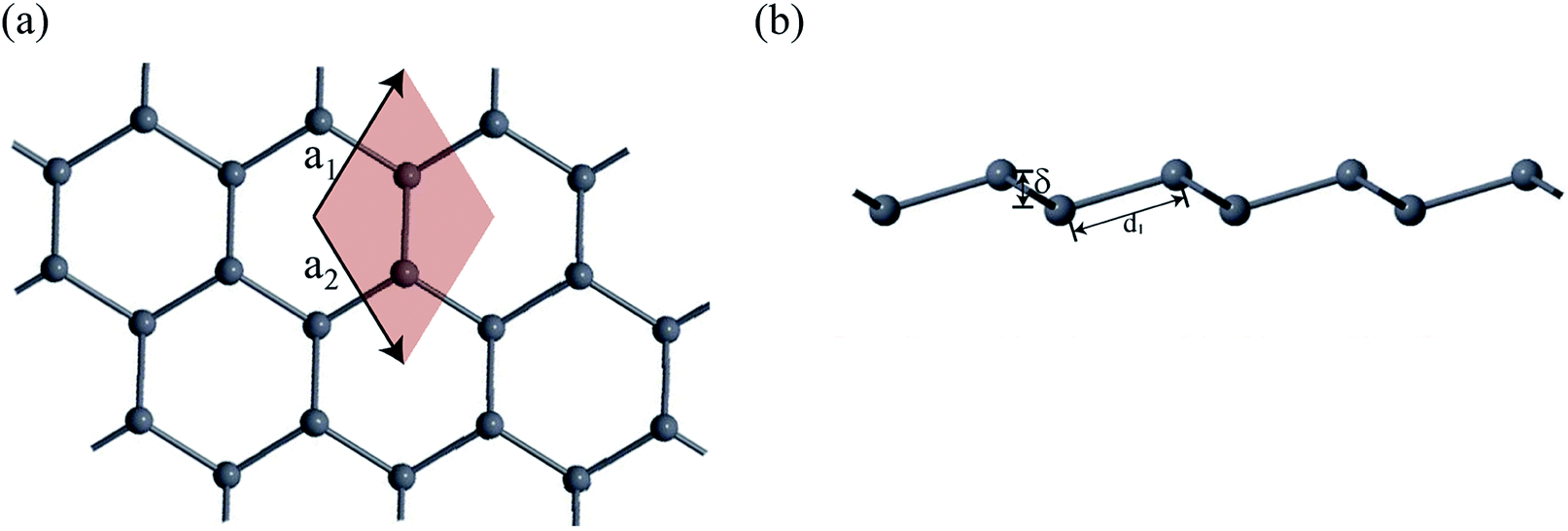 | ||
| Fig. 1 (a) A monolayer nanosheet of plumbene after cleaving bulk crystalline plumbene cell. (b) Side view of the nanosheet showing buckling height (δ) and Pb–Pb bond distance (d1). | ||
Then, the geometry of plumbene monolayer was optimized using Limited-memory Broyden–Fletcher–Goldfarb–Shanno (LBFGS) optimization algorithm.41 Structural relaxation was implemented until force on each atom became less than force tolerance and stress on crystal cell was less than stress error tolerance. In this regard, the linear combination of atomic orbitals (LCAO) calculator was used with generalized gradient approximation (GGA)-Perdew–Burke–Ernzerhof (PBE) exchange–correlation method.42 The self-consistent field (SCF) simulation was continued until it reached the accuracy of iteration control tolerance. The Brillouin zone was sampled by using 9 × 9 × 1 Gamma centered Monkhorst Package.43 The vacuum distance was set to 30 Å which is sufficient to avoid interaction between two parallel layers.20,38 Spin–orbit coupling was included in the calculation using non-collinear spin–orbit interaction method44 and SG15-SO pseudopotential.45 The parameters and their values used in the simulations are given in Table 1.
| Parameter | Value |
|---|---|
| Force tolerance | 0.01 eV Å−1 |
| Stress error tolerance | 0.001 eV Å−3 |
| k-Point sampling | 9 × 9 × 1 |
| Pseudopotential (SOC) | SG15-SO |
| Density mesh cut-off | 125 hartree |
| Iteration control tolerance | 10−5 eV |
| Pseudopotential (without SOC) | PseudoDojo |
| Damping factor | 0.1 |
Next, we decorated the plumbene monolayer sheet with –CX3 (X = H, F, Cl) groups and repeated the geometry optimization process using the same procedure. In order to verify electronic stability of the decorated structures, the formation energy (ΔE) of each structure was calculated from eqn (1).37,38
| ΔE = E(PbCX3) − E(Pb) − E(CX3), | (1) |
Thereafter, we found the phonon dispersion curves of the crystal cells and molecular dynamics of the respective nanoribbons to verify the thermodynamic stability of the decorated monolayers. The phonon dispersion curves were obtained using CASTEP module in Materials Studio Software. The molecular dynamics simulation was done in Quantumwise ATK using NPT Berendsen methodology.
To find the topological nontriviality of the decorated structures,  topological invariant was determined. The topological invariants can be calculated from the symmetry of the Bloch function at four special Brillouin zone points for a 2D system given by eqn (2).46
 | (2) |
Now, assuming ψi,n be the n-th occupied Bloch function at Γi, the symmetry function can be defined as in eqn (3), due to inversion symmetry of the crystal structure of PbCX3.3,46
 | (3) |
 | (4) |
To prove the existence of edge states and topological nontriviality, nanoribbons (nanosheet with finite width) with zigzag edge pattern were simulated and their bandstructures were obtained. The Brillouin zone of the nanoribbons was sampled using 9 × 1 × 1 Gamma centered Monkhorst Package and the density mesh cutoff for the nanoribbon was set to 50 Hartree in this case.
Results and discussion
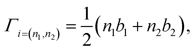
Fig. 2(a) shows the geometry optimized crystal lattice structure of PbCX3 monolayer, where the unit cell has been represented by the shaded region and the Brillouin zone of the hexagonal lattice cell with high symmetry points is shown in Fig. 2(b). The buckling height (δ) and Pb–CX3 bond length (d2) can be measured from side of view of the monolayer in Fig. 2(c).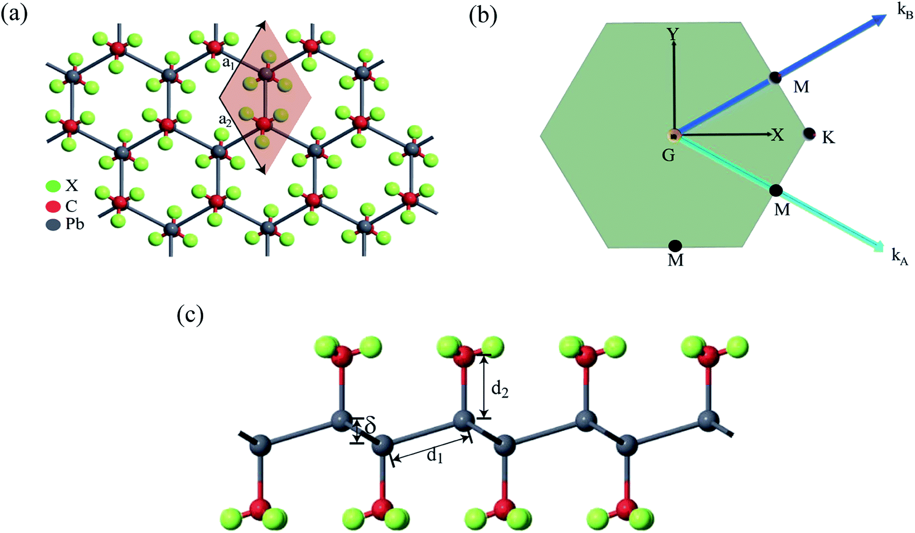 | ||
| Fig. 2 (a) Methyl decorated plumbene monolayer (top view) showing the unit cell with hexagonal crystal lattice, (b) Brillouin zone of the hexagonal crystal lattice with high symmetry points G, M, K, and (c) side view of methyl decorated plumbene monolayer showing the Pb–Pb bond length (d1), Pb–CX3 bond length (d2), buckling height (δ). | ||
The results of geometry optimization and bandstructure calculation of methyl (CH3) and trihalogenomethyl (CX3) decorated plumbene nanosheets are summarized in Table 2. As can be seen from the table, the buckling height (0.8863 Å) of the methyl (CH3) substituted plumbene monolayer is higher compared to that of H-decorated monolayer (0.7781 Å)20 due to more dominant +I inductive effect of (CH3) which assists in effective hybridization of π and σ orbitals.
 topological invariant for different PbCX3 monolayers
| Monolayer | a (Å) | d1 (Å) | d2 (Å) | δ1 (Å) | Eg (SOC) | ΔE (eV per atom) |
|
|---|---|---|---|---|---|---|---|
| Pb | 4.92845 | 3.02 | — | 1.0071 | 0.3229 | — | 0 |
| PbCH3 | 5.07407 | 3.06 | 2.31 | 0.8863 | 0.9818 | −1.3001 | 1 |
| PbCF3 | 5.12554 | 3.06 | 2.37 | 0.7904 | 0.9692 | −2.42002 | 1 |
| PbCCl3 | 5.7454 | 3.34 | 2.40 | 0.406 | 0.841386 | −1.70637 | 1 |
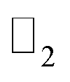
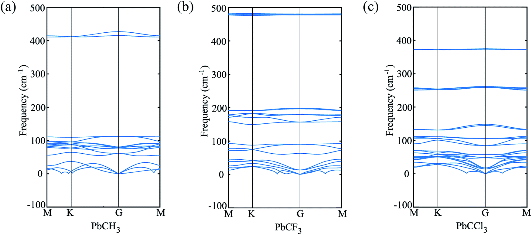
The buckling height suddenly decreases in case of –CCl3 group due to more electronegativity of the group which attracts the π electrons towards it and thus weakening the coupling between π and σ orbitals. The electronic stability of the structures was ensured from their formation energy ΔE using the eqn (1), and the values obtained for PbCH3, PbCF3 and PbCCl3 are −1.3001 eV per atom, −2.42002 eV per atom and −1.70637 eV per atom respectively. The negative formation energy indicates that there will be no phase separation between Pb and CX3 in PbCX3. The thermodynamic stability was ensured from phonon dispersion curves of the decorated structures [Fig. 3]. The presence of no branch in the negative frequency region indicates that methyl, trifluoromethyl and trichloromethyl plumbene would be stable at room temperature. The electronic and thermodynamic stability were also checked from molecular dynamics simulation [Fig. 4]. Fig. 4(a) and (c) show the initial and stable stages, respectively of molecular dynamics for PbCH3 nanoribbon. The nanoribbon is periodic perpendicular to the page. The CH3 groups were placed at a distance of 3.53 Å from the plumbene nanoribbon at the initial step. Fig. 4(b) shows the position of the atoms when the kinetic energy is maximum. In Fig. 4(c), we observe that CH3 groups nicely become attached with the lead atom sites and there is no broken bond at room temperature when stable structure is formed. Fig. 4(d) shows the change of kinetic energy with respect to time for PbCH3 particles. We see that the kinetic energy of the particles initially increases and after forming the bonds, the system energy becomes stable where the particles periodically oscillate without breaking any bond. Simulations were repeated for CF3 and CCl3 groups and similar results were found confirming the stability of all the structures at room temperature. We have also simulated the structural and electronic property of tribromomethyl plumbene (PbCBr3) and triiodomethyl plumbene (PbCI3) monolayers, but due to the lack of any definite stable geometric structure and phase separation between plumbene and (CBr3, CI3), these materials were not further considered for verification of topological properties.
 | ||
| Fig. 3 Phonon dispersion curves showing no branch in the negative frequency region and thermodynamic stability at room temperature. (a) PbCH3 monolayer, (b) PbCF3 monolayer and (c) PbCCl3 monolayer. | ||
 | ||
| Fig. 4 (a) The initial step (time = 0 ps) of molecular dynamics simulation of a PbCH3 nanoribbon. It is periodic perpendicular to the page. (b) The stage of molecular simulation where CH3 particles attain maximum kinetic energy (time = 0.054 ps), (c) the stable structure with no broken bond at room temperature (time = 0.454 ps) and (d) variation of system energy and temperature with respect to time. Red points, labelled as 1, 2 and 3, on the kinetic energy curve correspond to the position of the frames shown in (a), (b) and (c), respectively. | ||
Next, we focus on the bandstructure and partial density of states (PDOS) to observe the effect and origin of spin–orbit coupling. Fig. 5(a) and (b) show the bandstructure of PbCH3 crystal without and with spin–orbit coupling, respectively. The bandgap obtained for PbCH3 taking the spin–orbit coupling into account is 0.9818 eV. The contribution of Pb px,y and Pb pz orbitals to each band of PbCH3 are shown in colored red and green circles from which we see that the main contributions to valence and conduction bands near Fermi level are due to Pb px,y orbitals.
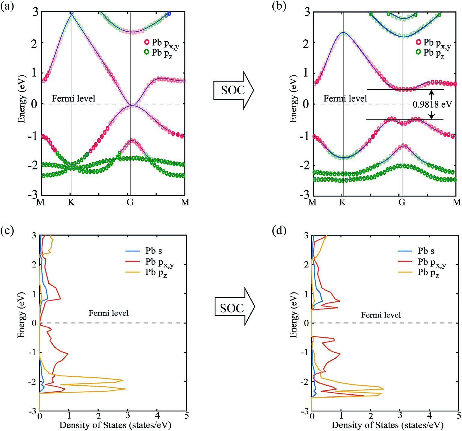 | ||
| Fig. 5 (a) Band structure of the PbCH3 monolayer showing the contribution of Pb px,y and Pb pz orbitals in forming the bands without spin–orbit coupling, (b) band structure of the PbCH3 monolayer with spin–orbit coupling, (c) partial density of states showing the contributions of Pb s, Pb px,y and Pb pz orbitals without spin–orbit coupling (d) partial density of states with spin–orbit coupling. From the figures, it is seen that the major contribution to the bands near to Fermi level is due to Pb px,y orbitals. | ||
Observing the contribution of orbitals from partial density of states (PDOS) in Fig. 5(c) and (d), we see that when spin–orbit coupling is introduced, the degeneracy of Pb px,y orbitals causes the bandgap opening near Fermi level. The lower bands are due to the contribution from Pb pz orbital as shown in the Fig. 5(c) and (d).
Similar phenomena of the bandgap opening occurs for PbCF3 and PbCCl3 monolayer crystals and the bandgaps obtained for PbCF3 and PbCCl3 with spin–orbit coupling are 0.9692 eV and 0.8414 eV, respectively as shown in Fig. 6. These range of bandgap are enough for room and high temperature application, as it is much higher than thermal energy of electron at room temperature (0.0259 eV).
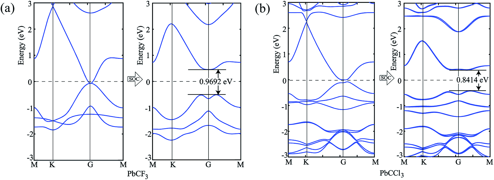 | ||
| Fig. 6 (a) Band structure of PbCF3 monolayer without and with spin–orbit coupling, (b) bandstructure of PbCCl3 monolayer without and with spin–orbit coupling. | ||
To verify our simulation method, the electronic structures of PbCH3 and PbCF3 monolayers were calculated employing HSE06 (ref. 47) functional. The bandstructures calculated for PbCH3 and PbCF3 monolayers without and with spin–orbit coupling are shown in Fig. 7. The bandgaps obtained for PbCH3 and PbCF3 monolayers using this method are found to be 1.2623 eV and 1.2498 eV respectively. As GGA-PBE is known to underestimate the bandgaps, the bandstructures obtained from HSE06 functional are consistent with GGA-PBE.
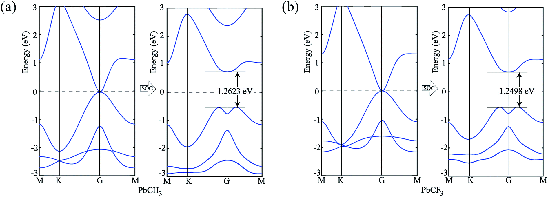 | ||
| Fig. 7 Bandstructures without and with spin–orbit coupling employing HSE06 functional. (a) PbCH3 monolayer and (b) PbCF3 monolayer. | ||
The effect of spin–orbit coupling leads to formation of edge states and these edges will have to be topologically protected for protection against backscattering. The robustness of these edge states against backscattering is determined from topologically invariant property. Thus, to find the robustness of the edge states we have calculated the topological  invariant of the each monolayer. For example, if we consider PbCH3, there are 4 valence electrons in the outer shell of Pb, C and 1 valence electron in hydrogen. Hence, the total number of valence electrons in each crystal lattice shell is 2 × (4 + 4 + 3 × 1) = 22. By calculating the 〈ψi,n|Θ|ψi,n〉 at the 2mth occupied band, we found the symmetry function δi at each symmetry points G(0,0), M(0,0.5), M(0.5,0) and M(0.5,0.5). As 〈ψi,n|Θ|ψi,n〉 at the 2m − 1th and 2mth bands is same due to spin degeneracy, the product of
 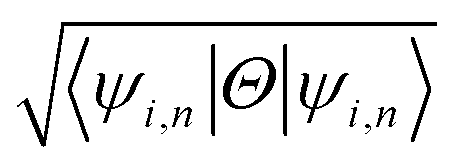 at the 2m − 1th and 2mth bands
 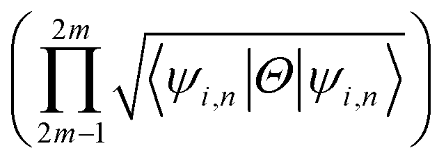 is essentially the same as the value of 〈ψi,n|Θ|ψi,n〉 at the 2mth band. Then, the topological invariant is calculated using eqn (4), as shown in Table 3 and the
  topological invariant with ν = 1 indicates the topological nontriviality.
| Γi | 〈ψi,n|Θ|ψi,n〉 of 2mth occupied band | δi |
|---|---|---|
| (0,0) | − − + + − + − + − + − | + |
| (0.5,0) | + − + − + − + − + − + | − |
| (0,0.5) | + − + − + − + − + − + | − |
| (0.5,0.5) | + − + − + − + − − + + | − |
| PbCH3 |  topological invariant topological invariant |
ν = 1 |
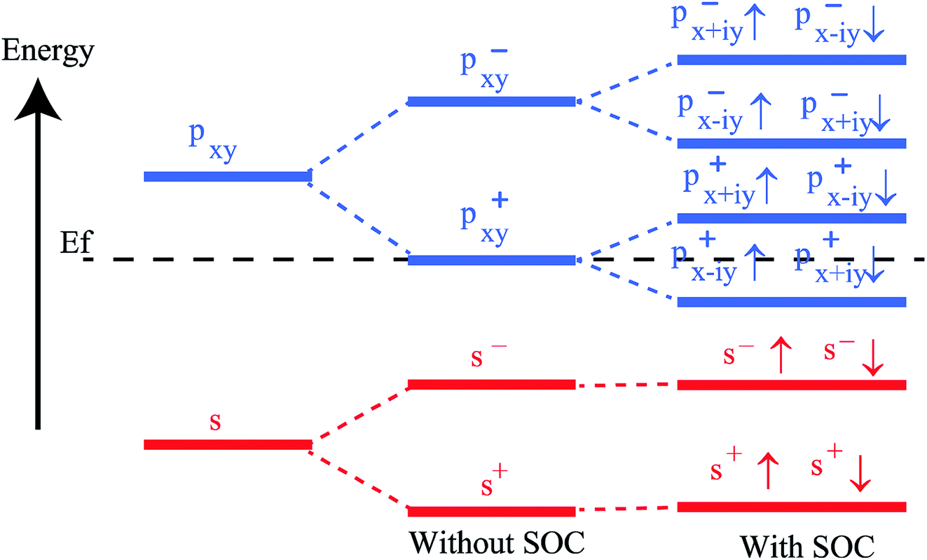
To get a clear understanding of the origin of bandgap and topological nontriviality, we have presented the methodical band evolution at G point for PbCH3 in Fig. 8. Analyzing the bandstructure and partial density of states in Fig. 5, we have done an orbital analysis to investigate the origin of topological characteristics. From partial density of states (PDOS) of PbCH3 in Fig. 5(c) and (d), we see that the Pb s and Pb px,y orbitals dominate the valence and conduction bands near the Fermi level. When chemical bonding is formed between Pb–Pb atoms, then effect of crystal field splitting creates bonding states and anti-bonding states for the s and px,y orbitals, which we have denoted with |s,±〉 and |px,y,±〉, where + and − represent the parities of the corresponding state, respectively. As displayed in Fig. 8, the bands near the Fermi level are due to |px,y,±〉 in absence of spin–orbit coupling (SOC). When the spin–orbit coupling is included in the calculation, the degeneracy of the level splits into |px,y,±3/2〉 states with a total angular momentum j = 3/2 and |px,y,±1/2〉 with a total angular momentum j = 1/2, creating an energy gap at the G point. Similar analysis can be done and same conclusion can be drawn for PbCCl3 and PbCF3. The presence of edge states and topological invariant can be clearly observed if we construct a semi-infinite PbCH3 sheet and investigate its bandstructure.
 | ||
| Fig. 8 The orbital analysis of PbCH3 at G(0,0) point, which shows that contribution of s and px,y atomic orbitals to bands near Fermi level. The bandstructure formation is mainly due to crystal field splitting and spin–orbit coupling. | ||
Thus, we construct a semi-infinite PbCH3 sheet (nanoribbon) of width 160 Å which is sufficient to get rid of the interaction between edge states39 (Fig. 9(a)). The nanoribbon has edges in the zigzag direction and the dangling bonds at the edges were passivated by hydrogen atoms. Fig. 9(b) shows the corresponding bandstructure of PbCH3 nanoribbon indicating topological invariant 1  from the odd number of band crossing the Fermi level. The Fermi velocity obtained for electrons in PbCH3 nanoribbon is 7.38 × 10⁵ m s−1 as calculated from Fig. 9(b) using the formula E = ℏvfk suggesting its possible application in high speed electronics. Same phenomena were observed in PbCF3 and PbCCl3 nanoribbons and the corresponding bandstructures are given in Fig. 9(c) and (d).
 | ||
Fig. 9 (a) PbCH3 nanoribbon along zigzag direction. The dangling bond at the edge are passivated by hydrogen. The blue and red colors arrows represent the edge states due to up and down spin respectively. (b) Bandstructure of zigzag PbCH3 nanoribbon showing odd number of band passing through Fermi level which proves the  topological invariant of 1. The red color band corresponds to the bands due to edge states. (c) Bandstructure of zigzag PbCF3 nanoribbon. (d) Bandstructure of zigzag PbCCl3 nanoribbon. topological invariant of 1. The red color band corresponds to the bands due to edge states. (c) Bandstructure of zigzag PbCF3 nanoribbon. (d) Bandstructure of zigzag PbCCl3 nanoribbon. | ||
Lastly, in order to investigate the stability of the materials and change of properties with change of strain (±4%), we have shown the variation of bandgap and formation energy versus strain. From Fig. 10(a), we see that the bandgap of PbCH3 decreases gradually with the increase of strain and increases upto compression strain of 4%. The formation energies in the negative region, shown by Fig. 10(b), ensures the electronic stability of the materials under strain. The bandgap vs. strain curve of PbCF3 is almost linear in the total range of strain. It has been previously discussed that bandgap opens mainly due to p–p orbital splitting with spin–orbit coupling. Thus, the reason behind the strain-dependent variation of bandgaps can be found from orbital analysis. Fig. 10(c) shows that the p–p orbital splitting decreases with compressive strain and increases with the increase of tensile strain, and the bandgaps follow the trend accordingly. We have not applied strain more than 4% because beyond that it leads to structural deformation. Thus, changing the strain in methyl and trihalogenomethyl decorated plumbene monolayer may produce topological insulators with much higher bandgap.
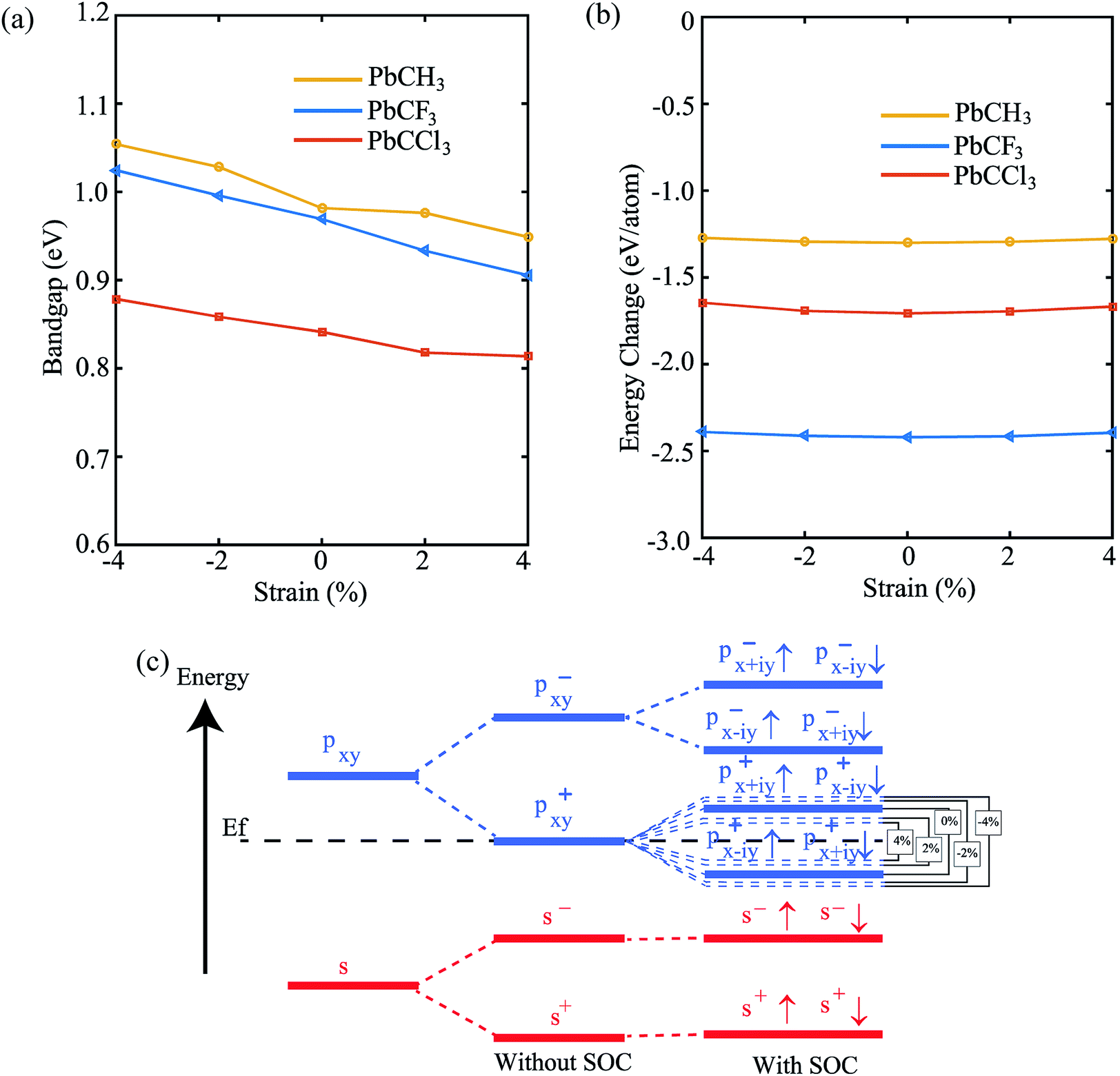 | ||
| Fig. 10 (a) The change of bandgap (Eg) with spin–orbit coupling (SOC) with change of strain, (b) the change of formation energy ΔE with strain. The negative values of formation energies ensure electronic stability. (c) The orbital analysis of PbCH3 at G(0,0) point for different percentages of strain, which shows that contribution of s and px,y atomic orbitals to bands near Fermi level. The amount of splitting in p–p orbitals is changed as shown by the dotted lines. | ||
Conclusions
We have predicted a new family of methyl and trihalogenomethyl decorated plumbene monolayer, as large band gap quantum spin Hall insulators, showing excellent topological property at room temperature. Orbital analysis shows that the band gap opening is mainly due to p–p band splitting caused by spin–orbit coupling. The topological invariant confirms the robustness of edge states against backscattering that is protected by time-reversal symmetry. The presence of edge states in the bandstructure obtained by simulating nanoribbons further confirms its edge states and topological nontriviality. We have also seen its structural stability against externally applied strain which enhances the possibility of obtaining topological insulators with higher bandgaps using strain. These findings demonstrate that the methyl and trihalogenomethyl decorated Pb films may be good QSH platforms for the design of topological electronic devices, spintronics and dissipationless electronics.
Conflicts of interest
There are no conflicts to declare.Notes and references
- M. Z. Hasan and C. L. Kane, Rev. Mod. Phys., 2010, 82, 3045 CrossRef CAS.
- R. J. Cava, H. Ji, M. K. Fuccillo, Q. D. Gibson and Y. S. Hor, J. Mater. Chem. C, 2013, 1, 3176–3189 RSC.
- C. L. Kane and E. J. Mele, Phys. Rev. Lett., 2005, 95, 146802 CrossRef CAS PubMed.
- H. Zhao, W.-x. Ji, C.-w. Zhang, P. Li, S.-f. Zhang, F. Li, P.-j. Wang, S.-s. Li and S.-s. Yan, J. Mater. Chem. C, 2017, 5, 2656–2661 RSC.
- M. König, S. Wiedmann, C. Brüne, A. Roth, H. Buhmann, L. W. Molenkamp, X.-L. Qi and S.-C. Zhang, Science, 2007, 318, 766–770 CrossRef PubMed.
- I. Knez, R.-R. Du and G. Sullivan, Phys. Rev. Lett., 2011, 107, 136603 CrossRef PubMed.
- C. L. Kane and E. J. Mele, Phys. Rev. Lett., 2005, 95, 226801 CrossRef CAS PubMed.
- Y. Yao, F. Ye, X.-L. Qi, S.-C. Zhang and Z. Fang, Phys. Rev. B: Condens. Matter Mater. Phys., 2007, 75, 041401 CrossRef.
- L. Matthes, O. Pulci and F. Bechstedt, J. Phys.: Condens. Matter, 2013, 25, 395305 CrossRef PubMed.
- Y.-p. Wang, W.-x. Ji, C.-w. Zhang, P. Li, S.-f. Zhang, P.-j. Wang, S.-s. Li and S.-s. Yan, Appl. Phys. Lett., 2017, 110, 213101 CrossRef.
- S.-j. Zhang, C.-w. Zhang, S.-f. Zhang, W.-x. Ji, P. Li, P.-j. Wang, S.-s. Li and S.-s. Yan, Phys. Rev. B: Condens. Matter Mater. Phys., 2017, 96, 205433 CrossRef.
- W. Yu, C.-Y. Niu, Z. Zhu, X. Cai, L. Zhang, S. Bai, R. Zhao and Y. Jia, RSC Adv., 2017, 7, 27816–27822 RSC.
- S. Balendhran, S. Walia, H. Nili, S. Sriram and M. Bhaskaran, Small, 2015, 11, 640–652 CrossRef CAS PubMed.
- S. Z. Butler, S. M. Hollen, L. Cao, Y. Cui, J. A. Gupta, H. R. Gutiérrez, T. F. Heinz, S. S. Hong, J. Huang and A. F. Ismach, ACS Nano, 2013, 7, 2898–2926 CrossRef CAS PubMed.
- X.-L. Yu and J. Wu, Phys. Chem. Chem. Phys., 2018, 20, 2296–2307 RSC.
- M.-h. Zhang, C.-w. Zhang, P.-j. Wang and S.-s. Li, Nanoscale, 2018, 10, 20226–20233 RSC.
- Y.-z. Jia, W.-x. Ji, C.-w. Zhang, S.-f. Zhang, P. Li and P.-j. Wang, RSC Adv., 2017, 7, 11636–11643 RSC.
- C.-C. Liu, W. Feng and Y. Yao, Phys. Rev. Lett., 2011, 107, 076802 CrossRef PubMed.
- C.-C. Liu, H. Jiang and Y. Yao, Phys. Rev. B: Condens. Matter Mater. Phys., 2011, 84, 195430 CrossRef.
- H. Zhao, C.-w. Zhang, W.-x. Ji, R.-w. Zhang, S.-s. Li, S.-s. Yan, B.-m. Zhang, P. Li and P.-j. Wang, Sci. Rep., 2016, 6, 20152 CrossRef CAS PubMed.
- Y. Lu, D. Zhou, T. Wang, S. A. Yang and J. Jiang, Sci. Rep., 2016, 6, 21723 CrossRef CAS PubMed.
- Y. Xu, B. Yan, H.-J. Zhang, J. Wang, G. Xu, P. Tang, W. Duan and S.-C. Zhang, Phys. Rev. Lett., 2013, 111, 136804 CrossRef PubMed.
- R.-w. Zhang, W.-x. Ji, C.-w. Zhang, S.-s. Li, P. Li and P.-j. Wang, J. Mater. Chem. C, 2016, 4, 2088–2094 RSC.
- M. Krawiec, J. Phys.: Condens. Matter, 2018, 30, 233003 CrossRef PubMed.
- H. Zhao, W.-x. Ji, C.-w. Zhang, P. Li, F. Li, P.-j. Wang and R.-w. Zhang, Phys. Chem. Chem. Phys., 2016, 18, 31862–31868 RSC.
- Z. Ni, Q. Liu, K. Tang, J. Zheng, J. Zhou, R. Qin, Z. Gao, D. Yu and J. Lu, Nano Lett., 2011, 12, 113–118 CrossRef PubMed.
- S. Nigam, S. K. Gupta, C. Majumder and R. Pandey, Phys. Chem. Chem. Phys., 2015, 17, 11324–11328 RSC.
- N. Gao, J. Li and Q. Jiang, Chem. Phys. Lett., 2014, 592, 222–226 CrossRef CAS.
- W.-W. Yan, X.-F. Li, X.-H. Zhang, X. Cao and M. Deng, J. Mater. Chem. C, 2019, 7, 6241–6245 RSC.
- H. Sahin and F. M. Peeters, Phys. Rev. B: Condens. Matter Mater. Phys., 2013, 87, 085423 CrossRef.
- M. Ezawa, New J. Phys., 2012, 14, 033003 CrossRef.
- J. Padilha, R. Pontes, T. Schmidt, R. Miwa and A. Fazzio, Sci. Rep., 2016, 6, 26123 CrossRef CAS PubMed.
- J. Wu, L. Xie, Y. Li, H. Wang, Y. Ouyang, J. Guo and H. Dai, J. Am. Chem. Soc., 2011, 133, 19668–19671 CrossRef CAS PubMed.
- K. N. Kim, V. P. Pham and G. Y. Yeom, ECS J. Solid State Sci. Technol., 2015, 4, N5095–N5097 CrossRef CAS.
- L. Wu, K. Gu and Q. Li, Appl. Surf. Sci., 2019, 484, 1208–1213 CrossRef CAS.
- R.-W. Zhang, C.-W. Zhang, W.-X. Ji, S.-S. Li, S.-J. Hu, S.-S. Yan, P. Li, P.-J. Wang and F. Li, New J. Phys., 2015, 17, 083036 CrossRef.
- S.-s. Li, W.-x. Ji, C.-w. Zhang, S.-j. Hu, P. Li, P.-j. Wang, B.-m. Zhang and C.-l. Cao, Sci. Rep., 2016, 6, 23242 CrossRef CAS PubMed.
- Y. Ma, Y. Dai, W. Wei, B. Huang and M.-H. Whangbo, Sci. Rep., 2014, 4, 7297 CrossRef CAS PubMed.
- C.-C. Ren, W.-X. Ji, S.-F. Zhang, C.-W. Zhang, P. Li and P.-J. Wang, Nanomaterials, 2018, 8, 698 CrossRef PubMed.
- A. T. Version, 2017, accessed on 25 September 2018 Search PubMed.
- R. H. Byrd, P. Lu, J. Nocedal and C. Zhu, SIAM J. Sci. Comput., 1995, 16, 1190–1208 CrossRef.
- J. P. Perdew, K. Burke and M. Ernzerhof, Phys. Rev. Lett., 1996, 77, 3865 CrossRef CAS PubMed.
- H. J. Monkhorst and J. D. Pack, Phys. Rev. B: Solid State, 1976, 13, 5188 CrossRef.
- K. Stokbro, B. K. Nikolic and A. M. Bratkovsky, Computing noncollinear spins and spin torque in ATK from QuantumWise A/S, QuantumATK Technical Note, 2013, pp. 1–5, available at https://docs.quantumatk.com/_downloads/technote.pdf, accessed 16 December 2019 Search PubMed.
- K. F. Garrity, J. W. Bennett, K. M. Rabe and D. Vanderbilt, Comput. Mater. Sci., 2014, 81, 446–452 CrossRef CAS.
- L. Fu and C. L. Kane, Phys. Rev. B: Condens. Matter Mater. Phys., 2007, 76, 045302 CrossRef.
- J. Heyd, G. E. Scuseria and M. Ernzerhof, J. Chem. Phys., 2003, 118, 8207–8215 CrossRef CAS.
| This journal is © The Royal Society of Chemistry 2019 |