
 Open Access Article
 This Open Access Article is licensed under a Creative Commons Attribution-Non Commercial 3.0 Unported Licence
Low-threshold room-temperature continuous-wave optical lasing of single-crystalline perovskite in a distributed reflector microcavity†
Cheng Tian ,
Tong guo,
Shiqi Zhao,
Wenhao Zhai,
Chaoyang Ge and
Guangzhao Ran*
,
Tong guo,
Shiqi Zhao,
Wenhao Zhai,
Chaoyang Ge and
Guangzhao Ran*
State Key Laboratory for Artificial Microstructure and Mesoscopic Physics, School of Physics, Peking University, Beijing 100871, China. E-mail: rangz@pku.edu.cn
First published on 5th November 2019
Abstract
Organic–inorganic halide perovskites have achieved remarkable success in various optoelectronic devices. A high-quality CH3NH3PbBr3 single-crystalline thin film has been directly grown in a micrometer gap between a pair of distributed reflectors with over 99.9% reflectivity, which naturally form a vertical cavity surface-emitting laser device with a single mode or several modes. The single-crystalline perovskite has an exciton lifetime of 426 ns and evidence of the exciton–photon coupling is observed. At room temperature and under continuous-wave optical pumping conditions, this device lases at a threshold of 34 mW cm−2 in the green gap. The extremely low lasing threshold suggests that polariton lasing may occur in the strongly confined optical cavity comprising the high-quality single-crystalline perovskite.
1. Introduction
Low-cost solution-synthesized organic–inorganic halide perovskites have increasingly become ideal materials for solar cells, light-emitting diodes, lasers, etc. in the past few decades. Recently, perovskite solar cells have achieved a certified efficiency approaching that of the single-crystalline silicon cells.1 Numerous optically pumped perovskite lasers have been reported based on the as-grown micro/nano-structures2–6 and polycrystalline films in vertical microcavities.7–10 Single-crystalline materials generally possess better optoelectronic properties compared to polycrystalline and amorphous ones. Perovskite single-crystalline bulks can be grown in inch size but they are difficult to directly use in laser fabrication until sliced into thin wafers. To date, spin-coated perovskite polycrystalline films are mostly applied in conventional optoelectronic devices, including vertical cavity surface-emitting lasers (VCSEL).7,9,10 A perovskite film which is around one micrometer thick is needed in a VCSEL according to the resonance conditions.Acquiring a single crystal with high quality and appropriate thickness simultaneously is vital for a high performance of perovskite optoelectronic devices. The space-confined method for fabricating single-crystalline perovskite thin films11 can satisfy the above requirements and maintain some excellent properties of single-crystalline bulks as well, such as high mobility, low trap density, long carrier lifetime and diffusion length. Based on this method, the perovskite solar cells have exceeded 21% in power conversion efficiency,12 perovskite photodetectors have achieved a 100-photon level detection limit13 and perovskite field-effect mobility has reached 4.7 cm2 (V−1 s−1) at room temperature.14 However, well performing laser devices of perovskite single-crystalline thin films have been reported rarely15 and so have the continuous-wave (CW) ones.
In this work, we have in situ grown single-crystalline CH3NH3PbBr3 (MAPbBr3) thin films between a pair of distributed reflectors (DBR) cavity to construct a VCSEL. The conventional method for a DBR VCSEL with single-crystalline perovskite usually involves transferring the single-crystalline perovskite thin film on a DBR substrate and then covering or depositing the top DBR. Whereas transferring the perovskite film or covering the top DBR possibly leaves an air gap with an uncontrollable thickness, causing an uncontrollable cavity length and optical loss. Additionally, depositing top DBR requires the time-consuming ultrahigh vacuum technology and may damage the underlying perovskite active layer, lowering photoluminescence (PL) quantum yield. On the other hand, with reduced dimensionality, exciton–photon interaction can occur in perovskites, giving the pathway to obtain highly efficient optical devices. In situ grown microcavity device lases at room temperature and under continuous-wave condition with an extremely lasing threshold.
2. Experiment
MAPbBr3 single-crystalline thin films were grown by using the space-confinement method between quartz and DBR substrates. The precursor solution was prepared by dissolving CH3NH3Br and PbBr2 with 1![[thin space (1/6-em)]](https://www.rsc.org/images/entities/char_2009.gif) :1 molar ratio into anhydrous dimethylformamide (DMF) for a molar concentration of 1 mol L−1 at first. The solution was then stirred with a magnetic rotor overnight until it became clear and transparent. The solution was filtered by polytetra-fluoroethylene filter membrane with 0.22 μm apertures to remove the residue. Then several microliters of perovskite precursor solution were dropped onto the surface of a clean substrate (typically 12 × 12 mm2) and another piece of substrate was put on the top to form a thin gap. The samples were left to grow at constant 25 °C for over 24 hours and then transferred to a vacuum desiccator to remove the residual solvent for a week. As the solvent evaporated, the crystals grew along the parallel direction of the substrate and in the confined gap. Finally, MAPbBr3 single-crystalline thin films have been directly grown in the gaps between the paired substrates.
:1 molar ratio into anhydrous dimethylformamide (DMF) for a molar concentration of 1 mol L−1 at first. The solution was then stirred with a magnetic rotor overnight until it became clear and transparent. The solution was filtered by polytetra-fluoroethylene filter membrane with 0.22 μm apertures to remove the residue. Then several microliters of perovskite precursor solution were dropped onto the surface of a clean substrate (typically 12 × 12 mm2) and another piece of substrate was put on the top to form a thin gap. The samples were left to grow at constant 25 °C for over 24 hours and then transferred to a vacuum desiccator to remove the residual solvent for a week. As the solvent evaporated, the crystals grew along the parallel direction of the substrate and in the confined gap. Finally, MAPbBr3 single-crystalline thin films have been directly grown in the gaps between the paired substrates.
3. Results and discussion
Fig. 1(a) shows the scanning electron microscope (SEM) image of the grown perovskite single-crystalline thin film, which exhibits a smooth surface and distinct edges and corners. PL lifetime measurement is performed and depicted in Fig. 1(b) in order to study the carrier kinetics. The PL decay curve can be fitted perfectly by a double exponential function. The fast component (τ1 = 11 ns) is believed to originate from recombination in the crystal surface with high trap density, while the slow one (426 ns) is related to the bulk recombination. The long PL lifetime, which is comparable to the best reported value of single-crystalline bulks,16 indicates grown high-quality single crystal thin films. The X-ray diffraction patterns in Fig. 1(c) indicate that the film has a single-crystalline structure and the crystal orientation in the direction perpendicular to the substrate is (001). The full width at half maximum (FWHM) of the (001) peak is only 0.06°, close to that reported previously.13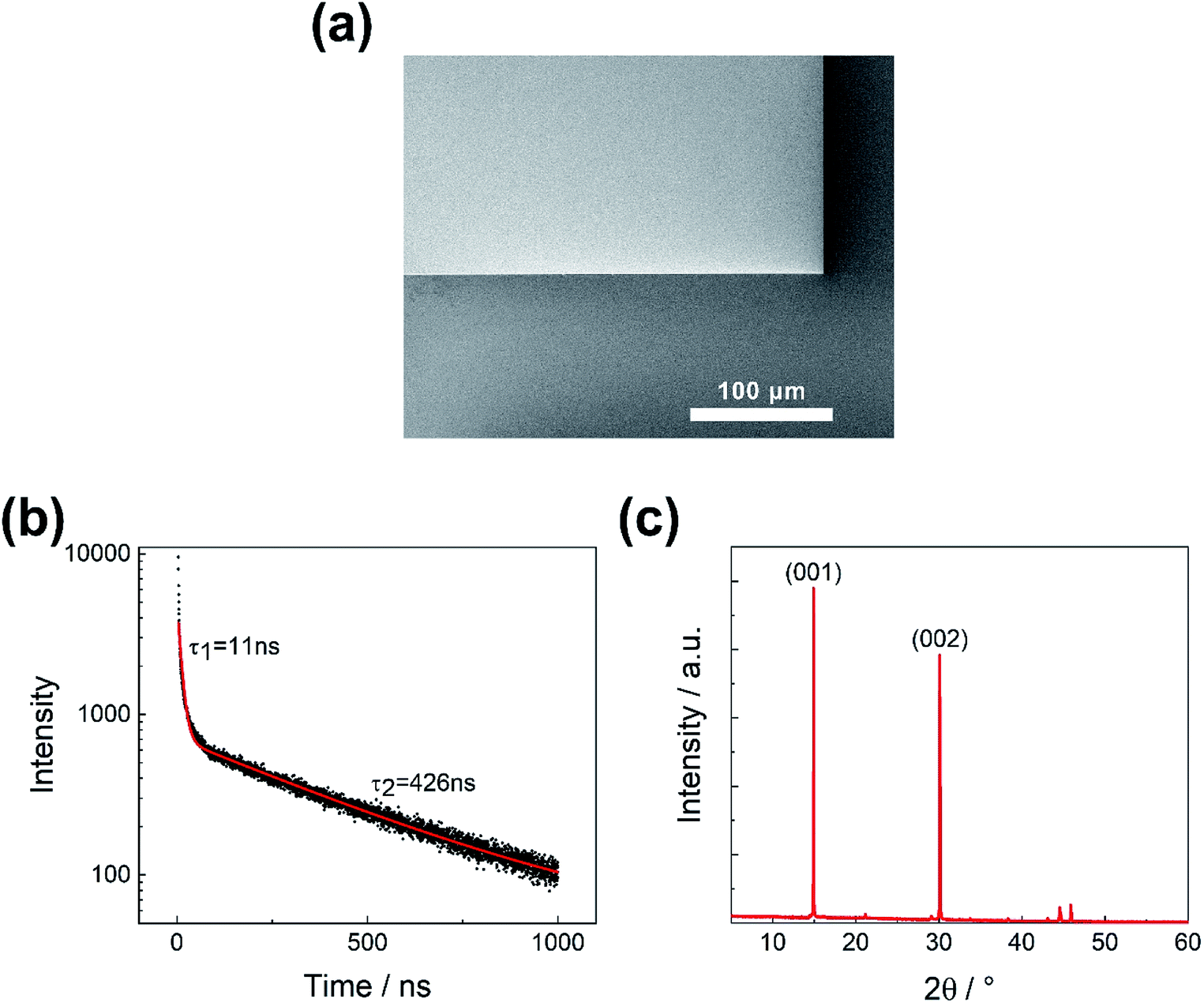 | ||
| Fig. 1 (a) The SEM image of the micron-thickness MAPbBr3 single-crystalline thin film with the scale bar of 100 μm. (b) PL lifetime curve of the MAPbBr3 thin film (black dotted line) and a double exponential function fitting curve of the data (red solid line). (c) The X-ray diffraction patterns of the MAPbBr3 film. | ||
The PL spectrum of the single-crystalline MAPbBr3 thin film grown in-between two slices of quartz was measured. Although the interfaces between quartz slices and the MAPbBr3 film have very weak reflection, the PL spectrum exhibits some interference patterns. To our surprise, when the quartz superstrate was removed, sharp peaks appear in the spectrum of the MAPbBr3 film in free space, as shown in the top curve of Fig. 2(a). The optical longitudinal modes of the active cavity consisted of the MAPbBr3 film have a relationship mλpeak = 2neffh, where h = 2.2 μm stands for the thickness of the film, measured by cross-section SEM. The spectrum presents six pattern peaks, but the energy intervals of these peaks are not uniform and neither the wavelengths of them are consistent with this relationship. So, energy–wavevector (E–k) dispersion was fitted with a two-coupled oscillator (exciton versus photon) model.17,18 Fig. 2(c) shows the data of peak positions and the dispersion curve from the model, which will be discussed in depth in the following sections. The detailed numerical calculations are supplied in ESI.†
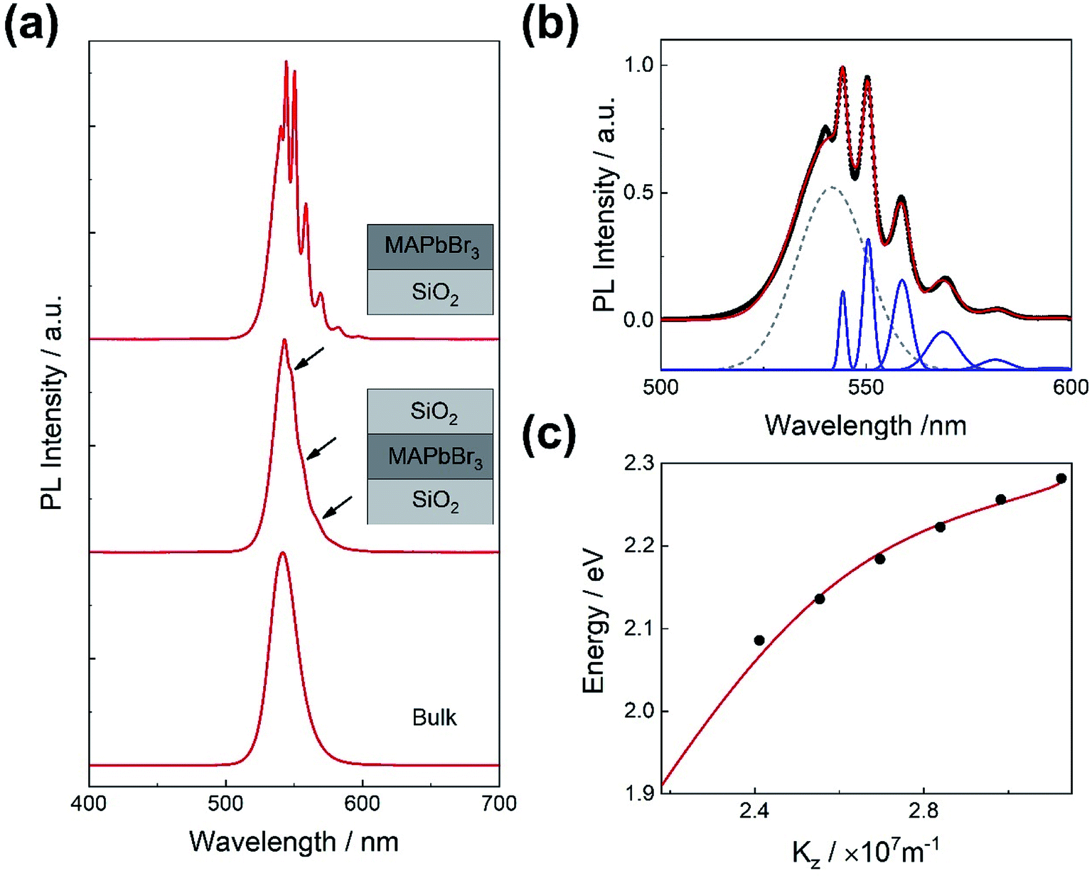 | ||
| Fig. 2 (a) The bottom curve stands for the PL spectrum of a centimeter-sized bulk of MAPbBr3. The middle curve stands for a film in-between quartz substrates with weak patterns pointed by the arrows due to interference effect. And the top curve stands for a film only on a quartz substrate with obvious modes because of the higher difference of the refractive index between the film and air. (b) The PL spectra and the fitted curve of the MAPbBr3 single-crystalline film on a quartz substrate without a superstrate from 500 nm to 600 nm. The black dots stand for experimental data, the gray dashed curve stands for the spontaneous emission background spectrum, the blue curves stand for peaks of the strong patterns and the red curve stands for the fitted curve of the dots, summing up from the data of gray and blue curves. (c) The dispersion curve of the MAPbBr3 film. The black data dots indicate peaks which have been placed in wave vector space at integer values of π/h with h = 2.2 μm for the film thickness. The red solid line shows the results of numerical calculations of a two-coupled oscillator model for the fundamental mode. | ||
The optical confinement was enhanced by replacing quartz with a pair of DBR mirrors as shown in Fig. 3(a), which form the structure of a perovskite VCSEL. The commercially available DBR substrates, consisted of 13.5 pairs of alternating TiO2/SiO2, have over 99.9% reflectivity near the emitting peak wavelength of MAPbBr3 in free space. Fig. 3(b) is the optical image in the dark field mode, as the visible light hardly passes through the DBR substrates. The distinct edges and corners can also be observed from the image. The thickness of thin films can be controlled by simply applying pressure on the superstrates. Considering the fact that films thinner than 100 nm cannot support any cavity mode and that the thick films absorb over 99% incident light in a 400 nm distance, a film with the thickness around 1 μm that can support several modes was chosen to grow between DBR substrates.
 | ||
| Fig. 3 (a) The schematic diagram of the structure of perovskite VCSEL. The yellow wafers stand for single-crystalline perovskite thin films. (b) The dark field optical image of the MAPbBr3 film between two DBR substrates with the scale bar of 200 μm. | ||
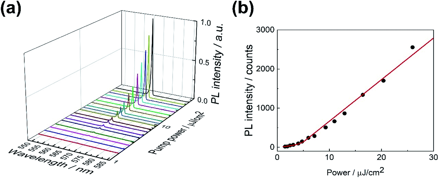
A CW semiconductor laser (405 nm) was adopted to pump the perovskite laser devices at room temperature in ambient air and the results and analysis are shown in Fig. 4. Fig. 4(a) shows the excitation-fluence dependent PL spectra collected from the surface of the DBR/perovskite/DBR samples. As the fluence power increases, a sharp peak at nearly 565 nm appears with two side peaks. This peak increases nonlinearly accompanied with linewidth narrowing, and the final FWHM reaches 0.8 nm. Fig. 4(b) compares the lasing spectrum under the highest pump fluence and the reflection spectrum of the designed DBR, witnessing that the peak sits near the center of the high reflection zone. Fig. 4(c) shows two linear regions and a turn at around 34 mW cm−2. To obtain a clearer illustration, Fig. 4(d) replots the output intensity versus input pump fluence (L–L curve) data in a logarithmic coordinate system, which is characterized by a visible S-shaped kink between the two parallel linear regions. The data were fitted with a classical rate equation analysis7 and obtained the spontaneous emission factor β ∼ 0.08, i.e., the fraction of spontaneous emission coupled into the lasing mode. The fitting curves with β ∼ 0.5, 1 and the same other parameters are also plotted in the black solid line for comparison. Detailed fitting process and parameter selection are provided in ESI.† Two other much weaker side peaks are at 547 and 591 nm, the analysis of which are provided in ESI.† According to the intervals of these three modes, the thickness of the perovskite film is estimated to be 1.36 μm, close to the result measured by SEM and consistent to the growth condition.
 | ||
| Fig. 4 (a) PL spectra evolution under different pump fluences. (b) The spectrum under the highest pump fluence compared to the reflection spectrum of DBR. Spectral coherent lasing peak at 565 nm with an FWHM of 0.8 nm is observed. (c) The L–L curve of 565 nm peak in a natural coordinate system. The red solid lines are the fitting curve from a rate equation model. Two linear regimes can be distinguished, crossed from where the arrow points. (d) The intensity and FWHM of 565 nm peak change along with increasing pump fluences in a logarithmic coordinate system. The red lines are the fitting curve with β ∼ 0.08, 0.5, 1. There is a kink between the two linear regimes of spontaneous emission which gives the threshold energy density of about 34 mW cm−2. | ||
To examine the operation performance under the pulsed pumping condition, the pump source was changed to a nanosecond pulsed laser (355 nm, 8.0 ns pulse width, 1.0 kHz). As shown in Fig. 5(a), a single mode at 567 nm is obtained at room temperature in ambient air as well. The FWHM is 0.7 nm at the highest pump fluence. Fig. 5(b) plots the L–L data in a natural coordinate system. Two linear regimes can be distinguished. There is a turn between the two linear regimes of spontaneous emission which gives the threshold energy density of about 4 μJ cm−2.
 | ||
| Fig. 5 (a) PL spectra (550–585 nm) evolution under different pump fluences. Spectral coherent single-mode lasing peak at 567 nm with an FWHM of 0.7 nm is observed. (b) The L–L curve of the peak in a natural coordinate system. Two linear regimes can be distinguished. There is a turn between the two linear regimes of spontaneous emission which gives the threshold energy density of about 4 μJ cm−2. | ||
Table 1 lists the laser thresholds for the external DBR resonant cavity lasers and all kinds of CW perovskite lasers reported in the references and this work. The threshold pumped by a nanosecond pulsed laser of this work is much smaller than those listed in Table 1 and comparable to those pumped by femtosecond pulsed lasers. Moreover, the CW lasing threshold of this work is three orders of magnitude smaller than those listed in Table 1.
| Material | Morphologya | Pump source | Threshold | Cavity | T/K | Ref. |
|---|---|---|---|---|---|---|
| a QD for quantum dots; NW for nanowire; SC-TF for single-crystalline thin film.b RT for room temperature. | ||||||
| MAPbI3 | Thin film | 532 nm/340 fs | 7.6 μJ cm−2 | DBR | RTb | 7 |
| 532 nm/5 ns | 114 μJ cm−2 | |||||
| CsPbBr3 | QD | 400 nm/100 fs | 11 μJ cm−2 | DBR | RT | 9 |
| 400 nm/5 ns | 900 μJ cm−2 | |||||
| CsPbBr3 | QD | 400 nm/50 fs | 0.39 μJ cm−2 | DBR | RT | 8 |
| 355 nm/5 ns | 98 μJ cm−2 | |||||
| MAPbBr3 | SC-TF | 397 nm/200 fs | 26 μJ cm−2 | DBR | RT | 15 |
| FAPbBr3 | Thin film | 355 nm/340 fs | 18.3 μJ cm−2 | DBR | RT | 10 |
| CsPbCl3 | Nanoplatelet | 375 nm/100 fs | 12 μJ cm−2 | DBR | RT | 19 |
| MAPbBr3 | SC-TF | 355 nm/8 ns | 4 μJ cm−2 | DBR | RT | This work |
| MAPbI3 | Thin film | 455 nm/CW | 17 kW cm−2 | DFB | 102 K | 20 |
| CsPbBr3 | NW | 450 nm/CW | 6 kW cm−2 | FP | 77 K | 21 |
| MAPbI3 | Thin film | 355 nm/CW | 15 W cm−2 | DFB | RT | 22 |
| MAPbBr3 | QD | 405 nm/CW | 15 W cm−2 | DFB | RT | 23 |
| MAPbI3 | 24 W cm−2 | |||||
| MAPbCl3 | 58 W cm−2 | |||||
| MAPbBr3 | SC-TF | 405 nm/CW | 34 mW cm−2 | DBR | RT | This work |
The low lasing thresholds are first attributed to the high quality of both perovskite crystal and the microcavity. The single-crystalline perovskite films have a longer exciton lifetime (426 ns), therefore resulting a higher PL quantum yield than other lasers consisted of spin-coated perovskite films in Table 1. The in situ growth between the substrates guarantees that gain medium and highly reflective DBR mirrors form close contact, and the precisely designed DBR mirrors have over 99.9% reflection. Both of them reduce the loss in the cavity and the mirrors. Moreover, the space-confined fabrication method of DBR perovskite lasers guarantees that the grown perovskite single-crystalline film remains intact and uniform because the grating reflectors and gain medium are independent from each other. As contrast, CW lasers built in DFB cavities listed in Table 1 require perovskite materials to grow into submicron periodic shapes, causing larger scattering loss and nonradiative recombination.
More fundamentally, the extremely low threshold pumped by CW laser suggests that an exciton–photon polariton lasing might occur. The high-quality bromide perovskite single crystals are believed to have large exciton binding energy, which reaches 71 meV theoretically and 40−150 meV measured by optical absorption or temperature dependent PL,24,25 comparable to the room temperature thermal energy of kBT = 26 meV. When perovskite materials are used as the gain medium, evident exciton effect can be observed even at room temperature. Moreover, the cavities at wavelength scale, in the signature of material dispersion, can have a strong exciton–photon coupling as a result of strong photon confinement, leading to the occurrence of polariton lasing. To exhibit the effect of exciton–photon coupling, the E–k dispersion relation of waveguide in MAPbBr3 single-crystalline thin film in free space is introduced as the coupled oscillator model as shown in Fig. 2(b) and (c). In wavevector space, the resonant modes can be placed with integral multiples of π/h, where h = 2.2 μm is the thickness of the film, so mode energy versus incremental multiples of π/h can determine the dispersion. The experimental data could be well fitted by this model. The lower branch of the anticrossing feature is observed even in MAPbBr3 film in free space, suggesting that the strong exciton–photon coupling occurred. Rabi splitting represents the coupling strength, which displays the energy difference of two polariton branches at zero in-plane momentum.26 From the model and data, the observed vacuum Rabi splitting energy was obtained to 372 meV at room temperature. The result is similar to the reported ones in the perovskite nanowires.17 The detailed numerical calculations are supplied in ESI.† In this MAPbBr3 film VCSEL, the optical confinement is much stronger than the thin film in free space and the coupling strength can be much stronger, which also explained that the wavelength of three peaks of the device was not equal interval. The extremely low CW lasing threshold indicates that the laser may be caused from exciton–photon coupling and the polariton lasing. Further supports for polariton lasing in this work are in investigation.
4. Conclusion
In summary, we have fabricated the perovskite single-crystalline thin film DBR lasers by space-confined in situ growth and achieved 34 mW cm−2 threshold for the CW laser pumping and 4 μJ cm−2 for the nanosecond pulsed laser pumping. The low thresholds benefit from the high-quality single crystal, the close contract between perovskite material, the highly reflective DBR mirrors and the strong polariton effects of exciton–photon coupling.Conflicts of interest
There are no conflicts to declare.Acknowledgements
This work was financially supported by the National 973 program (No. 2013CB632105) and the National Natural Science Foundation of China (No. 11174018 and No. 61404003).Notes and references
- NREL Best Research-Cell Efficiencies, https://www.nrel.gov/pv/assets/pdfs/best-research-cell-efficiencies-190416.pdf, accessed May 9, 2019.
- H. Zhu, Y. Fu, F. Meng, X. Wu, Z. Gong, Q. Ding, M. V. Gustafsson, M. T. Trinh, S. Jin and X. Zhu, Nat. Mater., 2015, 14, 636 CrossRef CAS.
- Y. Fu, H. Zhu, A. W. Schrader, D. Liang, Q. Ding, P. Joshi, L. Hwang, X. Zhu and S. Jin, Nano Lett., 2016, 16, 1000–1008 CrossRef CAS.
- J. Xing, X. F. Liu, Q. Zhang, S. T. Ha, Y. W. Yuan, C. Shen, T. C. Sum and Q. Xiong, Nano Lett., 2015, 15, 4571–4577 CrossRef CAS.
- Q. Liao, K. Hu, H. Zhang, X. Wang, J. Yao and H. Fu, Adv. Mater., 2015, 27, 3405–3410 CrossRef CAS.
- Q. Zhang, S. T. Ha, X. Liu, T. C. Sum and Q. Xiong, Nano Lett., 2014, 14, 5995–6001 CrossRef CAS PubMed.
- S. Chen, C. Zhang, J. Lee, J. Han and A. Nurmikko, Adv. Mater., 2017, 29, 1604781 CrossRef.
- C.-Y. Huang, C. Zou, C. Mao, K. L. Corp, Y.-C. Yao, Y.-J. Lee, C. W. Schlenker, A. K. Jen and L. Y. Lin, ACS Photonics, 2017, 4, 2281–2289 CrossRef CAS.
- Y. Wang, X. Li, V. Nalla, H. Zeng and H. Sun, Adv. Funct. Mater., 2017, 27, 1605088 CrossRef.
- S. Chen and A. Nurmikko, ACS Photonics, 2017, 4, 2486–2494 CrossRef CAS.
- Y.-X. Chen, Q.-Q. Ge, Y. Shi, J. Liu, D.-J. Xue, J.-Y. Ma, J. Ding, H.-J. Yan, J.-S. Hu and L.-J. Wan, J. Am. Chem. Soc., 2016, 138, 16196–16199 CrossRef CAS.
- Z. Chen, B. Turedi, A. Alsalloum, C. Yang, X. Zheng, I. Gereige, A. AlSaggaf, O. F. Mohammed and O. M. Bakr, ACS Energy Lett., 2019, 1258–1259 CrossRef CAS.
- Z. Yang, Y. Deng, X. Zhang, S. Wang, H. Chen, S. Yang, J. Khurgin, N. X. Fang, X. Zhang and R. Ma, Adv. Mater., 2018, 30, 1704333 CrossRef.
- W. Yu, F. Li, L. Yu, M. R. Niazi, Y. Zou, D. Corzo, A. Basu, C. Ma, S. Dey and M. L. Tietze, et al., Nat. Commun., 2018, 9, 5354 CrossRef.
- V.-C. Nguyen, H. Katsuki, F. Sasaki and H. Yanagi, Appl. Phys. Lett., 2016, 108, 261105 CrossRef.
- Y. Liu, Y. Zhang, K. Zhao, Z. Yang, J. Feng, X. Zhang, K. Wang, L. Meng, H. Ye and M. Liu, et al., Adv. Mater., 2018, 30, 1707314 CrossRef.
- S. Zhang, Q. Shang, W. Du, J. Shi, Z. Wu, Y. Mi, J. Chen, F. Liu, Y. Li and M. Liu, et al., Adv. Opt. Mater., 2018, 6, 1701032 CrossRef.
- L. K. van Vugt, B. Piccione, C.-H. Cho, P. Nukala and R. Agarwal, Proc. Natl. Acad. Sci. U. S. A., 2011, 108, 10050–10055 CrossRef CAS.
- R. Su, C. Diederichs, J. Wang, T. C. Liew, J. Zhao, S. Liu, W. Xu, Z. Chen and Q. Xiong, Nano Lett., 2017, 17, 3982–3988 CrossRef CAS.
- Y. Jia, R. A. Kerner, A. J. Grede, B. P. Rand and N. C. Giebink, Nat. Photonics, 2017, 11, 784–788 CrossRef CAS.
- T. J. S. Evans, A. Schlaus, Y. Fu, X. Zhong, T. L. Atallah, M. S. Spencer, L. E. Brus, S. Jin and X. Y. Zhu, Adv. Opt. Mater., 2018, 6, 1700982 CrossRef.
- L. Wang, L. Meng, L. Chen, S. Huang, X.-g. Wu, G. Dai, L. Deng, J. Han, B. Zou and C. Zhang, et al., J. Phys. Chem. Lett., 2019, 3248–3253 CrossRef CAS PubMed.
- Z. Li, J. Moon, A. Gharajeh, R. Haroldson, R. Hawkins, W. Hu, A. Zakhidov and Q. Gu, ACS Nano, 2018, 12, 10968–10976 CrossRef CAS.
- Y. Jiang, X. Wang and A. Pan, Adv. Mater., 2019, 1806671 CrossRef.
- Z. Liu, Y. Li, X. Guan, Y. Mi, A. Al-Hussain, S. T. Ha, M.-H. Chiu, C. Ma, M. R. Amer and L.-J. Li, et al., J. Phys. Chem. Lett., 2019, 10, 2363–2371 CrossRef CAS.
- T. Byrnes, N. Y. Kim and Y. Yamamoto, Nat. Phys., 2014, 10, 803 Search PubMed.
Footnote |
| † Electronic supplementary information (ESI) available. See DOI: 10.1039/c9ra07442b |
| This journal is © The Royal Society of Chemistry 2019 |