
 Open Access Article
 This Open Access Article is licensed under a Creative Commons Attribution-Non Commercial 3.0 Unported Licence
Phase transition in Cu2+xSnS3+y (0 ≤ x ≤ 2; 0 ≤ y ≤ 1) ternary systems synthesized from complexes of coumarin derived thiocarbamate motifs: optical and morphological properties†
Joseph Adeyemi Adekoya *ab,
Malik Dilshad Khanb and
Neerish Revaprasadu*b
*ab,
Malik Dilshad Khanb and
Neerish Revaprasadu*b
aDepartment of Chemistry, Covenant University, P.M.B. 1023, Ota, Ogun State, Nigeria. E-mail: joseph.adekoya@covenantuniversity.edu.ng
bDepartment of Chemistry, University of Zululand, Private Bag X1001, Kwa-Dlangezwa 3880, South Africa. E-mail: RevaprasaduN@unizulu.ac.za
First published on 4th November 2019
Abstract
Tetragonal Cu2SnS3 and orthorhombic Cu4SnS4 nanocubes were synthesized by a heat up procedure with oleylamine (OLA) and dodecanethiol (DT) acting as both solvent and capping ligands. Both mohite–anorthic and monoclinic phases were obtained from the same variant of precursors mixture, by hot injection synthesis, at 200 and 250 °C. Changing the reaction conditions also leads to the formation of different morphologies. When OLA was used as a solvent, nanosheets or nanocubes were obtained, while the reaction with DT resulted in the formation of particles in the form of nanohexagons. The growth process of copper tin sulphide starts with the formation of Cu+ seeds, followed by the oxidation of Sn2+ to Sn4+. Dodecanethiol was an additional source of sulphur. The overall reaction leads to the formation of either phase pure Cu2SnS3 or Cu4SnS4, depending on the reaction conditions, with band-gap energies of 1.05–1.45 eV, which are in the optimum range for photovoltaic applications.
Introduction
Although silicon is known as the most earth abundant material, conventional silicon solar cells have reached their thermodynamic limit. Furthermore, the occurrence of grain boundaries, which act as active recombination centres for charge carriers in silicon solar cells, has brought about the need for employing single crystal substrates to fabricate solar modules, thereby increasing the cost of silicon solar cells.1 Similarly, conventional thin film solar cells, GaInAs, Cu(InGa)Se2 and CdTe, have reached the highest photo conversion efficiency (PCE) of 16.7% (ref. 2) and 20.3%,3 respectively. However, CdTe solar cell modules are composed of toxic elements cadmium and tellurium. Cu(InGa)Se2 solar cells are not considered economical because of the high cost of indium and gallium, and also due to the toxicity of selenium. Therefore, large scale fabrication of thin film solar cells requires appropriate alternative materials that are abundantly available and environment friendly.The use of ternary systems as functional materials is gaining attention as the synergistic effect from two metals can result in better efficiency as compared to their binary counterparts. Copper tin sulfide (CTS), with a direct band gap in the range of 1–1.6 eV, is being investigated vigorously all over the world as a promising absorber layer for the fabrication of eco-friendly, low cost large scale thin film solar cells, due to its non-toxic and earth abundant constituents.4 The photovoltaic behaviour of CTS thin films was demonstrated for the first time by Kuku and Fakolujo.5
The copper–tin–sulphur ternary system has the ability to exist in different phases due to the multi-valance states of Cu, allowing it to achieve a high hole density of ∼1022 cm−3, depending on the concentration ratio of the starting materials, reaction rate, reaction temperature and time. It is understood that the stable CTS structure is considered to be a superstructure of the zinc blende structure where the cations occupy the fcc sub-lattice of the zinc blende structure and the cation occupation have long range disorder at finite temperature.6 Fiechter et al.7 explained the existence of 18 CTS ternary phases in the Gibbs phase diagram of Cu–Sn–S, which also include binary phases. These CTS materials afford, amongst others, very useful resources for semiconductor thin film technology in photovoltaic cells. Literature reports detail different methods and procedures for low temperature processing of CTS materials leading to the existence of different crystal structures of CTS.8 More so, the choice of method of synthesis or route is decided based on a number of considerations ranging from ease of manipulation of the starting materials under tailored reaction conditions, mole ratio of the precursors, temperature of reaction, crystallinity, phase purity and chemical stability of the desired materials.
Consequently, various methods have been used for the production of CTS, with different band gaps and crystal structures, which depends on the synthetic protocol, precursor solution and annealing temperature. For instance, the tetragonal phase of CTS was obtained by a sol–gel method having an energy band gap of 1.12 eV.9 Elsewhere, CTS thin films grown by the direct current magnetron sputtered Sn–Cu metallic precursor at different sulphurization temperatures exhibited various phases. At sulphurization temperature of 350 °C, 400 °C and 520 °C, an estimated band gap of 1.35 eV was reported for tetragonal, 0.96 eV for cubic and 1.60 eV for orthorhombic phase of CTS.10 CTS thin films synthesized by the SILAR method have a band gap of 1.02 eV with a cubic crystal structure,11 while a cubic phase of CTS thin film was achieved by the pulse laser deposition technique at 400 °C with an energy band gap of 1.01 eV.12 The triclinic crystal structure of CTS thin films deposited by the successive ionic layer adsorption and reaction (SILAR) methods have band gaps of 1.36 eV, 1.18 eV and 0.98 eV for 0.52 nm, 0.80 nm and 1 μm film thicknesses, respectively.13
The use of a mixture of single source precursors, containing the desired metal ligand (M–L) bond inherent in metal complexes, is a well-established route to phase pure ternary metal chalcogenides.14–19 However, the synthesis of CTS nanomaterials is not very well explored using single source precursors. Primarily, the few reported precursors comprised of obnoxious smelling thiolate based ligands and/or phosphine adducts.20–22 There are no established reports on the use of coumarin derived thiocarbamates as precursors for preparing any ternary nanomaterials.
One of the veritable routes for synthesizing ternary copper tin sulphide systems is the solvothermal method which involves the decomposition or reaction between precursors in the presence of a suitable solvent.23 The solvothermal method is simple, reproducible and often yields a crystalline product at moderate reaction temperatures, in the absence of any post annealing treatment. Hence, the thrust of this current study is to synthesise a low cost, environment friendly and highly crystalline CTS material by a solvothermal technique with high phase purity. Thiosemicarbazide was used as a source of sulphur and metal ion complexing agent, while metal chloride salts were used as the metal source. The ratio of Cu![[thin space (1/6-em)]](https://www.rsc.org/images/entities/char_2009.gif) :Sn:S in the reaction mixture was optimized, as well as the solvent system, method of thermolysis, and temperature of reaction to achieve control over phase purity, crystallization and morphology of the CTS NPs. Cu2+xSnS3+y nanoparticles were synthesized by thermolyzing a mixture of Cu(II) and Sn(II) Schiff base complexes of (E)-2-(1-(2-oxo-2H-chromen-3-yl)ethylidene)hydrazinecarbothioamide prepared by the reaction of Cu(II) and Sn(II) salts with coumarin motifs under reflux in a combination of dodecanethiol (DT) and oleylamine (OLA) at 200 and 250 °C.
:Sn:S in the reaction mixture was optimized, as well as the solvent system, method of thermolysis, and temperature of reaction to achieve control over phase purity, crystallization and morphology of the CTS NPs. Cu2+xSnS3+y nanoparticles were synthesized by thermolyzing a mixture of Cu(II) and Sn(II) Schiff base complexes of (E)-2-(1-(2-oxo-2H-chromen-3-yl)ethylidene)hydrazinecarbothioamide prepared by the reaction of Cu(II) and Sn(II) salts with coumarin motifs under reflux in a combination of dodecanethiol (DT) and oleylamine (OLA) at 200 and 250 °C.
Experimental
Materials
All chemicals i.e. acetylacetone, hydrazine, ethanol, copper(II)chloride, tin(II)chloride, dodecanethiol (DT), oleylamine (OLA), were obtained from Sigma Aldrich and used without any further purification.Synthesis of [Cu(H3L3)Cl2OH2] and [Sn(H3L3)Cl2OH2] precursors
(E)-2-(1-(2-oxo-2H-Chromen-3-yl)ethylidene)hydrazinecarbothioamide (H3L3) was used to synthesise [Cu(H3L3)Cl2OH2] and [Sn(H3L3)Cl2OH2] precursors separately by a one pot method. A weighed amount of 3.92 g (14.97 mmol) H3L3 was dissolved in 50.0 mL of ethanol, water (40.0 mL) and acetone (2.0 mL). The mixture was then refluxed for 30 minutes. Copper(II) chloride dihydrate (2.56 g, 15.0 mmol) was dissolved in ethanol and then added dropwise into the above mixture with constant stirring and heating simultaneously. The reaction mixture was refluxed for another 8 hours until the complex was formed. The solution was then allowed to cool in a vacuum dessicator. The resulting precipitate (solid complex) was filtered, washed with a mixture of water/methanol (1:1, 10 mL) and then diethylether (20.0 mL). Similarly, the [Sn(H3L3)Cl2OH2] precursor was synthesised by reacting 3.39 g (15.0 mmol) of tin(II) chloride dihydrate with 3.90 g (14.94 mmol) of H3L3.
![[double bond, length as m-dash]](https://www.rsc.org/images/entities/char_e001.gif) O of esters), 1603 (CC of aromatic), 1580 (CN of imine), 1496 (N–N of hydrazine), 1369 (C–O), 1115 (C–N), 1073 (CS of thiol) cm−1; MS-ESI (m/z): 261.13 (M+, 10%), 173.02 (M–CH3, 8%); 1H-NMR (DMSO-d6, 400 MHz) δ: 10.45 (s, 1H, NH), 8.48 (s, 1H, Het-H), 7.99–8.41 (s, 2H, N–H), 7.65 (t, J = 7.8 Hz, 2H, Ar–H), 7.40–7.55 (dd, J = 8.0 Hz, Ar–H, 2H), 2.25 (s, C–H, 3H); 13C NMR (DMSO-d6, 100 MHz) δ: 15.95 (CH3), 115.90, 118.88, 124.69, 125.74, 129.05 (2 × C), 153.00 (CN), 145.87 (C–O), 159.03 (CO), 179.23 (CS) ppm; anal. calcd for C12H11N3O2S (261.06): C, 55.16; H, 4.24; N, 16.08. Found: C, 55.45; H, 4.08; N, 15.99.
O of esters), 1603 (CC of aromatic), 1580 (CN of imine), 1496 (N–N of hydrazine), 1369 (C–O), 1115 (C–N), 1073 (CS of thiol) cm−1; MS-ESI (m/z): 261.13 (M+, 10%), 173.02 (M–CH3, 8%); 1H-NMR (DMSO-d6, 400 MHz) δ: 10.45 (s, 1H, NH), 8.48 (s, 1H, Het-H), 7.99–8.41 (s, 2H, N–H), 7.65 (t, J = 7.8 Hz, 2H, Ar–H), 7.40–7.55 (dd, J = 8.0 Hz, Ar–H, 2H), 2.25 (s, C–H, 3H); 13C NMR (DMSO-d6, 100 MHz) δ: 15.95 (CH3), 115.90, 118.88, 124.69, 125.74, 129.05 (2 × C), 153.00 (CN), 145.87 (C–O), 159.03 (CO), 179.23 (CS) ppm; anal. calcd for C12H11N3O2S (261.06): C, 55.16; H, 4.24; N, 16.08. Found: C, 55.45; H, 4.08; N, 15.99.Synthesis of CTS nanoparticles
:1 aliquot of methanol/acetone and centrifuged to re-precipitate the CTS nanoparticles. The procedure was repeated at 250 °C, at precursor mole ratios of 1.7:1 and 2.2:1. Subsequently, the reaction conditions were optimized by introducing another sulphur enriching source, dodecanethiol (DT) in addition to OLA as both the capping agent and thermolyzing solvent. The ratio of the mixture OLA/DT was also varied between 1:3, where OLA was injected into the reaction mixture at the optimum temperature of 200 and 250 °C.| Sample ID | [Cu(H3L3)L′] in mmol | [Sn(H3L3)L′] in mmol | Temp. of reaction (°C) | Time (min) | Volume of OLA (mL) | Volume of DT (mL) | Heat up/hot injection |
|---|---|---|---|---|---|---|---|
| a Injection of coordinating solvent or dispersion of precursor with surfactant at reaction temperature. | |||||||
| CTS#1 | 0.435 | 0.213 | 200 | 30 | 6.0 | Hu | |
| CTS#2 | 0.440 | 0.214 | 250 | 30 | 6.0 | Hu | |
| CTS#3 | 0.443 | 0.214 | 250 | 30 | 2.0a | 6.0 | Hu |
| CTS#4 | 0.379 | 0.214 | 200 | 30 | 6.0 | Hu | |
| CTS#5 | 0.443 | 0.215 | 200 | 30 | 2.0a | 6.0 | Hu |
| CTS#6 | 0.486 | 0.213 | 200 | 30 | 6.0 | Hu | |
| CTS#7 | 0.443 | 0.213 | 200 | 30 | 6.0 | 1.0 | Hu |
| CTS#8 | 0.436 | 0.218 | 200 | 30 | 6.0/2.0a | Hi | |
| CTS#9 | 0.533 | 0.215 | 250 | 30 | 2.0a | 6.0 | Hi |
| CTS#10 | 0.450 | 0.231 | 200 | 30 | 2.0a | 6.0 | Hi |
Characterization
Melting points were determined in an open capillary on a Stuart melting point apparatus and were uncorrected. The mass spectral data were obtained from waters GCT premier spectrophotometer. The 1H-NMR and 13C-NMR spectra were recorded in DMSO-d6 using NMR Bruker DP X 400 spectrophotometer operating at 400 MHz and 100 MHz respectively. The elemental analysis of C, H, N of the ligand and complexes was carried out on a Carlo Erba EA 1108 elemental analyser which had been calibrated with standard reference materials. Fourier transform infrared spectra were recorded in the range 200–4000 cm−1 using a Bruker FT-IR Tensor 27 spectrophotometer. Thermogravimetric analysis was carried out at 10 °C min−1 heating rate using a PerkinElmer Pyris 6 TGA from 25 to 600 °C in a closed perforated aluminium pan under N2 gas. Powder XRD diffraction studies of the CTS NPs were performed on a Bruker AXS D8 diffractometer using Cu-Kα radiation (λ = 1.54178 Å) at 40 kV, 40 mA, room temperature. The samples were mounted flat and scanned between 20 and 90° in a step size of 0.05 with a count of 10 s. Scanning electron microscopy (SEM) was carried out using a Philips XL30 FEG SEM. A representative sample (CTS#6) was carbon coated using an Edwards coating system E306A prior to SEM analysis, energy-dispersive X-ray (EDX) spectroscopy was also performed on the sample using a DX4 detector. The morphology and particle sizes of the samples were characterized by a JEOL 1010 TEM with an accelerating voltage of 100 kV, Megaview III camera, and Soft Imaging Systems iTEM software. A PerkinElmer Lambda 1050 UV-Vis NIR spectrometer was used to carry out the optical absorbance measurements of the CTS NPs in the wavelength range, 200–1200 nm.Results and discussions
The 3-acetylcoumarin, used as a starting material for the precursor was pre-synthesized according to the literature.24 Subsequently, 3-acetylcoumarin was treated with thiosemicarbazide to afford a Schiff base with H3L3 hapticity which was complexed with Cu(II) and Sn(II) solutions to form the corresponding Cu[H3L3] and Sn[H3L3] precursors (Scheme 1). The mass spectrum of the ligand (E)-2-(1-(2-oxo-2H-chromen-3-yl)ethylidene)hydrazinecarbothioamide (H3L3) confirmed the molecular mass of the compound with molecular ion peak (M + 1) at 261.299. The molecular ion peak observed was supported by microanalysis data obtained.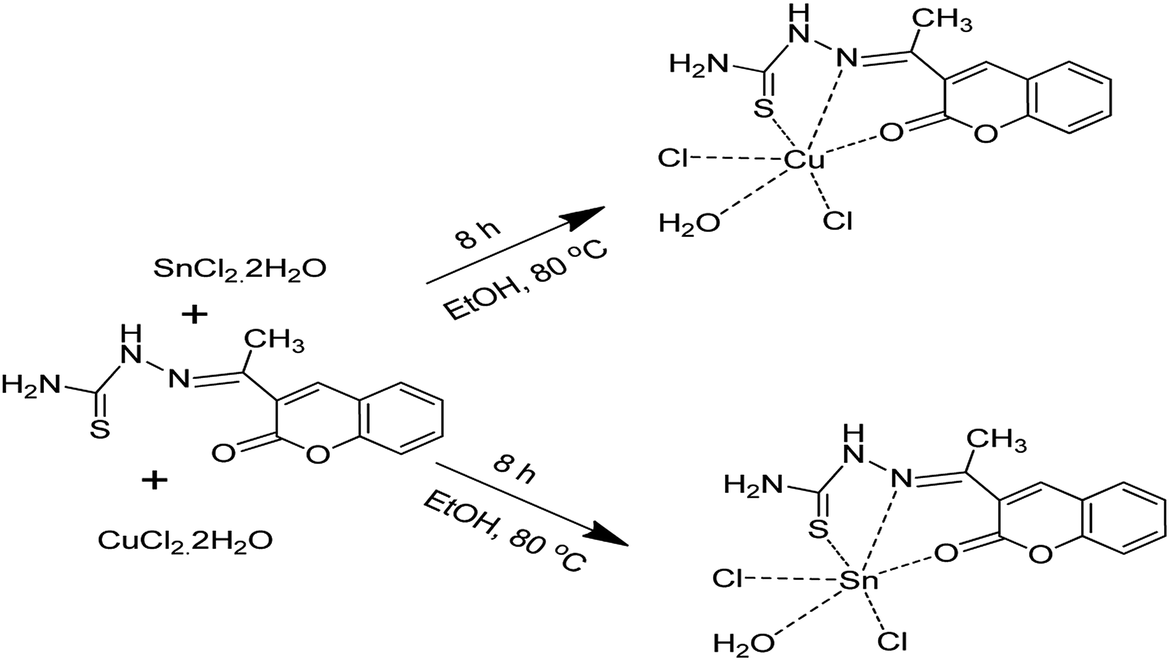 | ||
| Scheme 1 Synthetic pathway for H3L3 and its metal complexes. | ||
Eventual structural elucidation of the (H3L3) motif was confirmed using 1H and 13C NMR. The 1H-NMR spectrum of the ligand in deuterated DMSO showed a 3H singlet at δ 2.25 ppm, while two protons multiplet of aromatic resonated at δ 7.40–7.55 with coupling constant of 8.00 Hz, and another aromatic proton at δ 7.65 ppm resonated as a triplet with a coupling constant of 7.8 Hz close to a fourth Ar–H which resonated as doublet at 7.77 ppm with coupling constant of 7.9 Hz. The singlet at δ 7.99–8.41 ppm was due to the presence of two amide protons one of which was deshielded by the electron withdrawing thioamide bond, while the singlet with chemical shift δ 8.48 ppm was as a result of the hetero ring system of coumarin. The singlet at δ 10.45 ppm is attributed to the proton of the hydrazone. This deshielded downfield resonance of the hyrdrazone proton experienced herein corroborated the properties of Schiff base compounds of carbothioamide origin.24 The 13C NMR spectrum confirmed twelve carbon atoms in the H3L3 ranging from 115.90 to 179.23 ppm as envisaged. The thiocarbamate carbon (C16) and carbonyl carbon (C5) appeared downfield at 179.23 and 158.36 ppm respectively due to their direct attachment to sulphur or oxygen leading to a reduction in their electron density.
The IR spectrum of the ligand shows the following bands characteristic of a carbothioamide: 3385 cm−1 ν (N–H), 1717 cm−1 ν (CO), 1580 cm−1 ν (CN), 1496 cm−1 ν (N–N), 1115 cm−1 ν (C–N) and 1073 cm−1 ν (CS). While the IR spectra of the metal complexes exhibited a distinct bathochromic shift from that of the ligand. The M–O, M–S and M–N bands of all the complexes appeared at the fingerprint region of 756.01–562.17 cm−1.
TGA/DTA analysis of the complexes
The TGA and DTA curves obtained for Cu(II) and Sn(II) complexes in the temperature range 25–600 °C at a heating rate of 10 °C in a nitrogen atmosphere are as shown in Fig. S1 (ESI).† The curve for Cu(II) complex shows that the compound was fairly stable from ambient temperature up to 196 °C. However, the compound decomposed in four steps at 61, 196, 239 and 395 °C as shown in the DTG peaks. The onset of decomposition between 61–92 °C was attributed to the loss of lattice water outside the coordination sphere corresponding to 5% weight loss. At 239–262 °C, a weight loss of about 22% is predicted due to the loss of coordinated aquo- and chloro-ligands. The H3L3, ligand constitutes about 60% of the complex, and accounted for about 51% weight loss in the last decomposition step which occurred between 391–491 °C. Therefore, a residual 22% that occurs above this temperature range can be said to be the contribution of very stable copper sulphide. Similarly, the Sn(II) complex exhibited two major decomposition steps with peaks at 222 and 398 °C. There was a 13% weight loss between 175–250 °C, accounting for the loss of two axial chloro- and aquo-ligands, while the decomposition between 407–483 °C, with 56% weight loss is attributed to the removal of the hydrazinecarbothioamide ligand. The residual 31% accounts for tin(II) sulphide in the complex. The TGA analysis of Cu(II) and Sn(II) complexes has shown the possibility of obtaining a stable material by thermal or solvothermal treatment of the single or mixed precursors.Oleylamine capped CTS nanocrystals obtained via the heat up method
The p-XRD pattern of CTS NPs obtained at 200 and 250 °C by the heat up method in an oleylamine solution of the precursor is shown in Fig. 1. The diffraction peaks show phase pure tetragonal Cu2SnS3 with space group of I![[4 with combining macron]](https://www.rsc.org/images/entities/char_0034_0304.gif) 2m (121) (ICDD# 01-089-4714). The relative highest intensity peak was observed at 2θ = 28.74° corresponding to the (112) plane of tetragonal Cu2SnS3. The major diffraction peaks could be indexed as (112), (004), (114), (213), (204), (310) and (116) reflections of Cu2SnS3.
2m (121) (ICDD# 01-089-4714). The relative highest intensity peak was observed at 2θ = 28.74° corresponding to the (112) plane of tetragonal Cu2SnS3. The major diffraction peaks could be indexed as (112), (004), (114), (213), (204), (310) and (116) reflections of Cu2SnS3.
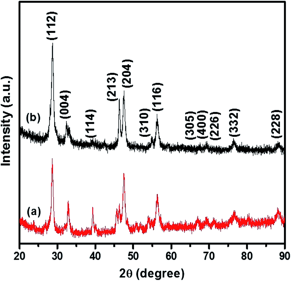 | ||
| Fig. 1 p-XRD pattern of tetragonal CTS NPs obtained at (a) 200 °C and (b) 250 °C when OLA was used both as coordinating solvent and surfactant (heat up). | ||
The relatively lower intensity peak at 2θ = 39.18° was observed at 200 °C (Fig. 1b) an indication of lower degree of crystallinity at lower temperature, making the (114) reflection appear rudimentary. CTS NPs obtained at 200 and 250 °C exhibit preferential growth along the (213) and (204) diffraction planes respectively. The Gaussian fit of the most intense peak (112) was used to calculate the full width at half maximum for the determination of crystallite size. Sizes of ca. 10.9 and 13.4 nm for CTS NPs obtained at 200 and 250 °C respectively, showing that the quantum size effect resulting from peak broadening is predominant at lower synthesis temperature. The results are similar with CTS NPs obtained at different Cu/Sn mole ratios (Fig. S2†), no other p-XRD peaks were observed, indicating the formation of exclusively tetragonal CTS. However, the crystal growth preference for the 2.2:1 Cu/Sn precursor ratio, is towards the (213) plane indicating highest peak intensity for the nanoparticles prepared at 200 °C. No sign of any secondary crystalline phases was found in the p-XRD patterns of nanoparticles obtained at different mole ratios. A summary of different phase transitions obtained under the experimental conditions previously described can be found in Table 2.
| Sample ID/solvent system ratio | T/°C | Phase/formula | Space group | Crystal system | Unit cell | Cal. density g cm−3 | Morphology | Crystallite size (nm) | Particle size (nm) |
|---|---|---|---|---|---|---|---|---|---|
| CTS#1 | 200 | Cu2SnS3 | I2m(121) |
Tetragonal | a = 5.413(1)Å, c = 10.824(1)Å | 1.79 | Nanosheets | 10.9 | 74.03 ± 28.09 |
| CTS#2 | 250 | 13.4 | |||||||
| CTS#4 | 200 | Nanocubes | 8.0 | 9.87 ± 1.71 | |||||
| CTS#6 | 200 | 8.4 | |||||||
| CTS#3 | 250 | Cu4SnS4 | Pnma(62) | Orthorhombic | a = 13.558 Å, b = 7.681 Å, c = 6.412 Å | 4.985 | Nanocubes | 31.4 | 55.70 ± 13.38 |
| CTS#5 | 200 | 9.6 | |||||||
| CTS#7 | 200 | 10.8 | 7.01 ± 0.75 | ||||||
| CTS#8 | 200 | Cu2SnS3 | P1(1) | Mohite, syn | a = 6.64 Å, b = 11.51 Å, c = 19.93 Å, α = 109.75°, β = 90.0° | 4.753 | 8.3 | ||
| CTS#9 | 250 | Anorthic | 15.2 | ||||||
| CTS#10 | 200 | Cu2SnS3 | Cc(9) | Mohite, syn | a = 6.653(1)Å, b = 11.537(2)Å, c = 6.665(1)Å, β = 109.39(3)° | 4.707 | Nanohexagon | 5.0 | 24.85 ± 3.84 |
| Monoclinic |
CTS nanoparticles in OLA and DT mixture
Fig. 2 shows the p-XRD patterns of CTS NPs prepared by the heat up method at different temperatures, 200 and 250 °C. The p-XRD pattern of CTS NPs obtained by injecting 2.0 mL oleylamine into a solution of DT/precursor at 250 °C (Fig. 2c) shows a pure crystalline phase. The high intensity peaks observed at 2θ = 26.57°, 28.04°, 31.01°, 33.77°, 38.02°, 46.70° and 50.94° correspond to the (311), (121), (112), (321), (131), (620) and (223) planes of orthorhombic Cu4SnS4 (ICDD# 029-0584) with space group of Pnma (62). Whereas, the p-XRD patterns obtained for other reaction conditions, whereby 2.0 mL of OLA was injected into a mixture of DT/precursor at 200 °C and subsequently heating up both precursor and surfactant/solvent mixture to 200 °C produced less crystalline CTS NPs with a similar orthorhombic phase (Fig. 2a and b). The crystallite sizes of OLA/DT derived NPs varied with temperature with peak broadening observed at the preferential crystal growth plane (311). The crystallite sizes are ca. 31.4 and 8.0 nm for OLA/DT derived NPs at 250 and 200 °C respectively. The formation of single-phase CTS specifically at 250 °C under the described reaction condition indicates the complete consumption of impurity phases as well as a complete inter-diffusion of the metallic stack. Therefore, the phase transition observed in the p-XRD pattern occasioned by the factor of added dodecanethiol not only provided an impetus of additional surfactant but also an effective sulfurization agent in the formation of the pure phase orthorhombic CTS.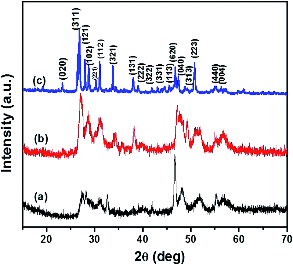 | ||
| Fig. 2 p-XRD patterns of orthorhombic CTS obtained by (a) heat up of precursors in 2.0 mL OLA/6.0 mL DT at 200 °C, (b) injection of 2.0 mL OLA in 6.0 mL DT/precursors at 200 °C and (c) injection of 2.0 mL OLA in 6.0 mL DT/precursors at 250 °C. | ||
Oleylamine capped CTS nanoparticles via hot injection in dodecanethiol (DT)
There was an emergence of different phases as the thermodynamic equilibrium of the synthesis was altered by the mixture of the precursor in OLA, injected into DT at 200 and 250 °C. This approach has been known to alter nucleation and particle growth pattern due to the saturated vapour enhanced dissolution of precursor at elevated temperature. The p-XRD pattern (Fig. S3(a)†) obtained by hot injection of 2.0 mL OLA/precursor at 200 °C into OLA solution displays only the crystalline mohite, syn anorthic Cu2SnS3 phase (ICDD# 027-0198) and space group P1(1) with a preferential orientation (2–11) at 2θ = 28.66° and other intense peaks at 2θ = 30.96°, 32.29°, 46.57°, 47.71° and 56.45° with orientation (040), (0–42), (3–11), (2010) and (3–210) respectively. We also observed a similar pattern in Fig. 5b illustrating a highly crystalline phase of the product obtained by hot injection of OLA/precursor into DT at 250 °C. It is pertinent to note, that preferential crystal growth occurred along the (3–11) plane with more evident prominent peaks due to increased sulphurization. Moreover, (Fig. S3(c)†) illustrates that a different form of Cu2SnS3 was achieved after the hot injection of the OLA/precursor into a solution of DT at 200 °C. In this case, the sulphurization agent produces an evolution from the mohite anorthic CTS to the monoclinic phase, which is detected by the apparition of new peaks at 2θ = 28.48°, 32.29°, 46.93° and 55.69° with orientation (200), (220), (−133) and (−333) respectively (ICDD# 96-152-6188). The crystallite size for both Cu2SnS3 phases are not within close range, with the latter exhibiting a smaller size, ca. 5.0 nm due to the peak broadening effect at lower temperature, while the former was found to give a relatively larger size ca. 15.2 nm by the Scherrer calculation.The structure refinement for CTS#10 was carried out by the Rietveld analysis using FullProf software. The analysis revealed the presence of a CTS pure phase (Fig. 3) which crystallizes in a monoclinic structure with C1c1 space group. As a result of the refinement of the crystal structure by the by the Rietveld method using Fullprof software, the analysis indicated an amount of nearly 94.1(4) (in at%) for the CTS phase, while the remaining 5.9 (in at%) can be assigned to an impurity phase. The obtained values of the refined occupancy states in the CTS phase are within the error bars; α = −0.307(1), β = 0.08(2), λ = 0.04(1) for Cu, Sn, and S respectively. These values are relatively lower than the nominal indicating that the stoichiometric compositions have been achieved.25 Fig. 6 shows the Rietveld refinement for our compound indicating a good agreement between observed and calculated profiles. Detailed result of the refinement is presented in Table S1.†
 | ||
| Fig. 3 Rietveld calculation for monoclinic CTS phase. Observed (Yobs) and calculated (Ycalc) patterns are compared (blue line). The vertical ticks show the positions of the calculated Bragg reflections for the major CTS phase. | ||
Furthermore, an estimate of the average coherent scattering region, CSRs from the broadening of non-overlapping diffraction reflections was also determined for samples CTS#1 and CTS#3 by considering the overlapping reflections from 2θ values between 26–55° for the tetragonal and orthorhombic CTS phases. The p-XRD reflections of the nanopowder were broadened and, therefore, the reflections located close to each other overlapped. The average size D of the coherent scattering region (CSR) estimated from broadening of non-overlapping diffraction reflections (311), (121), (102), (122), (321), (303) and (223) (Fig. 4a) was 65 ± 3 nm (Fig. S4(b)†), while it was 91 ± 6 nm (Fig. S4(a)†) for (112), (004), (114) and (204) orientations in the tetragonal phase CTS (Fig. 2b).
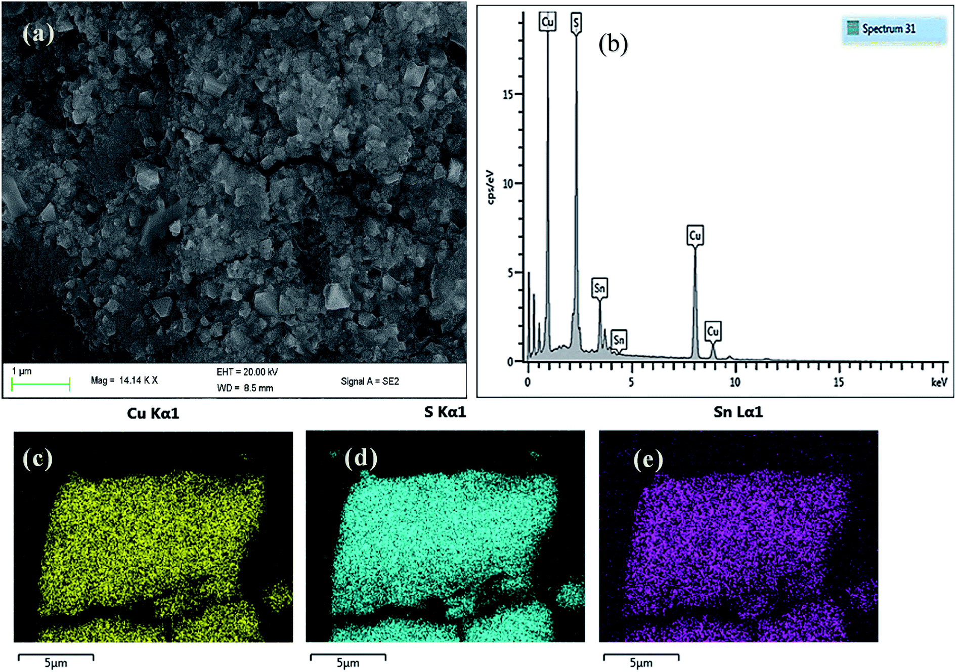 | ||
| Fig. 4 (a) SEM image (b) EDX spectrum and elemental mapping of (c) Cu, (d) S and (e) Sn of tetragonal CTS NPs in OLA at 200 °C. | ||
It is pertinent to state that when the coordinates of Cu, S and Sn atoms and unit cell parameters for Cu2SnS3 nanopowder (Table 2) are close to those for coarse crystalline Cu2SnS3, the occupancy of crystallographic positions by Cu(1) and Cu(2) atoms are nominally approximated to unity.26,27 Therefore, Cu2SnS3 nanoparticles of sizes less than 50 nm are non-stoichiometric, have a composition containing vacant sites in the metal sub-lattice.
Elemental analysis and morphological properties of CTS nanoparticles
The SEM image of CTS NPs in Fig. 4a, obtained by heating up the precursor in OLA, shows the growth of cube-like crystal structures at 200 °C. The energy-dispersive X-ray (EDX) spectroscopy shown in Fig. 4b, displays a slightly copper deficient CTS. The compositional ratio of Cu/Sn was found to be about 1.9 (Table S2†) corresponding to the condition of the appearance of Cu vacancies that provides p-type conductivity.28 This deficiency in atomic composition has been corroborated by Rietveld refinements analysis. The p-type conductivity due to Cu vacancies has also been observed earlier in CZTS.29EDX elemental mapping was carried out, the images (Fig. 4c–e) show the homogenous distribution of Cu, Sn and S elements along the K-line in the cube-like CTS NPs. The atomic composition (Table S2†) indicates that at microscopic level, the stoichiometry of the sample is close to the original formula Cu2SnS3 (33.33% of Cu, 16.67% of Sn and 50% of S). Copper and tin are a little overestimated while sulphur is underestimated.
The morphology and size determination by TEM analysis is shown in Fig. 5. The CTS phases obtained by heat up at 200 and 250 °C showed a different morphology, nanosheet-like structures of Cu2SnS3 (Fig. 5a) with broad size distribution were obtained at 200 °C with OLA acting as a solvent and surfactant medium. The length of the nanosheet (n = 20) averaged 74.03 ± 28.09 nm. Nanocubes of CTS with an average diameter of 55.70 ± 13.38 nm (n = 20) and comparatively better size distribution were formed in OLA/DT solvent at 250 °C (Fig. 5b).
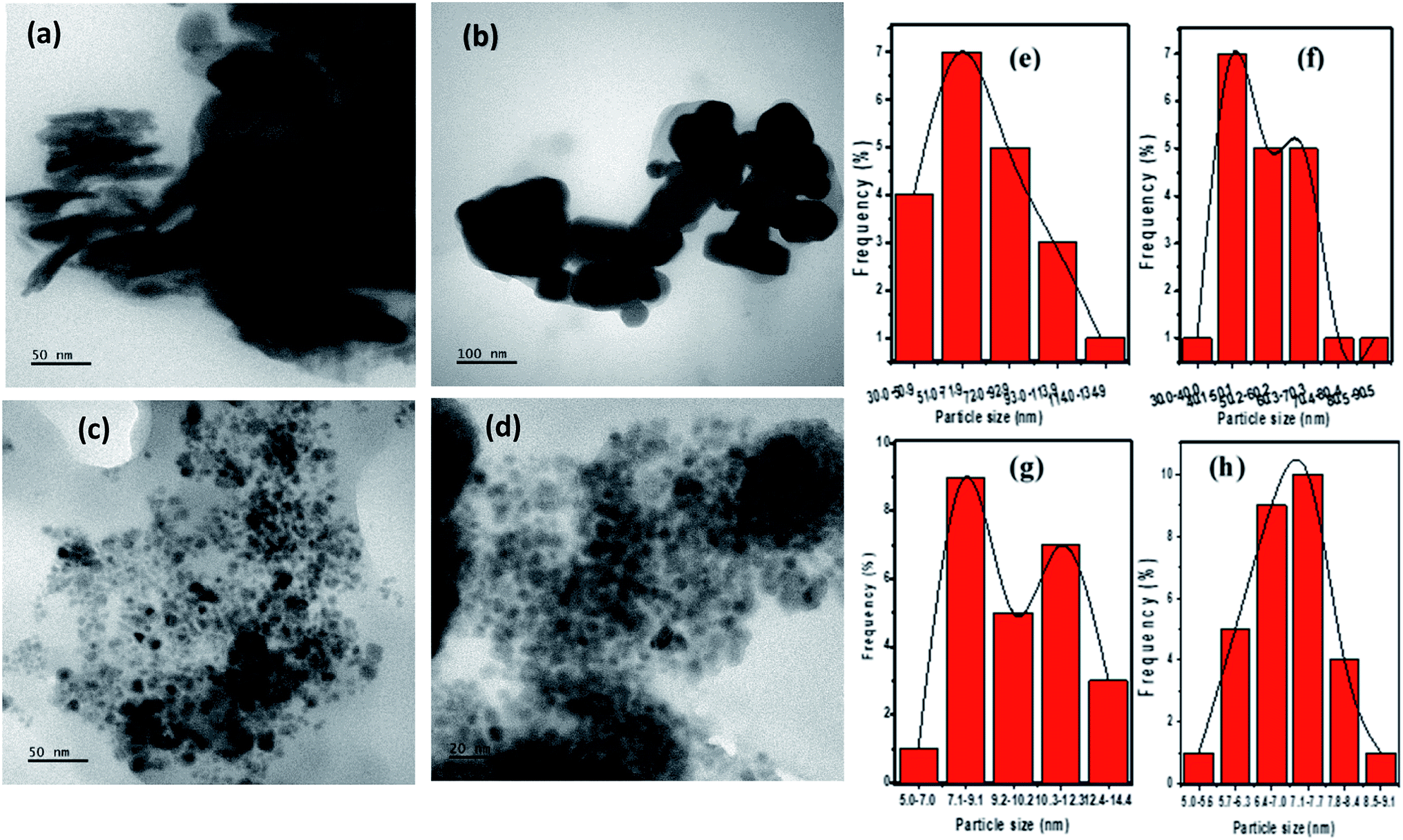 | ||
| Fig. 5 TEM micrographs of (a) CTS nanosheets obtained by heat up in OLA at 200 °C (b) CTS nanocubes obtained by heat up in OLA/DT at 250 °C (c) CTS nanocubes formed by 1.7:1 Cu/Sn ratio at 200 °C (d) CTS nanocubes in OLA/DT at 200 °C and (e–h) their corresponding particle size histogram. | ||
The formation of different phases and morphology of CTS NPs under these temperature and solvent conditions can be explained in terms of the thermodynamics of the precursor in the solvent/surfactant mixture reaction. DT has been a well tried capping ligand and has the ability to enhance cation exchange in copper chalcogenides by extracting copper from the lattice. The thiol oxidation and subsequent Cu reduction was enhanced by the basic environment provided from the amine. Attempts to utilize non-amine base, trioctylphosphine (TOP) did not result in dissolution. Thus, the proposed reaction mechanism (Scheme 2) shows the formation of amine-thiol adduct with solvothermal reduction of Cu2+ to Cu+ ion in the presence of a nucleophilic organic solvent/surfactant, oleylamine. In this medium the Cu–S complex is formed and is stable at high temperature. As thermal equilibrium is achieved Cu+ is released. At the same time, under this reaction condition, Sn2+ is being oxidized to Sn4+ by the action of Cu2+. The compounds with Cu exclusively in the 1+ oxidation state (Cu4SnS4, Cu2SnS3) are expected to be better solar absorbers than those with Cu in a mixed 1+/2+ oxidation state, as the multi-valency of Cu can lead to high carrier concentrations (∼1022 cm−3) or hole self-trapping.30–36
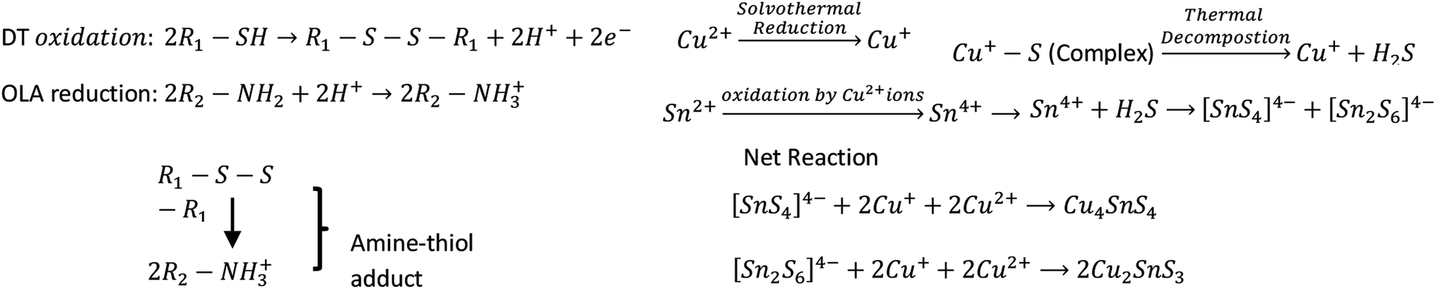 | ||
| Scheme 2 Proposed reaction mechanism for Cu4SnS4 and Cu2SnS3 NPs. | ||
The effect of variation of Cu/Sn ratio on the morphology of CTS NPs in OLA at 200 °C can be seen in Fig. 5c, smaller monodispersed nanocubes were produced which averaged 9.87 ± 1.71 nm (n = 25). At the same temperature, quantum sized well dispersed nanocubes (Fig. 5d) were obtained in a DT/OLA mixture which measured 7.01 ± 0.75 nm (n = 30).
Similarly, different CTS NPs were obtained under enumerated reaction conditions by the hot injection of OLA into OLA or DT at 200 °C and 250 °C respectively. Nanodiscs (Fig. S5(a)†) and nanosphere-like structures (Fig. S5(b)†) of CTS were found at 200 °C and 250 °C respectively. Whereas, faceted CTS (Fig. S5(c and d)†), which an average size of 24.85 ± 3.84 nm (n = 40), were obtained at 200 °C by injection of the OLA/precursor mixture into DT. The particle size histogram (Fig. S5(e)†) shows a narrow size distribution, attesting to the monodispersity of the NPs.
Optical properties
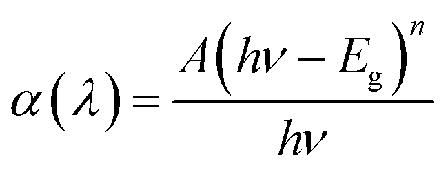
The optical band gap energy (Eg) of the CTS films was calculated from the equation given below,where A is a constant and n defines the nature of the transition, h is Planck's constant and ν is frequency of light. For direct allowed optical transitions, n is 1/2.37,38
The band gap energy calculation was performed by extrapolating the linear region of plot (αhν)2 versus hν to the horizontal axis and considering the intersecting point. Fig. 6c and d shows the estimated band gap energy of the CTS NPs in OLA obtained at different temperature. The UV-Vis spectra show broad range absorbance between 400–600 nm (Fig. 6a). For both spectra, the absorbance increase is observed in the near edge region which suggests the bandgap value to be found in the near infrared region. Since the Cu2SnS3 phase represents a direct band-gap semiconductor, Tauc plots can be used to find Eg value by plotting (αhν)2 as a function of the photon energy (eV) and extrapolating the linear portion of the spectrum in the band edge region. The values of approximately 1.13 eV for CTS#1 and 1.18 eV for CTS#2 were determined as shown in the insets (c) and (d) of Fig. 6, respectively. These values are in a good agreement with those reported by other groups for CTS but are slightly higher than expected for the proposed tetragonal phase.39 Observed values of Eg seem to be suitable for photovoltaic applications.
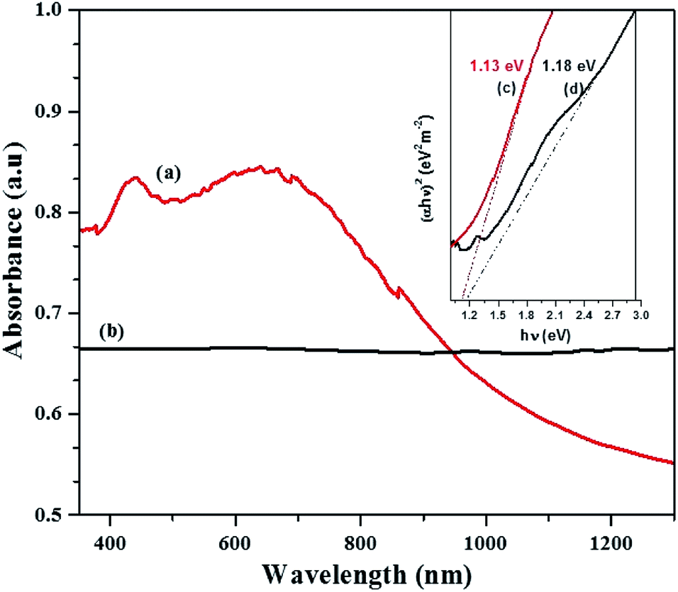 | ||
| Fig. 6 Optical spectra of CTS tetragonal NPs obtained by heat up method in OLA (a) at 200 °C (b) 250 °C and their respective Tauc plot, inset (c and d) with extrapolated band gap energy. | ||
For the orthorhombic Cu4SnS4 phase obtained by heat up in OLA/DT at 200 °C and 250 °C, typical featureless absorbance spectra are shown in Fig. 7a–c which exhibit a broad band between 650–850 nm. The inset plots in Fig. 7 show that the highest optical bandgap of 1.45 eV (Fig. 7d) was obtained at lower temperature, 200 °C, while the lowest 1.05 eV (Fig. 7e) resulted at 250 °C. Thus, the absorption onset is red-shifted, compared with the orthorhombic Cu3SnS4 (band gap 1.55 eV). This might be due to the minor stoichiometric variation or presence of other phases, most likely, other modifications of CTS, such as the tetragonal Cu3SnS4 phase with a bandgap of 1.2 eV.40,41 Similarly, for the mohite anorthic and monoclinic phases obtained by the hot injection method, characteristic broad band absorbance measured between 500–800 nm (Fig. 8a–c) can be observed. The reported band gap values (inset Fig. 8d and e) for anorthic at 200 °C and 250 °C are 1.35 and 1.16 eV, respectively, while the monoclinic phase at 200 °C measured 1.46 eV (inset Fig. 8f). The different band gaps of these structures are due to different geometrical arrangements of the cations and anions in the atomic structures.
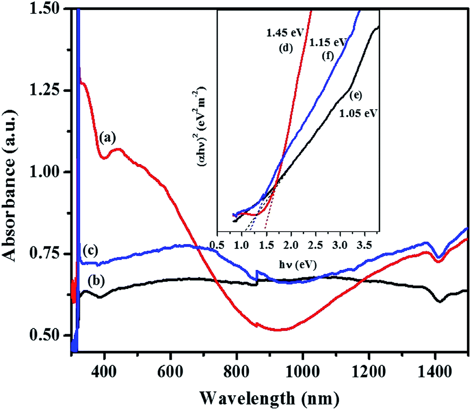 | ||
| Fig. 7 Optical spectra of orthorhombic CTS obtained by heat up method after injecting OLA into DT/precursor at (a) 200 °C and (b) 250 °C; (c) heating up OLA/DT/precursor to 200 °C and their corresponding Tauc plots, inset (d–f) with extrapolated band gap energy. | ||
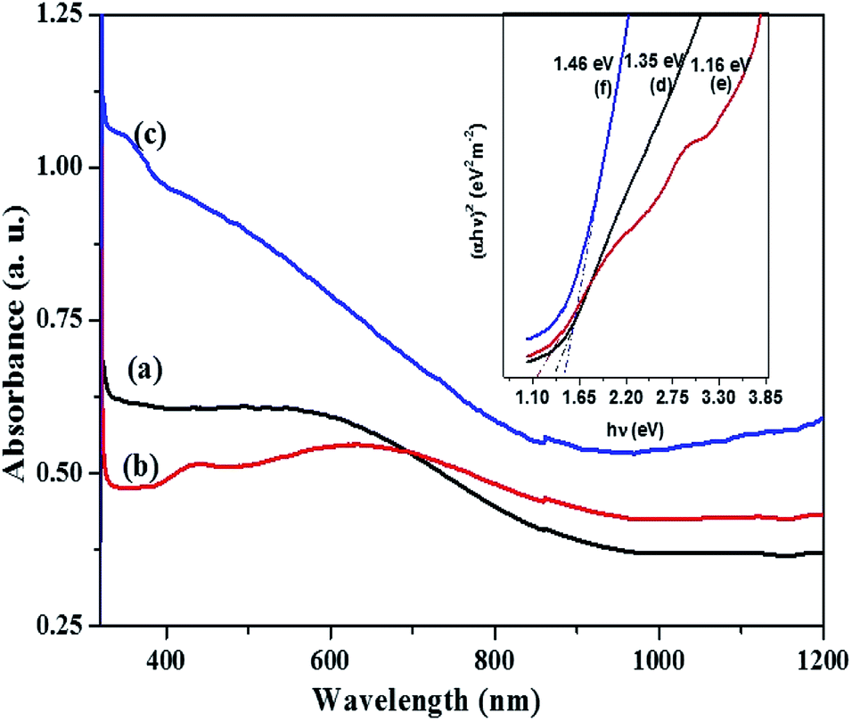 | ||
| Fig. 8 Optical spectra of CTS NPs obtained by hot injection of OLA/precursor into (a) OLA at 200 °C (b) DT at 250 °C (c) DT at 200 °C and their corresponding Tauc plots, inset (d–f) with extrapolated band gap energy. | ||
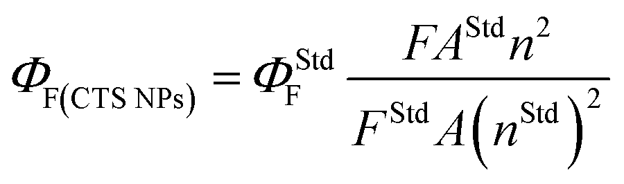
Fig. 9 and S6† show the emission spectra of the CTS NPs prepared by the heat up and hot injection methods. By irradiating very dilute solutions of the CTS# samples with wavelengths ranging from 330–370 nm at triple excited states, uniform emission peaks were recorded in the 432–433 nm range (Fig. 9a and b). The emission maximum was observed at 2.86 eV under excitation with 3.76 eV radiation (Fig. 9c). This corresponds to the band to band transition in CTS NPs as also determined from the absorbance spectra in Fig. 6–8. Since these materials showed promising light absorbing property, the fluorescence quantum yields (ΦF) of the CTS NPs were also determined by the comparative method42 using the following equation:
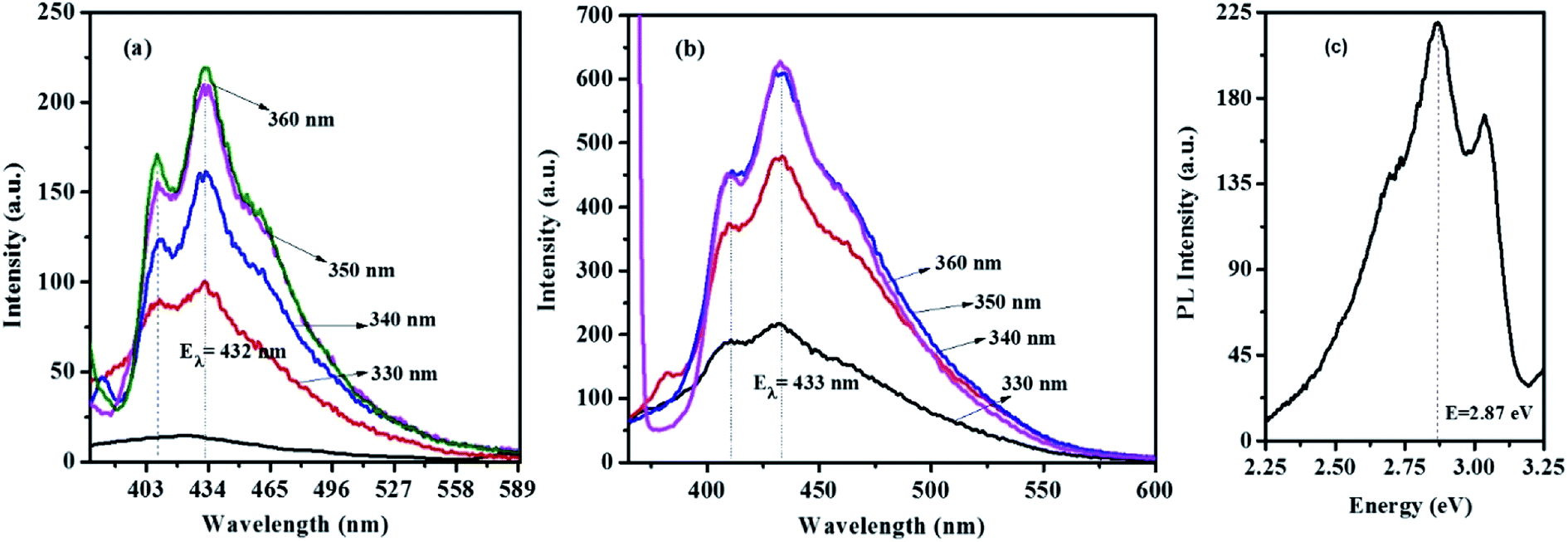 | ||
| Fig. 9 Optical emission spectra of CTS NPs obtained by heat up method in (a) OLA at 200 °C (b) OLA/DT at 200 °C (c) energy equivalence of the CTS NPs emission. | ||
Quinine sulphate in 0.1 M H2SO4 (ΦF = 0.52)43 was employed as reference standard. The quantum yields found for CTS NPs reported in this work are 0.009 (0.9%) and 0.023 (2.3%) for the NPs obtained by hot injection at 200 and 250 °C respectively. The luminescence quantum yield (Φ) is the ratio of the number of photons emitted to the number of photons absorbed. Therefore, the maximum value of Φ is 1. In practice, the quantum yield is less than unity for virtually all luminescent materials. The values here are in agreement with the expected nonzero quantum yield for emission between 397 and 430 nm (ref. 25 and 42) which is believed to be due to a contribution from internal vibrational and rotational energy as well as to a small contribution from collisions.
Conclusions
The various crystal phases, size, shapes and the yield of CTS nanoparticles, depend upon the type of chemical method adopted for synthesis. Solvothermal method can be preferred for CTS nanoparticle synthesis if the nanoparticles are used for energy storage devices and photocatalytic application as these methods produce good quality and crystalline nanocrystals. Hot injection and heat up methods were adopted in this work to ensure precise control over size, phase and desired composition. Rietveld refinement for the monoclinic phase indicated a good agreement between observed and the calculated profiles which showed that stoichiometric compositions have been achieved. The calculated band-gap energies of 1.05–1.45 eV are in the optimum range for photovoltaic applications. The compounds with Cu exclusively in the 1+-oxidation state (Cu4SnS4, Cu2SnS3) are expected to be better solar absorbers than those with Cu in a mixed 1+/2+ oxidation state, as the multivalency of Cu can lead to high carrier concentrations (∼1022 cm−3) or hole self-trapping.Conflicts of interest
Authors declare no conflict of interest.Acknowledgements
The authors are grateful to the National Research Foundation (NRF) South Africa through the South African Research Chair Initiative (SARChI) for financial support.Notes and references
- D. B. Mitzi, O. Gunawan, T. K. Todorov, K. Wang and S. Guha, Sol. Energy Mater. Sol. Cells, 2011, 95, 1421–1436 CrossRef CAS.
- U. Ghorpade, M. Suryawanshi, S. W. Shin, K. Gurav, P. Patil, S. Pawar, C. W. Hong, J. H. Kim and S. Kolekar, Chem. Commun., 2014, 50, 11258–11273 RSC.
- P. Jackson, D. Hariskos, E. Lotter, S. Paetel, R. Wuerz, R. Menner, W. Wischmann and M. Powalla, Prog. Photovoltaics, 2011, 19, 894–897 CAS.
- M. Ristov, G. Sinadinovski, M. Mitreski and M. Ristova, Sol. Energy Mater. Sol. Cells, 2001, 69, 17–24 CrossRef CAS.
- T. A. Kuku and O. A. Fakolujo, Sol. Energy Mater., 1987, 16, 199–204 CrossRef CAS.
- Y. T. Zhai, S. Chen, J. H. Yang, H. J. Xiang, X. G. Gong, A. Walsh, J. Kang and S. H. Wei, Phys. Rev. B: Condens. Matter Mater. Phys., 2011, 84, 075213 CrossRef.
- S. Fiechter, M. Martinez, G. Schmidt, W. Henrion and Y. Tomm, J. Phys. Chem. Solids, 2003, 64, 1859–1862 CrossRef CAS.
- G. Phaneendra Reddy and K. T. Ramakrishna Reddy, Mater. Today: Proc., 2017, 4, 12518–12524 Search PubMed.
- S. Dias, B. Murali and S. B. Krupanidhi, Mater. Chem. Phys., 2015, 167, 309–314 CrossRef CAS.
- P. A. Fernandes, P. M. P. Salomé and A. F. d. Cunha, J. Phys. D: Appl. Phys., 2010, 43, 215403 CrossRef.
- D. Avellaneda, M. T. S. Nair and P. K. Nair, J. Electrochem. Soc., 2010, 157, D346–D352 CrossRef CAS.
- S. A. Vanalakar, G. L. Agawane, A. S. Kamble, C. W. Hong, P. S. Patil and J. H. Kim, Sol. Energy Mater. Sol. Cells, 2015, 138, 1–8 CrossRef CAS.
- H. D. Shelke, A. Lokhande, V. S. Raut, A. M. Patil, J. H. Kim and C. D. Lokhande, J. Mater. Sci.: Mater. Electron., 2017, 28, 7912–7921 CrossRef CAS.
- M. D. Khan, M. Aamir, M. Sohail, S. Bhoyate, M. Hyatt, R. K. Gupta, M. Sher and N. Revaprasadu, Dalton Trans., 2019, 48, 3714–3722 RSC.
- T. Alqahtani, M. D. Khan, D. J. Kelly, S. J. Haigh, D. J. Lewis and P. O'Brien, J. Mater. Chem. C, 2018, 6, 12652–12659 RSC.
- C. Gervas, M. D. Khan, C. Zhang, C. Zhao, R. K. Gupta, E. Carleschi, B. P. Doyle and N. Revaprasadu, RSC Adv., 2018, 8, 24049–24058 RSC.
- M. D. Khan, G. Murtaza, N. Revaprasadu and P. O'Brien, Dalton Trans., 2018, 47, 8870–8873 RSC.
- M. D. Khan, M. Aamir, G. Murtaza, M. A. Malik and N. Revaprasadu, Dalton Trans., 2018, 47, 10025–10034 RSC.
- S. A. Saah, M. D. Khan, P. D. McNaughter, J. A. Awudza, N. Revaprasadu and P. O'Brien, New J. Chem., 2018, 42, 16602–16607 RSC.
- J. Guo, Y. Cao, R. Shi, G. I. N. Waterhouse, L. Z. Wu, C. H. Tung and T. Zhang, Angew. Chem., Int. Ed., 2019, 58, 8443–8447 CrossRef CAS.
- A. Tyagi, G. K. Kole, A. Y. Shah, A. Wadawale, A. P. Srivastava, M. Kumar, G. Kedarnath and V. K. Jain, J. Organomet. Chem., 2019, 887, 24–31 CrossRef CAS.
- L.-S. Wang, T.-L. Sheng, X. Wang, D.-B. Chen, S.-M. Hu, R.-B. Fu, S.-C. Xiang and X.-T. Wu, Inorg. Chem., 2008, 47, 4054–4059 CrossRef CAS.
- B. Qu, M. Zhang, D. Lei, Y. Zeng, Y. Chen, L. Chen, Q. Li, Y. Wang and T. Wang, Nanoscale, 2011, 3, 3646–3651 RSC.
- O. O. Ajani and O. C. Nwinyi, J. Heterocycl. Chem., 2010, 47, 179–187 CAS.
- F. Belkhiria, F. I. H. Rhouma, S. Hcini, M. Daoudi, H. Gammoudi, M. Amlouk and R. Chtourou, J. Lumin., 2017, 181, 1–7 CrossRef CAS.
- Y. Liu, M. Liu, D. Yin, W. Wei, P. N. Prasad and M. T. Swihart, Chem. Mater., 2017, 29, 3555–3562 CrossRef CAS.
- S. I. Sadovnikov and A. I. Gusev, J. Mater. Chem. A, 2017, 5, 17676–17704 RSC.
- A. Kanai, K. Toyonaga, K. Chino, H. Katagiri and H. Araki, Jpn. J. Appl. Phys., 2015, 54, 08KC06 CrossRef.
- E. Peksu, M. Terlemezoglu, M. Parlak and H. Karaagac, Renewable Energy, 2019, 143, 1133–1142 CrossRef CAS.
- F. Chen, J. Zai, M. Xu and X. Qian, J. Mater. Chem. A, 2013, 1, 4316–4323 RSC.
- Y. Xiong, Y. Xie, G. Du and H. Su, Inorg. Chem., 2002, 41, 2953–2959 CrossRef CAS.
- P. Zawadzki, L. L. Baranowski, H. Peng, E. S. Toberer, D. S. Ginley, W. Tumas, A. Zakutayev and S. Lany, Appl. Phys. Lett., 2013, 103, 253902 CrossRef.
- B. C. Walker and R. Agrawal, Chem. Commun., 2014, 50, 8331–8334 RSC.
- W. Wei, W. Chen, L. Ding, S. Cui and L. Mi, Nano Res., 2017, 10, 3726–3742 CrossRef CAS.
- W. Wei, J. Wu, S. Cui, Y. Zhao, W. Chen and L. Mi, Nanoscale, 2019, 11, 6243–6253 RSC.
- W. Wei, W. Ye, J. Wang, C. Huang, J.-B. Xiong, H. Qiao, S. Cui, W. Chen, L. Mi and P. Yan, ACS Appl. Mater. Interfaces, 2019, 11, 32269–32281 CrossRef CAS.
- P. R. Ghediya, T. K. Chaudhuri, V. Raj, D. Chugh, K. Vora, L. Li, H. H. Tan and C. Jagadish, Mater. Sci. Semicond. Process., 2018, 88, 120–126 CrossRef CAS.
- G. Phaneendra Reddy and K. T. Ramakrishna Reddy, Mater. Today: Proc., 2017, 4, 12401–12406 Search PubMed.
- H. Dahman, S. Rabaoui, A. Alyamani and L. El Mir, Vacuum, 2014, 101, 208–211 CrossRef CAS.
- M. Kruszynska, J. Parisi and J. Kolny-Olesiak, Naturforscher, 2014, 69, 446 CAS.
- M. Bouaziz, M. Amlouk and S. Belgacem, Thin Solid Films, 2009, 517, 2527–2530 CrossRef CAS.
- S. Fery-Forgues and D. Lavabre, J. Chem. Educ., 1999, 76, 1260 CrossRef CAS.
- M. Brouwer Albert, Pure Appl. Chem., 2011, 83, 2213 Search PubMed.
Footnote |
| † Electronic supplementary information (ESI) available: TGA, p-XRD and EDX, electrochemical plots and tables. See DOI: 10.1039/c9ra07376k |
| This journal is © The Royal Society of Chemistry 2019 |