
 Open Access Article
 This Open Access Article is licensed under a Creative Commons Attribution-Non Commercial 3.0 Unported Licence
Spin-layer locked gapless states in gated bilayer graphene†
W. Jaskólski a and
A. Ayuela*bc
a and
A. Ayuela*bc
aFaculty of Physics, Astronomy and Informatics, Institute of Physics, Nicolaus Copernicus University, Grudziadzka 5, 87-100 Toruń, Poland. E-mail: wj@fizyka.umk.pl
bDonostia International Physics Center (DIPC), Manuel de Lardizabal 4, E-20018 San Sebastián, Spain
cCentro de Física de Materiales-MPC CSIC-UPV/EHU, Manuel de Lardizabal 5, E-20018 San Sebastián, Spain. E-mail: swxayfea@sw.ehu.es
First published on 19th December 2019
Abstract
Gated bilayer graphene exhibits spin-degenerate gapless states with a topological character localized at stacking domain walls. These states allow for one-dimensional currents along the domain walls. We herein demonstrate that these topologically protected currents are spin-polarized and locked in a single layer when bilayer graphene contains stacking domain walls decorated with magnetic defects. The magnetic defects, which we model as π-vacancies, perturb the topological states but also lift their spin degeneracy. One gapless state survives the perturbation of these defects, and its spin polarization is largely localized in one layer. The spin-polarized current in the topological state flows in a single layer, and this finding suggests the possibility of effectively exploiting these states in spintronic applications.
Introduction
Bilayer graphene (BLG) has attracted a great deal of attention because it can exist with a variety of stacking arrangements with intriguing electronic properties.1,2 Of particular note is the revival of interest in twisted layers of graphene due to their superconductivity.3 In the search for graphene-based systems for nanoelectronic applications,4–10 Bernal-stacked BLG has considerable promise as it possesses a tunable energy gap under an applied gate voltage.11–14 Furthermore, gated BLG containing stacking domain walls (SDWs) shows conducting gapless states, which are topologically protected and well defined in terms of the valley index.15–18 These states continue to attract attention for their potential applications in novel devices and as testing grounds for topological phases in 2D materials.19,20The existence of topological states has been reported in experiments on gapped BLG.21,22 Topological states appear as a pair of states connecting the valence and conduction band continua in the energy gap of gated BLG.15,17,18,20 They are induced by SDWs, i.e., when the order of the sublattice changes from AB to BA. Experimentally, a SDW can be realized by stretching, corrugating, folding, or introducing defects in one of the layers.18,21,23,24 In a bilayer, topological states allow for transport along the domain wall.18 These states are robust and topologically protected because the valley Chern number changes across the SDW.16,20 Although these states were first described in topological terms, atomistic modelling is required to study their physico-chemical properties in experimental realizations.25 Atomistic calculations extend beyond topological considerations and predict the survival of topological states in cases with atomic-scale defects present in SDWs.24
The conducting states that arise at the one-dimensional boundary between two regions of gated BLG with different stacking orders are topologically valley protected.16 The gapless states are thus locked in their momentum and characterized by pseudospin due to the sublattice symmetry. Additionally, the states are spin degenerate, and it may be necessary to remove the spin degeneracy for future applications, e.g., spintronic devices. According to Lieb's theorem for π-vacancies in 2D systems, the spin degeneracy can be removed by a magnetic signal driven by a local imbalance between the A and B sublattices.26 Graphene π-vacancies can be created by a large number of experimental methods using Co substituents, radicals, H-doping, and even fluorination.27,28 The π-vacancies in pristine graphene lead to the appearance of localized states and magnetic moments;29–31 these states appear at zero energy and are spin split into a couple of spin-polarized states due to the locally uncompensated sublattices.32–34 Other works investigate the vacancies in graphene using STM techniques35 and even report a magnetic signal.36 Then, we have to study how the spin degeneracy of gapless states is removed by magnetic defects near SDWs in BLG.
In this work, we consider the vacancy defects close to the SDW in one of the layers of BLG and investigate their interplay with topological gapless states. For vacancy defects near the SDW, the defect states interact with the topologically protected states in the gap, and the landscape of the states spanning the gap changes. Despite the strong perturbation caused by vacancies, we find a topologically protected gapless state that is spin split. The ability to obtain two gapless channels with different spin orientations, i.e., a characteristic of topological insulators, is valuable. Although the spin is not locked to the momentum, we find that one of the two spin channels is strongly locked to the layer with vacancies. This result is our most significant observation and implies that vacancy defects can drive the current flow in the domain wall predominantly to one layer and one spin orientation, which indicates a potential route for the design of a new type of electronic device that could exploit features combining spintronics and layertronics.25
Model and methods
We investigate BLG with vacancies close to a SDW, as schematically shown in Fig. 1. We consider the minimal domain wall because the appearance of topological states is independent of whether the SDW is sharp25 or smooth,15 formed by grain boundaries24 or corrugations in a layer.18,37 Note that when the domain wall region is smooth, the interchange region between AB and BA stackings increases. Because the transition region acts as a gapless medium, the topological states propagate therein as extended states preserving their low localization. Thus the major findings discussed here on the interaction between magnetic π-vacancies and topological states in the gap would hold.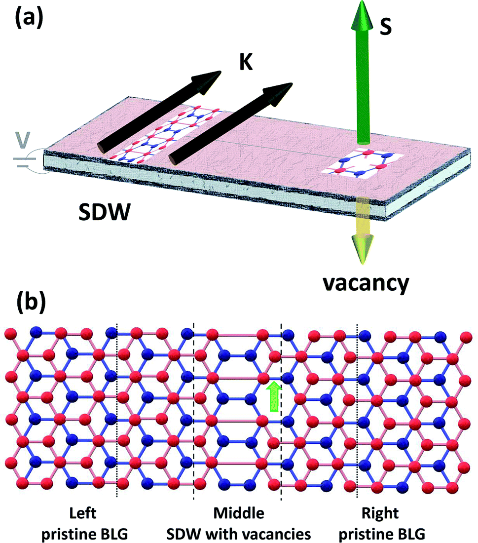 | ||
| Fig. 1 (a) Schematic representation of the investigated BLG, including a SDW and vacancies. The topological gapless states locked to the K valley and momentum are displayed as a couple of arrows along the SDW. The green-yellow arrows indicate the vacancy and the related up–down components in the magnetic moment. (b) An example of the system unit cell, which repeats periodically in the vertical (zigzag) direction. The SDW with vacancies is situated in the upper (red) layer of the central part embedded between the left and right leads of pristine BLG. Vertical dashed lines mark the interface between the central part and the leads; vertical dotted lines mark the building blocks in the leads. | ||
The system studied is divided into three regions:38 pristine BLG on the left- and right-hand sides of the SDW is treated as the semi-infinite leads (L, R) and the central region (C) includes the SDW with nearby vacancies located in the upper layer. Both, the leads and the central part extend to infinity along the zigzag direction because there is translation symmetry along the SDW. A fragment of the unit cell (which is infinite in the direction perpendicular to SDW) is shown in Fig. 1(b). There is only one vacancy per unit cell. The leads are built as infinite sequence of slabs, which extend to the left/right from the interface with the central region. The size of the unit cell in the SDW direction depends on the separation between consecutive vacancies. In the case presented in Fig. 1(b) the vacancies appear every fourth graphene unit cell along the SDW, i.e., they are separated by ≈9. In this case the central part of the system unit cell and the slabs of the leads contain 32 carbon atoms each. When the vacancies are more defused or appear farther away from the SDW, the corresponding unit cells are larger and contain more atoms.
To calculate the local density of states (LDOS), we employ the Green function matching technique.38–41 First, the Hamiltonians HC, HL and HR for the central region and the slabs of the left and right leads are generated. They are self-consistently calculated in the mean-field Hubbard model within the π-electron approximation, removing the zigzag edge states. We use the values of intralayer γ0 and interlayer γ1 hoppings equal −2.7 eV and 0.1γ0, respectively,11,12 and the value of the on-site Coulomb interaction term U = 2.8 eV.42,43 Based on the HL/R/C Hamiltonians and the transfer matrix technique38,44 the Green function GC for the central region is found and the LDOS calculated according the formula  where Tr means the trace of the corresponding GC matrix. The resulting LDOS is k-dependent due to the periodicity along the zigzag direction. In the self-consistent calculations of the Hubbard Hamiltonians, 2000 k points and the convergence precision up to 10−6 eV at the Fermi level are used. The large number of the k and the energy E values (also 2000) is necessary for precise calculation and visualization of the LDOS.
Results
We now study the electronic structure of gated BLG with a SDW decorated with vacancies, as shown in Fig. 1. A voltage V = 0.18 eV is applied to the bottom layer. The corresponding LDOS for the middle region including the SDW with vacancies, as per Fig. 1, is shown in Fig. 2. The green and yellow arrows identify the spin-up and spin-down bands, respectively. The spin-up and spin-down states in the valence and conduction band continua are superimposed because the induced spin splitting is considered to be almost negligible.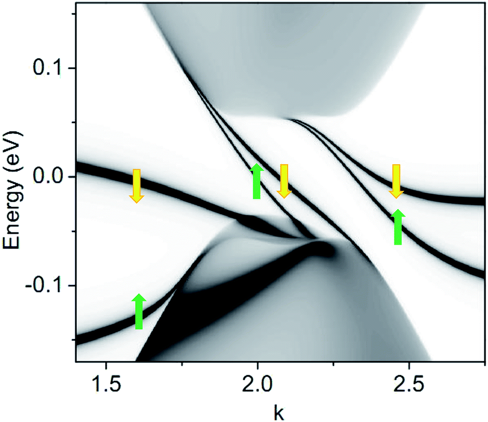 | ||
| Fig. 2 Energy structure near the Fermi level (zero-energy) for gated BLG with SDW and vacancies. The k values are given in units of π/a, where a is the period length in the zigzag direction and set as a = 1. A gapless state is present in the band gap connecting the valence and conduction bands at the cone, and it is spin split due to the interaction with the vacancy band. | ||
Away from the cone on the left- and right-hand sides, we find two spin-polarized states. These stem from the spin-split vacancy states, which strongly interact with the corresponding topological states close to the cone due to the SDW. A detailed analysis of these vacancy states confirms their strong localization in the upper layer; the spin-polarized LDOS in the upper layer is a few orders of magnitude higher than that in the lower layer.
At the cone, two spin-polarized states span the entire energy gap. They appear as a result of the interaction and mixing of the two spin-degenerate topological states at the SDW with the spin-split vacancy band. The most striking result is the persistence of a topological spin-split state in the gap, despite the strong interaction of the electronic structure of BLG with the SDW caused by the vacancy defects.
Most of the spin-down vacancy band in the left side of the cone lies above the Femi level and is unoccupied. Therefore, the total magnetic moment in the middle region is about 0.5 μB. The moment obtained by uncompensated sublattices due to the vacancy is reduced from the a priori value of 1 μB because the leads are passing charge to the vacancy and the SDW region.
We also perform calculations for other systems with different distances between consecutive vacancies or between vacancies and the SDW. No significant differences are observed in the trends of the results presented in Fig. 2. The splitting slightly decreases when the distance between vacancies increases. Similarly, when the vacancies move away from the SDW region, their role in the extended gapless states weakens, and the spin-splitting slightly decreases. The decrease in the spin-splitting of the topological state for the sparse distribution of vacancies can be easily explained; the gapless states are spatially located along the SDW and decay away from the domain wall.18
The vacancies are periodically distributed along the SDW. Each vacancy introduces a local zero-energy state with a local magnetic moment, which interacts with the topological states, so that they have spin splitting. As mentioned above, the splitting slightly depends on the site of the vacancy with respect to the SDW. Anyhow, we may reasonably assume that spin-splitting of the gapless states occurs even when magnetic defects are not perfectly periodically distributed along SDWs.
To understand the interplay between the topologically protected states and vacancy states, we remove the observed spin polarization. We performed LDOS calculations with the on-site Coulomb interaction set to zero, i.e., hindering spin-splitting of the involved states. The results are shown in the ESI.† After strong interaction and mixing of the pair of topological gapless states with the vacancy band one gapless state survives before spin polarization is included. This finding is further clarified by modelling the interaction of the spin-degenerate gapless states with the localized vacancy state. We use a three-band Hamiltonian:
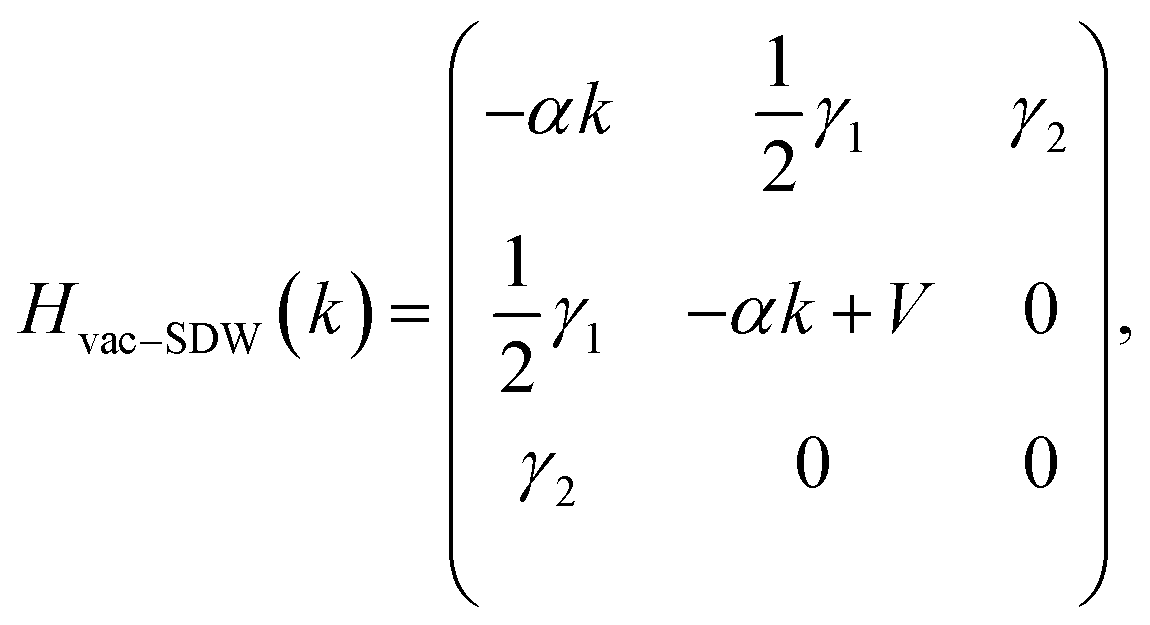 | (1) |
We next investigate the spin-polarization gain of the topological states after including the vacancy states and how this gain depends on the gate voltage. We consider the layer-resolved LDOS for the spin-up and spin-down gapless states at the Fermi energy. This LDOS is calculated by accounting for the contribution from the atoms in the middle region and integrating over k-values in a range of ±0.1 around the point where the topological state crosses the Fermi level. Fig. 3(a) and (b) show the LDOS in the lower and upper layers for two values of gate voltage V = 0.18 eV and V = 0.36 eV, respectively. Horizontal axis corresponds to k values. Different separation of the spin-up and spin-down gapless states for voltages V < γ1 and V > γ1, reflect the fact that with an increasing voltage, the calculated spin splitting decreases because the energy of the π-vacancy state decreases for higher voltages and interacts more with the valence bulk continuum. The LDOS of topological states is mainly spin-down and localized strongly in the upper layer, because the vacancy is in the same layer. The layer localization is especially pronounced for V < γ1.45 The topological states shows opposite spin polarization to the vacancy states because of the magnetic coupling.
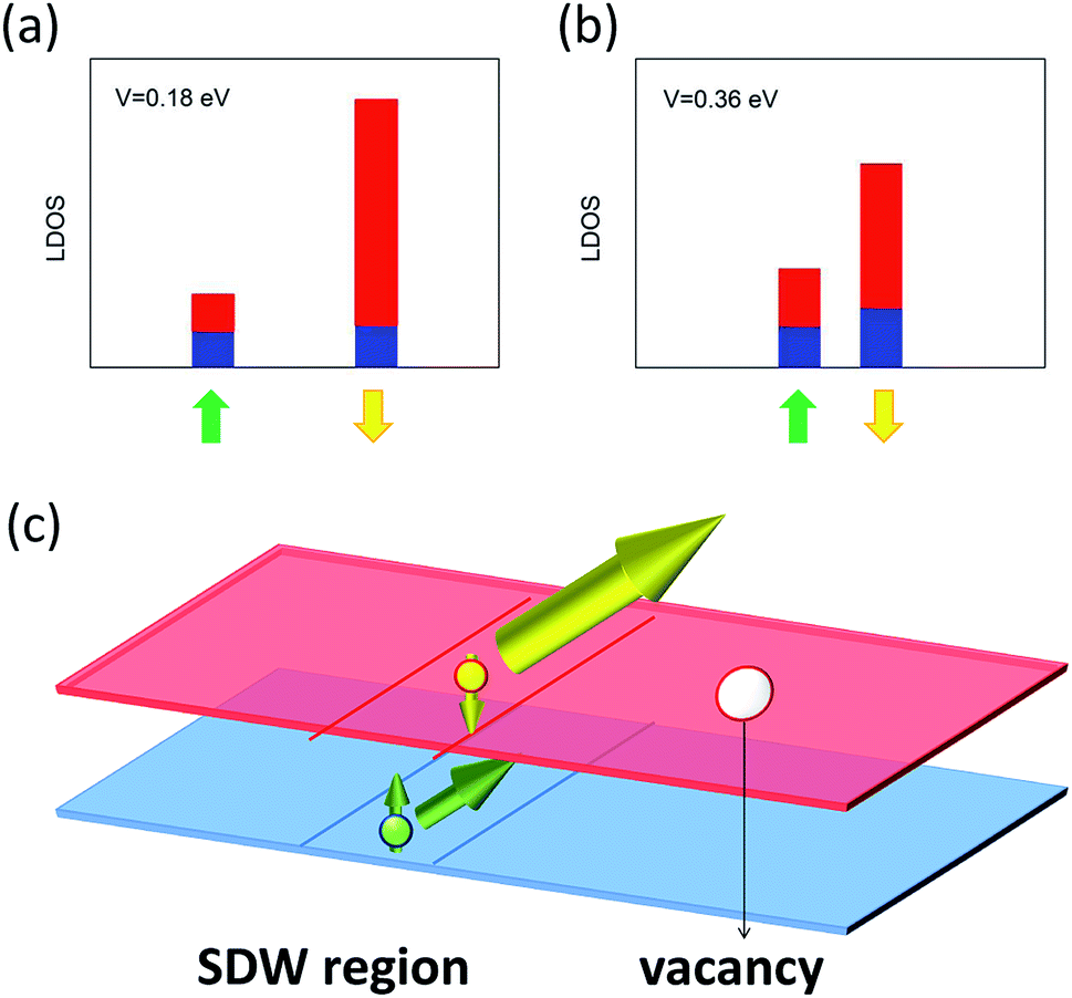 | ||
| Fig. 3 (a) and (b) Layer-resolved LDOS of spin-polarized gapless states shown in Fig. 2 (marked by green and yellow arrows) for the case of BLG with SDW and vacancies for two different gate voltages. Layers are denoted by colours: blue – bottom, red – top. LDOS values are calculated at the Fermi energy and are represented by bar heights. (c) Visualization of current flow along the SDW in BLG with vacancies. The sizes of the dots and arrows represent the current and spin densities, respectively, in the layers. A current with almost fixed spin orientation flows mainly in the upper layer. | ||
The spin polarization of the topological state for experimentally attainable voltages is mainly spin down, and thus almost all the current flow in the SDW will have the same spin orientation mostly localized in one layer, as shown schematically in Fig. 3(c). Therefore, the presence of vacancies in BLG with a SDW affords not only spin splitting of gapless states, but also allows for partial locking of the spin to a single layer. This effect could allow the exploitation of BLG in spintronics and relates to the role of magnetic impurities in general.
Conclusions
We searched for a method to spin split the topologically protected gapless states, which are induced by SDW, that appear in gated BLG to render them useful in spintronic applications. Spin splitting can be accomplished by introducing magnetic defects, which we modelled as π-vacancies. We found that despite the strong perturbation of the topological gapless states caused by the presence of vacancies, a topological state connecting the valence and conduction bands survived in the gap. Its spin degeneracy was lifted, and the state was locked in one graphene layer. We thus obtained two spin-polarized channels for current conductance along the domain wall, which is similar to topological insulators. Although the focus of our study was on vacancies, the results could also be extrapolated to magnetic atoms near a SDW.Conflicts of interest
There are no conflicts to declare.Acknowledgements
This work was partially supported by project FIS2016-76617-P of the Spanish Ministry of Economy and Competitiveness MINECO, the Basque Government under the ELKARTEK project (SUPER), and the Gobierno Vasco-UPV/EHU (Grant No. IT1246-19). AA and WJ acknowledge the hospitality of the Institute of Physics at Nicolaus Copernicus University and the Donostia International Physics Center, respectively.Notes and references
- K. S. Novoselov, A. K. Geim, S. V. Morozov, D. Jiang, Y. Zang, S. V. Dubonos, I. V. Grigorieva and A. A. Firsov, Science, 2004, 306, 666–669 CrossRef CAS PubMed.
- K. S. Novoselov, A. K. Geim, S. V. Morozov, D. Jiang, M. I. Katsnelson, I. V. Grigorieva, S. V. Dubonos and A. A. Firsov, Nature, 2005, 438, 197–200 CrossRef CAS PubMed.
- Y. Cao, Y. Cao, V. Fatemi, S. Fang, K. Watanabe, T. Taniguchi, E. Kaxiras and P. Jarillo-Herrero, Nature, 2018, 556, 43 CrossRef CAS PubMed.
- Y.-M. Lin and P. Avouris, Nano Lett., 2008, 8, 2119–2125 CrossRef CAS PubMed.
- F. Schwierz, Nat. Nanotechnol., 2010, 5, 487–496 CrossRef CAS PubMed.
- S.-M. Choi, S.-H. Jhi and Y.-W. Son, Nano Lett., 2010, 10, 3486–3489 CrossRef CAS PubMed.
- F. Xia, D. B. Farmer, Y. Lin and P. Avouris, Nano Lett., 2010, 10, 715–718 CrossRef CAS PubMed.
- J. E. Padilha, M. P. Lima, A. J. R. da Silva and A. Fazzio, Phys. Rev. B, 2011, 84, 113412 CrossRef.
- H. Santos, A. Ayuela, L. Chico and E. Artacho, Phys. Rev. B, 2012, 85, 245430 CrossRef.
- Q. Zhang, Y. Yaofeng, K. S. Chan, Z. Mu and J. Li, Appl. Phys. Express, 2018, 1, 075104 CrossRef.
- T. Ohta, A. Bostwick, T. Seyller, K. Horn and E. Rotenberg, Science, 2006, 313, 951–954 CrossRef CAS PubMed.
- E. V. Castro, K. S. Novoselov, S. V. Morozov, N. M. R. Peres, J. M. B. L. dos Santos, J. Nilsson, F. Guinea, A. K. Geim and A. H. C. Neto, Phys. Rev. Lett., 2007, 99, 216802 CrossRef PubMed.
- Y. Zhang, T.-T. Tang, C. Girit, Z. Hao, M. C. Martin, A. Zettl, M. F. Crommie, Y. R. Shen and F. Wang, Nature, 2009, 459, 820 CrossRef CAS PubMed.
- B. N. Szafranek, D. Schall, M. Otto, D. Neumaier and H. Kurz, Appl. Phys. Lett., 2010, 96, 112103 CrossRef.
- J. S. Alden, A. W. Tsen, P. Y. Huang, R. Hovden, L. Brown, J. Park, D. A. Muller and P. L. McEuen, Proc. Natl. Acad. Sci., 2013, 110, 11256 CrossRef CAS PubMed.
- A. Vaezi, Y. Liang, D. H. Ngai, L. Yang and E.-A. Kim, Phys. Rev. X, 2013, 3, 021018 Search PubMed.
- P. San-Jose, R. V. Gorbachev, A. K. Geim, K. S. Novoselov and F. Guinea, Nano Lett., 2014, 14, 2052–2057 CrossRef CAS PubMed.
- M. Pelc, W. Jaskolski, A. Ayuela and L. Chico, Phys. Rev. B, 2015, 92, 085433 CrossRef.
- P. Maher, C. R. Dean, A. F. Young, T. Taniguchi, K. Watanabe, K. L. Shepard, J. Hone and P. Kim, Nat. Phys., 2013, 9, 154–158 Search PubMed.
- F. Zhang, A. H. MacDonald and E. J. Mele, Proc. Natl. Acad. Sci. U. S. A., 2013, 110, 10546 CrossRef CAS PubMed.
- L. Ju, Z. Shi, N. Nair, Y. Lv, C. Jin, J. Velasco Jr, C. Ojeda-Aristizabal, H. A. Bechtel, M. C. Martin, A. Zettl, F. Analytis and J. Wang, Nature, 2015, 520, 650–655 CrossRef CAS PubMed.
- J. Li, K. Wang, K. J. McFaul, Z. Zern, Y. Ren, K. Watanabe, T. Taniguchi, Z. Qiao and J. Zhu, Nat. Nanotechnol., 2016, 11, 1060–1065 CrossRef CAS PubMed.
- J. Lin, W. Fang, W. Zhou, A. R. Lupini, J. C. Idrobo, J. Kong, S. J. Pennycook and S. T. Pantelides, Nano Lett., 2013, 13, 3262–3268 CrossRef CAS PubMed.
- W. Jaskólski, M. Pelc, L. Chico and A. Ayuela, Nanoscale, 2016, 8, 6079–6084 RSC.
- W. Jaskólski, M. Pelc, W. G. Bryant, L. Chico and A. Ayuela, 2D Materials, 2018, 5, 025006–026016 CrossRef.
- E. H. Lieb, Phys. Rev. Lett., 1989, 62, 1201 CrossRef PubMed.
- E. J. G. Santos, D. Sanchez-Portal and A. Ayuela, Phys. Rev. B, 2010, 81, 125433–125439 CrossRef.
- E. J. G. Santos, A. Ayuela and D. Sanchez-Portal, New J. Phys., 2012, 14, 043022 CrossRef.
- V. M. Pereira, F. Guinea, J. M. B. Lopes dos Santos, N. M. R. Peres and A. H. Castro Neto, Phys. Rev. Lett., 2006, 96, 036801 CrossRef PubMed.
- J. J. Palacios, J. Fernandez-Rossier and L. Brey, Phys. Rev. B, 2008, 77, 195428 CrossRef.
- M. P. Lopez-Sancho, F. de Juan and M. A. H. Vozmediano, Phys. Rev. B, 2009, 79, 075413 CrossRef.
- K. Kusakabe, Carbon-based magnetism, Elsevier, Amsterdam, 2006, p. 305 Search PubMed.
- W. Jaskólski, A. Ayuela, M. Pelc, H. Santos and L. Chico, Phys. Rev. B, 2011, 83, 235424 CrossRef.
- S. Dutta and K. Wakabayashi, Sci. Rep., 2015, 5, 11744 CrossRef PubMed.
- J. Mao, Y. Jiang, D. Moldovan, G. Li, K. Watanabe, T. Taniguchi, M. R. Masir, F. M. Peeters and E. Y. Andrei, Nat. Phys., 2016, 12, 545 Search PubMed.
- Y. Zhang, S.-Y. Li, H. Huang, W.-T. Li, J.-B. Qiao, W.-X. Wang, L.-J. Yin, K.-K. Bai, W. Duan and L. He, Phys. Rev. Lett., 2016, 117, 166801 CrossRef PubMed.
- T. M. L. Lane, M. Andelkovic, J. R. Wallbank, L. Covaci, F. M. Peeters and V. I. Falko, Phys. Rev. B, 2018, 97, 045301 CrossRef CAS.
- M. B. Nardelli, Phys. Rev. B, 1999, 60, 7828–7833 CrossRef CAS.
- S. Datta, Electronic Transport in Mesoscopic Systems, Cambridge University Press, Cambridge, 1995 Search PubMed.
- L. Chico, L. X. Benedict, S. G. Louie and M. L. Cohen, Phys. Rev. B, 1996, 54, 2600–2606 CrossRef CAS PubMed.
- W. Jaskólski and L. Chico, Phys. Rev. B, 2005, 71, 155405 CrossRef.
- D. Gunlycke, D. A. Areshkin, J. Li, J. W. Mintmire and C. T. White, Nano Lett., 2007, 7, 3608–3611 CrossRef CAS PubMed.
- W. Jaskolski, L. Chico and A. Ayuela, Phys. Rev. B, 2015, 91, 165427 CrossRef.
- M. P. Lopez-Sancho, J. M. Lopez-Sancho and J. Rubio, J. Phys. F: Met. Phys., 1985, 15, 851 CrossRef.
- Smaller spin-splitting for V > γ1 causes less assymetric distribution of LDOS and spins between the layers. This is also true for other cases leading to smaller splitting, like sparse distribution of vacancies or their location away from SDW..
Footnote |
| † Electronic supplementary information (ESI) available. See DOI: 10.1039/c9ra07319a |
| This journal is © The Royal Society of Chemistry 2019 |