DOI:
10.1039/C9RA06976C
(Paper)
RSC Adv., 2019,
9, 32066-32071
Optimization of the electron transport in quantum dot light-emitting diodes by codoping ZnO with gallium (Ga) and magnesium (Mg)†
Received
2nd September 2019
, Accepted 29th September 2019
First published on 9th October 2019
Abstract
In our study, to optimize the electron–hole balance through controlling the electron transport layer (ETL) in the QD-LEDs, four materials (ZnO, ZnGaO, ZnMgO, and ZnGaMgO NPs) were synthesized and applied to the QD-LEDs as ETLs. By doping ZnO NPs with Ga, the electrons easily inject due to the increased Fermi level of ZnO NPs, and as Mg is further doped, the valence band maximum (VBM) of ZnO NPs deepens and blocks the holes more efficiently. Also, at the interface of QD/ETLs, Mg reduces non-radiative recombination by reducing oxygen vacancy defects on the surface of ZnO NPs. As a result, the maximum luminance (Lmax) and maximum luminance efficiency (LEmax) of QD-LEDs based on ZnGaMgO NPs reached 43![[thin space (1/6-em)]](https://www.rsc.org/images/entities/char_2009.gif) 440 cd m−2 and 15.4 cd A−1. These results increased by 34%, 10% and 27% for the Lmax and 450%, 88%, and 208% for the LEmax when compared with ZnO, ZnGaO, and ZnMgO NPs as ETLs.
440 cd m−2 and 15.4 cd A−1. These results increased by 34%, 10% and 27% for the Lmax and 450%, 88%, and 208% for the LEmax when compared with ZnO, ZnGaO, and ZnMgO NPs as ETLs.
Introduction
Excellent properties of colloidal quantum dots (QDs) such as accurate color saturation, easy tunable wavelength, high photoluminescence (PL) efficiency, and good stability have steadily led to a wide range of studies of QD-based light emitting diodes (LEDs) as a prominent candidate for next-generation displays.1–3 The performance of QD-LEDs strongly depends on the device's electron–hole balance, which promotes the utilization of inorganic materials for the electron transport layer (ETL) to minimize the asymmetry of the electron–hole balance.4–6
The ETL of ZnO nanoparticles (NPs) was suggested in preceding studies because of their excellent electron mobility, proper energy band gap, ease of production using simple synthesis methods and ease of deposition. Properties of QD-LEDs with a ZnO NPs ETL are limited by intrinsic defects such as Zn interstitial (Zni) and/or oxygen vacancy (VO), and low valence energy level although enhancement was reported in previous studies.9 The defects easily quench excitons at the ZnO NPs/QDs interface because the charge transfer between the interfaces is disturbed and non-radiative recombination takes place.7,8 The low valence energy level of un-doped ZnO restrains the performance of QD-based LEDs due to lack of sufficient hole blocking at the deep valence energy level of QDs.9
To address this problem, Yang et al.10 proposed doping ZnO NPs with an inorganic II-element, Mg, which effectively improved the charge balance and inhibited exciton quenching of the QD-LEDs. The conduction band minimum (CBM) energy levels of Mg-doped ZnO NPs was systematically closer to the vacuum level with increasing Mg content.6 Ga also attenuated the charge transfer at the interface between Ga-doped ZnO NPs/QDs because the Fermi level of ZnO NPs was increased by the (increment of) Ga dopants.5 However, these studies were also not sufficient to promote charge transfer in QD-LEDs, indicating that a single dopant is not effective.
Herein, we propose multiple dopants to optimize the electron–hole balance through controlling ETL in the QD-LEDs. Ga–Mg-codoped ZnO NPs were synthesized and applied to QD-LEDs in comparison with ZnO-, ZnGaO (ZGO)-, and ZnMgO (ZMO)-based QD-LEDs. Fundamental properties of ZnGaMgO (ZGMO) based QD-LEDs were studied to optimize the charge balance, followed by the discussion about roles of each doping elements in terms of the band theory. When Ga is doped into ZnO NPs, the Fermi level of ZnO increases, thereby making the injection of electrons easier. In addition, Mg codoping deepens the valence band maximum (VBM) and block hole migration more efficiently. As a consequence, by codoping Ga and Mg elements (10% Ga and 3% Mg) into ZnO NPs to optimize the charge balance of the QD-LEDs. The performance of QD-LEDs with ETL consisting of ZGMO NPs indicated a maximum luminance (Lmax) of 43440 cd m−2 at 7 V and a maximum luminance efficiency (LEmax) of 15.4 cd A−1 at 4.5 V. In addition, when applying ZnO, ZGO, and ZMO as ETL to QD-LEDs, the Lmax was 32480 (@ 7 V), 39630 (@ 7 V), and 34090 (@ 7 V) cd m−2, respectively, and the max. LE was respectively 2.8 (@ 4.5 V), 8.2 (@ 5 V), and 5.0 (@ 5.5 V) cd A−1. When these results comparing these results with the results of ZGMO as ETL, the Lmax is increased by 34%, 10%, and 27%, respectively, while LEmax is increased by 450%, 88% and 208%, respectively.
Experimental procedure
Chemicals
Zinc acetate (Zn(CH3COO)2), magnesium acetate tetrahydrate (Mg(CH3COO)2·4H2O), gallium(III) triacetate (Ga(CH3COO)3), dimethyl sulfoxide (DMSO), and tetramethylammonium hydroxide (TMAH) were purchased from Sigma-Aldrich. Poly(3,4-ethylenedioxythiophene):polystyrene sulfonate (PEDOT:PSS, AI 4083) was purchased from Heraeus. Poly(N,N′-bis(4-butylphenyl)-N,N′-bis(phenyl)benzidine) (poly-TPD) was purchased from American Dye Source (ADS), Inc. Alloyed CdSe/ZnS QDs (Green QDs) were purchased from ZEUS Ltd.
Synthesis of ZnO, ZnGaO, ZnMgO, and ZnGaMgO NPs
ZnO NPs were synthesized using the precipitation-solution method as reported in our previous work.11 TMAH (0.9062 g) was completely dissolved in 10 ml of ethanol at room temperature. Then, the solution was slowly injected into a 30 ml DMSO dissolved in zinc acetate (0.5503 g) for 1 h with a magnetic stirrer. Finally, the resultant ZnO NPs were washed with acetone and dispersed in ethanol (∼30 mg ml−1). The above procedure was repeated for the synthesis of ZnGaO (gallium(III) triacetate, 0.1 mmol), ZnMgO (magnesium acetate tetrahydrate, 0.13 mmol), and ZnGaMgO (gallium(III) triacetate, 0.1 mmol and magnesium acetate tetrahydrate, 0.04 mmol) using the appropriate stoichiometry.
Fabrication of QD-LEDs device
QD-LED devices were fabricated on patterned indium-tin-oxide (ITO) glass substrates. The substrates were ultrasonic-cleaned using acetone, ethanol, and deionized water for 15 min and then treated with ultraviolet (UV)–ozone for 15 min. PEDOT:PSS was spin-coated on the ITO glass substrates at 4000 rpm for 40 s and baked at 130 °C for 30 min. The ITO glass substrates were transferred to a nitrogen glove box where the remaining fabrication steps were carried out. Poly-TPD was spin-coated on top of PEDOT:PSS layer at 5000 rpm for 40 s and annealed at 130 °C for 30 min, followed by spin-coating of Green QD layer on the top of it and subsequent annealing at 90 °C for 30 min. ETL of ZnO, ZGO, ZMO, ZGMO NPs were deposited on the Green QD layer using spin-coating technique at 3000 rpm for 40 s and baked at 140 °C for 30 min. Finally, an Al cathode film (120 nm) was deposited by thermal evaporation through a patterned shadow mask.
Fabrication of QD-LEDs device
Synthesized ZnO, ZnGO, ZMO, and ZGMO were analysed using the following characterization techniques: the physical properties (structure and particle morphology) were measured with XRD (RIGAKU D/Max 2500, Cu Kα, λ = 0.154 nm) and TEM (TITAN (TM80-300)). The optical properties were measured with a PerkinElmer Lambda 750 UV/VIS/NIR spectrometer and Jasco FP-8500 Spectrofluorometer. The surface chemical composition and binding energy of the constitutional elements were examined by the X-ray Photoelectron Spectroscopy (XPS) (ULVAC PHI 5000 Versa Probe system, Al Kα, hv = 1486.6 eV). The Fermi level and work function of the ZnO NPs were determined utilizing ultraviolet photoelectron spectroscopy (UPS) (ULVAC PHI 5000 Versa Probe, helium discharge lamp, hν = 21.22 eV). The current–voltage–luminance characteristics of the devices were measured with a Spectra Scan PR-670 spectroradiometer and a Keithley-2400 source-measure unit.
Results and discussion
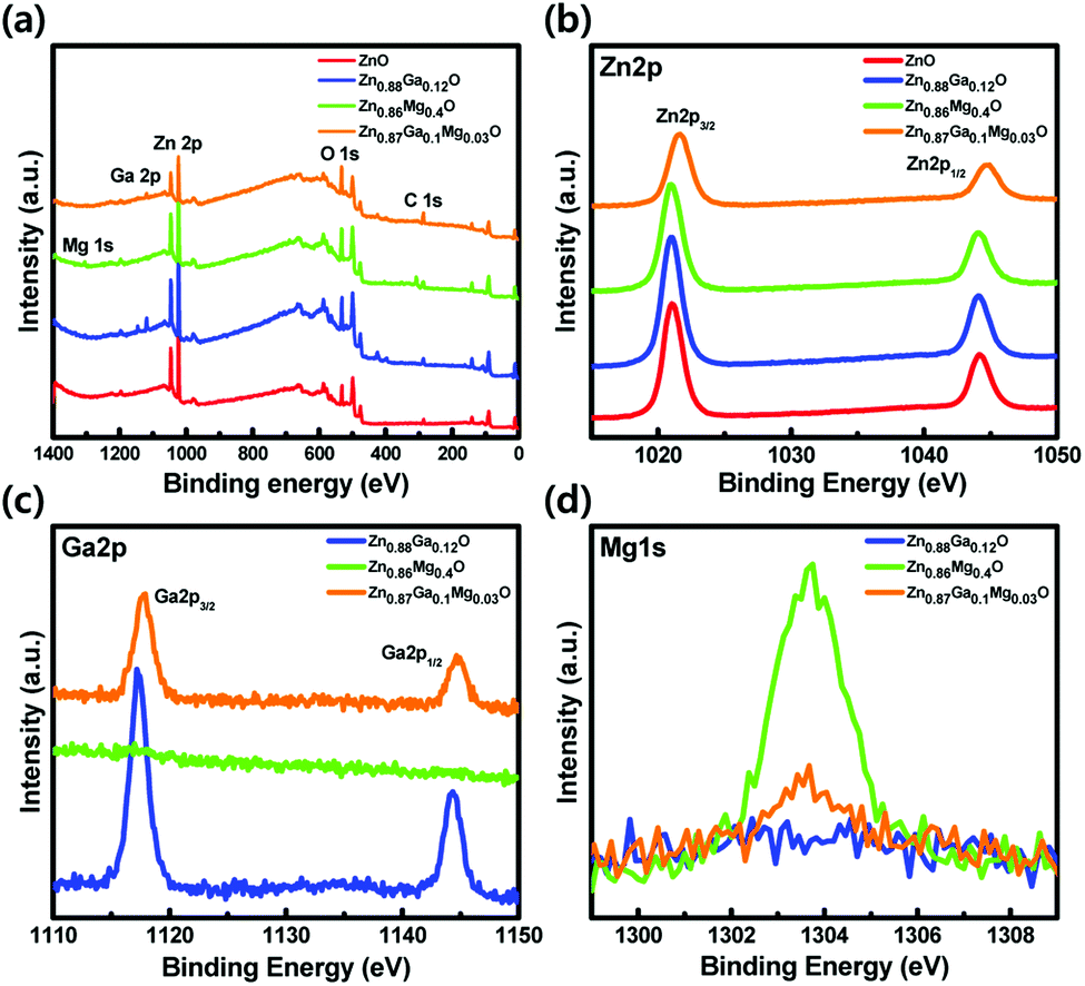
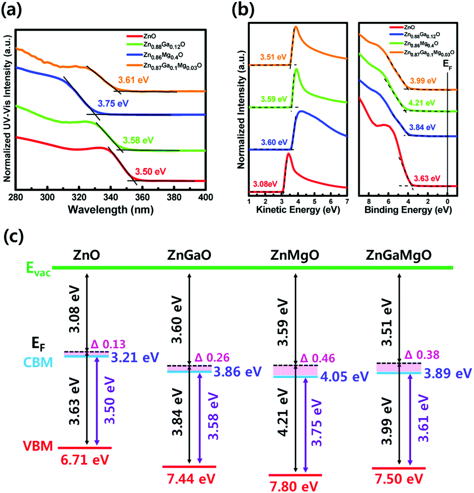
QD-LEDs with various concentrations were fabricated to control the energy level of ETL in the QD-LEDs. XPS results in Table 1 (see the ESI†) confirmed the relative atomic ratio between the elements of each specimen: ZnO, Zn0.88Ga0.12O, Zn0.86Mg0.14O, and Zn0.87Ga0.1Mg0.03O, indicating that Ga and/or Mg were successfully incorporated into ZnO NPs. The XRD results of ZnO, ZGO, ZMO, and ZGMO NPs in Fig. 1(a) clearly showed peaks of a wurtzite hexagonal ZnO structure: (100), (002), (101), (102), (110), (103), and (112), ruling out the formation of phase-separated corundum type Ga2O3 and cubic MgO. All the other observed XRD peaks were weak and broad with increasing doping ratio of Ga and/or Mg, suggesting that the particle sizes of ZGO and ZMO, and ZGMO NPs are smaller than those of ZnO. The XRD peak broadening is therefore the result of the nano-size effect.12Fig. 1(b)–(d) show characteristic transmission electron microscopy (TEM) and high-resolution TEM (HRTEM) images of ZnO, ZnGaO, ZnMgO, and ZnGaMgO NPs. As shown in the insets, the inter-planar spacings of 0.25 nm and 0.27 nm of crystal lattice fringes correspond to (100) lattice plane of ZnO NPs,13 which is inconsistent with any inter-planar spacing of Ga2O3 or MgO (slightly different to each other. Additional information is available in Fig. S1, ESI†). Since the radii of Ga3+ (0.62 Å) and Mg2+ (0.74 Å) are similar to that of Zn2+ (0.72 Å),14 Ga and Mg doping results in the formation of substitutional solid reaction without appreciable strain and thus only slightly increase and decrease of inter-planar spacing, respectively. This is consistent with the previous observation that the covalent bond length of Ga–O (1.92 Å) is more slightly shorter and that of Mg–O (2.06 Å) is more slightly longer than that of Zn–O (1.97 Å). However, the reason for this is not clear yet and further investigation is necessary. Fig. 2 shows XPS spectra of ZnO, ZGO, ZMO, and ZGMO NPs that also confirm the presence of Zn, Ga, and Mg elements in the NPs. Fig. 2(b) presents the high-resolution Zn 2p XPS spectra of each phase. As for ZnO NPs, the two peaks measured at 1044.41 eV and 1021.32 eV are attributed to the spin–orbit splitting (ΔESO = 23.09 eV) of Zn 2p1/2 and Zn 2p3/2 core levels, respectively. Zn 2p1/2 and Zn 2p3/2 peaks of ZGO, ZMO, and ZGMO NPs are 1044.46 eV, 1044.62 eV, 1045.01 eV and 1021.38 eV, 1021.51 eV, and 1021.93 eV, respectively and their ΔESO's are almost the same. The observed Zn 2p peak shifted toward slightly higher binding energies of doped ZnO NPs and this is believed to be a result of the replacement of Zn2+ by Ga3+ and/or Mg2+.15,16 The known electronegativity values of Mg, Zn, Ga, and O atoms are 1.35, 1.65, 1.81, and 3.44, respectively. In the case of ZMO NPs, even though relative difference of electronegativity between Zn and O (3.44–1.65) is smaller than that between Mg and O (3.44–1.35), the relaxation of Mg–O bonding distance up to 2.06 Å longer than Zn–O (1.97 Å) in Zn–O–Mg makes Zn less electronegative than Zn in Zn–O–Zn. This clearly confirms the shifting of the Zn 2p XPS peak toward higher binding energy. On the contrary, relative difference of electronegativity between Zn and O (3.44–1.65) is larger than that between Ga and O (3.44–1.81), but the contraction of Ga–O bonding down to 1.92 A shorter than Zn–O (1.97 A) in Zn–O–Ga also makes Zn less electronegative than Zn in Zn–O–Zn, which further explains the shifting of the Zn 2p to higher energy values. In other words, it can be said that the shifting of the Zn 2p peak is partly effected by the formation of Zn–O–Ga and/or Zn–O–Mg bonds.17,18Fig. 2(c) and (d) show the high-resolution Ga 2p and Mg 1s XPS spectra of ZGO, ZMO, and ZGMO NPs. The Ga 2p peaks of ZGO NPs detected at 1144.37 eV and 1117.42 eV are due to the spin–orbit splitting (ΔESO = 26.95 eV) of Ga 2p1/2 and Ga 2p3/2 core levels, respectively. A Ga 2p peak shifts to slightly higher binding energy in ZGMO NPs and this was presumably due to Mg2+ substitution in Zn–O–Ga–O–Mg bonds where longer distance of Mg–O than Zn–O in ZGMO makes Ga less electronegative than Ga in ZnGaO. However, no remarkable shift of Mg 1 s peak was observed between ZMO and ZGMO. As shown in Fig. 3, the O 1s peak for ZnO NPs was resolved into three OI (529.6 eV), OII (530.7 eV), and OIII (531.8 eV) subpeaks corresponding to O2− ions on the wurtzite structure of the Zn2+ ion array Zn–O, oxygen vacancy, and surface oxygen like –OH respectively.9,19,20 Relative OII ratio decreases by 37.26%, 11.46%, 14.5%, and 3.03% in ZnO, ZMO, ZGO, and ZGMO NPs respectively, which indicates the reduction of oxygen vacancy defects participating in non-radiative recombination at the interface of ODs/ETLs. Upon Ga and/or Mg doping, a slight shift toward higher O 1s binding energies of 529.7 eV for ZGO and ZMO, and 530.1 eV for ZGMO can be ascribed to the added contribution from Zn–O–Mg (530.2 eV) and Mg–O (530.5–530.8 eV) bonds.21,22 In Fig. 4(a), the normalized absorbance spectra in UV and visible light region of ZGO, ZMO, and ZGMO NPs are distinctive from ZnO NPs. According to the results obtained, the optical band gaps were calculated to be approximately 3.50 eV, 3.58 eV, 3.75 eV, and 3.61 eV in ZnO, ZGO, ZMO, and ZGMO NPs, respectively. The band gaps of all doped NPs increases compared to that of un-doped ZnO NPs whereas the band gap of ZMO NPs is the highest, confirming that impurity doping in ZnO NPs results in a blue shift. When Ga and Mg are co-doped in ZnO NPs, the band gap value obtained is between the band gap values of ZGO and ZMO NPs. Fig. 4(b) shows the UPS spectra of the valence band edge and secondary electron cut-off regions of ZnO, ZGO, ZMO, and ZGMO NPs films. The work functions (WFs) are calculated from the difference between the incident photon energy (hv = 21.22 eV) and the high binding energy cut-off (Eoff). The WFs were approximately measured to be 3.08 eV, 3.60 eV, 3.59 eV, and 3.51 eV, respectively, indicating that WFs in our specimens are much lower than that of typical ZnO films, ∼5.2 eV.23,24 This demonstrates that the Fermi levels are higher than the conduction band minimum (CBM) energy as high as 0.13–0.38 eV and confirms that electronic energy levels are degenerate. The widening of the bandgap in the degenerated semiconductor has been observed and well explained by the Burstein–Moss (BM) shift equation.25 The donor concentration (ND) of four materials calculated using the BM shift eqn (1) are: 1.76 × 1019 cm−3, 4.99 × 1019 cm−3, 1.17 × 1020 cm−3 and 8.83 × 1019 cm−3 (see the BM shift eqn (1), ESI†). An increase/decrease of ND with different doping ratios are attributed to intrinsic defects (oxygen vacancy or Zn interstitial) or impurity defects (Ga and/or Mg elements) varied from un-doped ZnO NPs. The valence band maximum's (VBMs) for each material are approximately estimated as 6.71 eV, 7.44 eV, 7.80 eV, and 7.50 eV from the vacuum level. Fig. 4(c) shows the energy band level alignments of four materials with different doping conditions. The optical band gap analyzed in Fig. 4(a) is used to determine the conduction band minimum (CBM). As mentioned in the introduction, the VBM of ZnO NPs is similar to that of green QDs so that ZnO NPs are not likely to act as hole blocking layer (HBL). Furthermore, injection of electrons from the Al cathode (4.3 eV) into the ETL is constrained since the CBM of ZnO NPs is as low as 3.21 eV. The energy band level alignments in Fig. 4(c) apparently present that when Ga and Mg are doped into ZnO NPs an injection barrier for electrons between CBM of ETL and Al becomes quite smaller as 0.25–0.44 eV than 1.09 eV in ZnO ETL and the hole blocking barrier between VBM of ETL and VBM of QDs also increases up to 0.94–1.3 eV from 0.21 eV in ZnO ETL and thus effectively blocks holes for charge balance mechanism. Thus, the suggestion in this study could be confirmed to improve the charge recombination efficiency in QD-LEDs. Fig. 5(a) shows a schematic of a fabricated LED device with a typical structure of patterned ITO (anode)/PEDOT:PSS as hole injection layer (HIL)/poly-TPD (HTL)/green QDs as emissive layer (EML)/ZnO, ZGO, ZMO, or ZGMO NPs (ETL or HBL)/Al (cathode). Fig.
5(b)–(e) show energy band diagrams, current density–voltage, luminance, current efficiency (cd A−1), and power efficiency (lm W−1) respectively, of the QD-LEDs device based on ZnO, ZGO, ZMO, and ZGMO NPs. From Fig. 5(b), three kinds of the energy offset (ΔG) can be considered and are listed in Table 2.† First, an injection barrier (ΔGIn = CBMETL/Al) at the interface between ETLs and Al electrode, caused by Schottky contact decreases from 1.09 eV for ZnO to 0.25 eV for ZGMO. The larger ΔGIn, the more improved charge balance and reduced non-radiative Auger recombination. Second, a conduction band offset (ΔGCBM) between the CBM's of ETL and QDs. ΔGCBM is varied from 0.99 eV to 0.15 eV, which is related to spontaneous electron transfer rate from QDs to ETLs and efficiency. These results verify that the Ga and Mg doping of the ZnO NP ETL helps to maintain the charge neutrality of the QD emitters and to preserve their superior emissive properties. Third, there isa valence band offset (ΔGVBM) between the VBM's of ETLs and QDs. ΔGVBM increases from 0.21 eV for ZnO to 1.30 for ZMO ETLs. The deeper ΔGVBM will effectively confine hole in QDs and thus enhance the charge recombination efficiency. The current density–voltage (J–V) characteristics in Fig. 5(c) exhibit that the QD-LEDs with ZGO, ZMO, and ZGMO NPs have a lower turn-on voltage of 4.0–4.5 V than 5 V of ZnO and the lower current density. Moreover, when dopants are added into ZnO NPs ETL in QD-LEDs luminance, current efficiency, and power efficiency characteristics are more improved compared with un-doped ZnO NPs. As shown in Fig. 5(d) and (e), the device with the ZGMO NPs ETL displays the maximum values of luminance of 43440 cd m−2 at 7 V, current efficiency of 15.4 cd A−1 at 4.5 V, and power efficiency of 10.3 lm W−1, which increased by 34% (luminance), 450% (current efficiency), and 470% (power efficiency) compared to those of the device with the ZnO NPs ETL (32480 cd m−2 at 7 V, 2.8 cd A−1, 4.5 V, and 1.8 lm W−1). In terms of luminance, current efficiency, and power efficiency results, the barrier heights of ΔGCBM = 0.31 eV and ΔGCBM = 1.0 eV in ZGMO are believed to be the most optimum condition for charge neutrality of QDs for a facilitative electron injection at interface of ETL/Al and an effectively limited hole migration. The inset in Fig. 5(d) presents an emission photographic image of QD-LEDs based on the ZGMO NPs as ETL, acquired at a voltage of 6 V. To reduce non-radiative recombination and increase the device efficiency, it is critical to engineer the charge transport layers to achieve balanced charge transport and low leakage currents.26–28 In order to confirm the charge transfer effect of doped Ga and/or Mg elements in ZnO NPs on electron-only devices, devices of ITO/ETL (ZnO, ZGO, ZMO, and ZGMO NPs)/green QDS/ETL (ZnO, ZGO, ZMO, and ZGMO NPs)/Al were fabricated as shown in Fig. 6(a). As shown in Fig. 6(b) it is revealed that current density decreases as Ga and Mg elements are incorporated and shows the lowest value in the QD-LEDs with ZGMO ETLs. It is well known that the conductivity of ZnO depends on the concentration of oxygen vacancies, because oxygen vacancies can help improve the electron mobility.29,30 Therefore, these results confirm that the incorporation of Ga, Mg dopants into ZnO NP ETLs is an effective means of reducing non-radiative charge recombination and consequently, enhancing the efficiency of QD-LED devices. This result indicates that the conductivity of ZGMO is lower than that of the other ZGO and ZMO ETL materials.
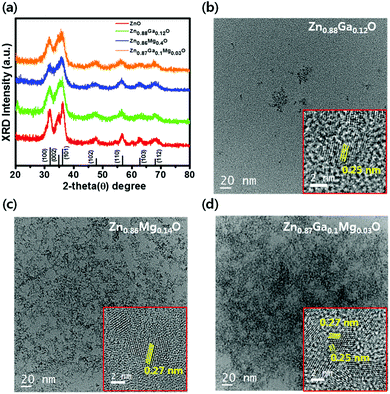 |
| | Fig. 1 (a) XRD patterns of ZnO, ZnGaO, ZnMgO, and ZnGaMgO. (b), (c), and (d) TEM images of ZnGaO, ZnMgO, and ZnGaMgO, respectively. The insets in (b, c, and d) show the HRTEM images and crystal lattice planes with d-spacing. | |
 |
| | Fig. 2 XPS spectra of ZnO, ZnGaO, ZnMgO, and ZnGaMgO (a) full range XPS spectra (b) XPS spectra of Zn 2p core-level, (c) Ga 2p core-level, and (d) Mg 1s core-level. | |
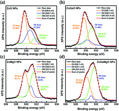 |
| | Fig. 3 O 1s core level XPS spectra of (a) ZnO, (b) ZnGaO, (c) ZnMgO, and (d) ZnGaMgO NPs. | |
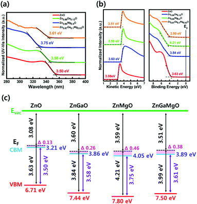 |
| | Fig. 4 (a) Normalized UV-Vis absorption spectra of ZnO, ZnGaO, ZnMgO, ZnGaMgO NPs depending on the ratio of each element, respectively. (b) The valence band edge regions and the secondary electron cut-off region via UPS spectra, and (c) corresponding electronic energy level diagrams. | |
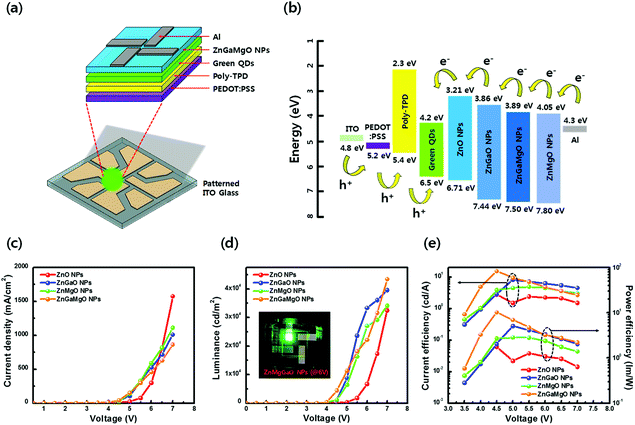 |
| | Fig. 5 (a) Schematic 3-dim device structure and (b) flat-band energy diagram of the QD-LEDs device based on ZnO, ZnGaO, ZnMgO, and ZnGaMgO NPs. For QD-LEDs with four different ETLs, (c) current density versus voltage, (d) luminance versus voltage, and (e) current efficiency and power efficiency versus voltage curves. | |
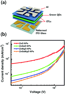 |
| | Fig. 6 (a) A schematic image of an electron-only QD-LEDs using a ZnO, ZnGaO, ZnMgO, and ZnGaMgO NPs as ETLs and (b) their characteristic current density–voltage (J–V) curves. | |
Conclusions
In conclusion, we have optimized electron–hole balance of QD-LEDs by using Ga–Mg-codoped ZnO NPs as ETL. The Ga–Mg-codoped ZnO NPs improved charge balance and reduced non-radiative Auger recombination in QD-LEDs. In addition, the performance of QD-LEDs is improved by minimizing the oxygen vacancy of ZnO NPs and thus lowering leakage current. As a results, the Lmax and LEmax of QD-LEDs based on ZGMO NPs reach 43440 cd m−2 and 15.4 cd A−1. These results are increased by 34%, 10% and 27% for the Lmax and 450%, 88%, and 208% for the LEmax when compared with ZnO, ZGO, and ZMO NPs as ETL. It is therefore reasonable to conclude that Ga and Mg co-doping of ZnO is more effecting in improving electron transport compared individual doping of Ga and Mg.
Conflicts of interest
There are no conflicts of interest to declare.
Acknowledgements
This work was supported by Korea Institute of Science and Technology (KIST) Institutional Program under Contract No. 2E28200 and South Africa/South Korea joint collaboration programmed managed by National Research Foundation, (Grant No. 2014K1A3A1A09063246/SKO15081792426)
References
- L. Sun, J. J. Choi, D. Stachnik, A. C. Bartnik, B.-R. Hyun, G. G. Malliaras, T. Hanrath and F. W. Wise, Nat. Nanotechnol., 2012, 7, 369 CrossRef CAS.
- K.-H. Lee, J.-H. Lee, W.-S. Song, H. Ko, C. Lee, J.-H. Lee and H. Yang, ACS Nano, 2013, 7, 7295–7302 CrossRef CAS.
- K. Qasim, B. Wang, Y. Zhang, P. Li, Y. Wang, S. Li, S.-T. Lee, L.-S. Liao, W. Lei and Q. Bao, Adv. Funct. Mater., 2017, 27, 1606874 CrossRef.
- L. Wang, J. Pan, J. Qian, W. Lei, Y. Wu, W. Zhang, D. K. Goto and J. Chen, J. Mater. Chem. C, 2018, 6, 8099–8104 RSC.
- S. Cao, J. Zheng, J. Zhao, Z. Yang, C. Li, X. Guan, W. Yang, M. Shang and T. Wu, ACS Appl. Mater. Interfaces, 2017, 9, 15605–15614 CrossRef CAS.
- Y. Sun, Y. Jiang, H. Peng, J. Wei, S. Zhang and S. Chen, Nanoscale, 2017, 9, 8962–8969 RSC.
- K. Tvrdy, P. A. Frantsuzov and P. V. Kamat, Proc. Natl. Acad. Sci. U. S. A., 2011, 108, 29–34 CrossRef CAS.
- W. H. Cheng, J. W. Chiou, M. Y. Tsai, J. S. Jeng, J. S. Chen, S. L. C. Hsu and W. Y. Chou, J. Phys. Chem. C, 2016, 120, 15035–15041 CrossRef CAS.
- Y. J. Lee, H. H. Kim, Y. J. Lee, J. H. Kim, H.-J. Choi and W. K. Choi, Nanotechnology, 2019, 30, 035207 CrossRef CAS.
- J.-H. Kim, C.-Y. Han, K.-H. Lee, K.-S. An, W. Song, J. Kim, M. S. Oh, Y. R. Do and H. Yang, Chem. Mater., 2015, 27, 197–204 CrossRef CAS.
- H. H. Kim, Y. J. Lee, C. Park, S. Yu, S. O. Won, W.-S. Seo, C. Park and W. K. Choi, Part. Part. Syst. Charact., 2018, 1800080 CrossRef.
- H. M. Xiong, D. G. Shchukin, H. Mohwald, Y. Xu and Y. Y. Xia, Angew. Chem., Int. Ed., 2009, 48, 2727–2731 CrossRef CAS.
- X. Liang, Y. Ren, S. Bai, N. Zhang, X. Dai, X. Wang, H. He, C. Jin, Z. Ye, Q. Chen, L. Chen, J. Wang and Y. Jin, Chem. Mater., 2014, 26, 5169–5178 CrossRef CAS.
- R. D. Shannon, Acta Crystallogr., Sect. A: Cryst. Phys., Diffr., Theor. Gen. Crystallogr., 1976, 32, 751 CrossRef.
- C. J. Ku, W. C. Hong, T. Mohsin, R. Li, Z. Q. Duan and Y. C. Lu, IEEE Electron Device Lett., 2015, 36, 914–916 CAS.
- X. Zhang, L. Li, J. Su, Y. Wang, Y. Shi, X. Ren, N. Liu, A. Zhang, J. Zhou and Y. Gao, Laser Photonics Rev., 2014, 8, 429–435 CrossRef CAS.
- M. K. Hamza, J. M. Bluet, K. Masenelli-Varlot, B. Canut, O. Boisron, P. Melinon and B. Masenelli, Nanoscale, 2015, 7, 12030–12037 RSC.
- E. Della Gaspera, A. S. R. Chesman, J. van Embden and J. J. Jasieniak, ACS Nano, 2104, 8, 9154–9163 CrossRef.
- S. S. Hullavarad, N. V. Hullavarad, D. E. Pugel, S. Dhar, T. Venkatesan and R. D. Vispute, Opt. Mater., 2008, 30, 993 CrossRef CAS.
- D. W. Langer and C. J. Vesely, Phys. Rev. B: Solid State, 1970, 2, 4885 CrossRef.
- V. I. Nefeddov, M. N. Firsov and I. S. J. Shaplygin, J. Electron Spectrosc. Relat. Phenom., 1982, 26, 625 Search PubMed.
- A. Le Febvrier, J. Jensen and P. Eklund, J. Vac. Sci. Technol., A, 2017, 35, 021407 CrossRef.
- J. Xiao, X. X. Zhang and G. M. Zhang, Nanotechnology, 2008, 19, 295706 CrossRef.
- J. B. You, X. W. Zhang, P. F. Cai, J. J. Dong, Y. Gao, Z. G. Yin, N. F. Chen, R. Z. Wang and H. Yan, Appl. Phys. Lett., 2009, 94, 262105 CrossRef.
- C. E. Kim, P. Moon, S. Kim, J.-M. Myoung, H. W. Jang, J. Bang and I. Yun, Thin Solid Films, 2010, 518, 6304–6307 CrossRef CAS.
- X. Dai, Z. Zhang, Y. Jin, Y. Niu, H. Cao, X. Liang, L. Chen, J. Wang and X. Peng, Nature, 2014, 515, 96–99 CrossRef CAS PubMed.
- J. Pan, J. Chen, Q. Huang, Q. Khan, X. Liu, Z. Tao, Z. Zhang, W. Lei and A. Nathan, ACS Photonics, 2016, 3, 215–222 CrossRef CAS.
- S. Cao, J. Zheng, J. Zhao, Z. Yang, C. Li, X. Guan, W. Yang, M. Shang and T. Wu, ACS Appl. Mater. Interfaces, 2017, 9, 15605–15614 CrossRef CAS.
- K. Nomura, H. Ohta, A. Takagi, T. Kamiya, M. Hirano and H. Hosono, Nature, 2004, 432, 488 CrossRef CAS PubMed.
- E. Fortunato, P. Barquinha and R. Martins, Adv. Mater., 2012, 24, 2945–2986 CrossRef CAS.
Footnotes |
| † Electronic supplementary information (ESI) available: Additional figure (Fig. S1), text and tables (Tables 1 and 2). See DOI: 10.1039/c9ra06976c |
| ‡ These authors contributed equally. |
|
| This journal is © The Royal Society of Chemistry 2019 |
Click here to see how this site uses Cookies. View our privacy policy here. 
 Open Access Article
 This Open Access Article is licensed under a Creative Commons Attribution-Non Commercial 3.0 Unported Licence
 e,
Cheolmin
Park
e,
Cheolmin
Park