
 Open Access Article
 This Open Access Article is licensed under a Creative Commons Attribution-Non Commercial 3.0 Unported Licence
Observation of giant spin–orbit interaction in graphene and heavy metal heterostructures†
Amir Muhammad
Afzal
,
Kuen Hong
Min
,
Byung Min
Ko
and
Jonghwa
Eom
 *
*
Department of Physics & Astronomy, Graphene Research Institute-Texas Photonics Center International Research Center (GRI-TPC IRC), Sejong University, Seoul 05006, Korea. E-mail: eom@sejong.ac.kr
First published on 7th October 2019
Abstract
Graphene is a promising material demonstrating some interesting phenomena such as the spin Hall effect, bipolar transistor effect, and non-trivial topological states. However, graphene has an intrinsically small spin–orbit interaction (SOI), making it difficult to apply in spintronic devices. The electronic band structure of graphene makes it possible to develop a systematic method to enhance SOI extrinsically. In this study, we designed a graphene field-effect transistor with a Pb layer intercalated between graphene (Gr) and Au layers and studied the effect on the strength of the SOI. The SOI in our system was significantly increased to 80 meV, which led to a giant non-local signal (∼180 Ω) at room temperature due to the spin Hall effect. Further, we extract key parameters of spin transport from the length and width dependence of non-local measurement. To support these findings, we also measured the temperature and gate-dependent weak localization (WL) effect. We obtained the magnitude of the SOI and spin relaxation time of Gr via quantitative analysis of WL. The SOI magnitudes estimated from the non-local signal and the WL effect are close in value. The enhancement of the SOI of Gr at room temperature is a potential simple manipulation method to explore the use of this material for spin-based applications.
Introduction
Graphene (Gr), with its honey-comb structure of carbon atoms, has enormous potential for used in spintronics, electronics, data storage, and information processing devices.1–3 It has become a strong contender for next-generation spin-based devices owing to its high mobility, weak hyperfine coupling, long diffusion length, and gate tuneable spin transport at room temperature.4–6 However, its lack of an intrinsic spin–orbit interaction (SOI) and a bandgap are serious limitations and make it difficult to apply Gr to spintronic devices.7 The SOI in Gr has attracted much theoretical attention to date but is less investigated experimentally.8The decoration of the surface of Gr provides a platform for manipulating its SOI due to its surface sensitivity.9 Different procedures have been proposed to improve the SOI in Gr. For example, the intrinsic SOI of Gr has been enhanced significantly by creating a curve in flat Gr and by carbon nanotubes.10,11 Balakrishnan et al.12 and Avsar et al.13 have, respectively, suggested enhancing the SOI in GR via chemical treatment with 2.5 meV of hydrogen and 5.1–9.1 meV of fluorine. Unfortunately, these chemisorbed light atoms make devices unstable in ambient conditions because these atoms can be easily unglued at moderate temperature.
Zhang et al.14 and Weeks et al.15 proposed a similar approach to enhance SOI in Gr. They recommended depositing heavy metals onto the hollow centre of the honeycomb lattice of the carbon sheet that modified the SOI in Gr and opened a bandgap at the Dirac point. Similarly, Ir and W 5d atoms can intercede in a quantum anomalous Hall state.14 Alternatively, d-block metals such as Au, Ti, and In have strong SOIs and can open a bandgap at the Dirac point in Gr; they can also introduce the quantum spin Hall effect in the Gr sheet.15 4d and 5d heavy transition metals demonstrate intriguing physical properties necessary for spintronics devices, especially when interlinked with a magnetic materials.16,17 Despite these promising applications, one genuine problem that remains is that the surface adsorption induces additional electronics scattering. The coherence of the Dirac fermions can be suppressed by such electronic scattering.14,15,18 Recently, a van der Waals (vdW) heterostructure assembled by vertically staking Gr and two-dimensional materials resulted in a compact system with possibility to manipulate and modulate the spin-based field-effect transport properties. The hybridization of transition metal dichalcogenides (TMDs) or Gr with magnetic materials can strongly modulate the electronic structure via the proximity effect.19–21 However, suggestions for how to begin SOI enhancement in Gr and spin absorption in two-dimensional TMDs are still elusive or remain controversial.22–24 These approaches are responsible for disorders in the charge transport quality and have a number of limitations for spin transport, making it problematic for use in controlling the SOI in Gr. Moreover, an elusive challenge in this field is the realization of enhanced SOI and induced topological nontrivial gaps inside the Dirac point. In this work, we made a Gr/Pb/Au heterostructure field effect transistor (FET). For the first time, we used Pb as an intercalated layer between the graphene and Au and measured SOI in the heterostructure device in local and non-local measurement configurations. Intercalation of the Pb thin layer between Au and Gr leads to significant modification of the electronic structure and SOI of the latter. We observed a giant spin Hall effect (RNL ∼ 180 Ω) in the device without ferromagnetic electrodes. To further quantitatively examine the improvement in the magnitude of SOI of Gr, we fit our magneto-conductivity data to an equation from the theory of weak localization (WL). The SOI values calculated for Gr through non-local configuration and WL analysis are similar, supporting the internal consistency of experimental results in this study. The effective improvement of SOI in the Gr-based system opens a new gateway to explore new areas of the spin FET phenomenon.
Characterization of the SLG/Pb + Au heterostructure device
Fig. 1a is a schematic of the Gr/Pb/Au heterostructure device and Fig. 1b is an optical image of the final device in one of its two basic Hall bar configurations. In one of these configurations, Gr is underneath the Pb and Au; in the other, the Gr does not have any top layers. The Raman spectra of graphene on SiO2 are shown in Fig. S1c,† in which the G and 2D peaks appear around 1580 cm−1 and 2700 cm−1. The ratio of intensities of G and 2D peaks (I2D/IG) is ∼2.6, which is related to a previously reported value of single layer Gr (SLG).25,26 Atomic force microscopy (AFM) was used to confirm the thickness. Fig. S2b† shows the height profile of Gr on SiO2, with the thickness of SLG being ∼0.337 nm.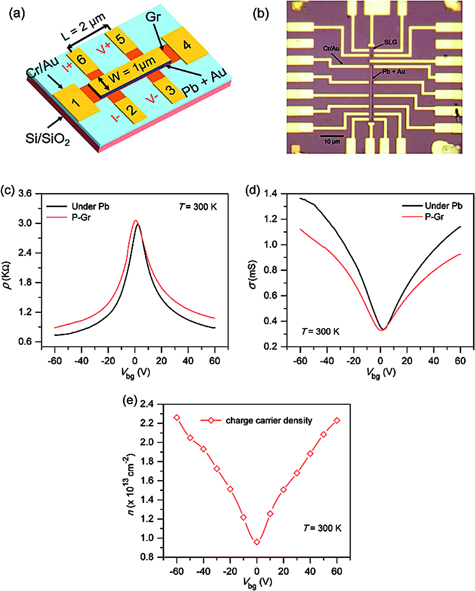 | ||
| Fig. 1 (a) Schematic of graphene (Gr) device for local and non-local configuration with lead (Pb) and without Pb. In non-local measurement, we applied a current between 6 and 2 and perceived the voltage drop between 5 and 3. For local measurement, we applied a current between electrodes 1 and 4 and detected the voltage drop between 2 and 3. In each case, the length and width of the channel is L = 2 μm and W = 1 μm, respectively. (b) Optical image of a completed device with multiple Hall bars on pristine graphene (P-Gr) and graphene with Pb + Au. (c) Resistivity of P-Gr and covered graphene with Pb + Au as a function of back-gate voltages at room temperature. (d) Conductivity of P-Gr and covered graphene as a function of back-gate voltages at room temperature. (e) Charge carrier density as a function of back-gate voltages. | ||
First, the charge transport was characterized. Fig. 1c and d show resistivity and conductivity as a function of back-gate voltage. The back-gate voltage was swept from −60 V to +60 V and resistivity and conductivity were measured. In cases of pristine Gr, the charge neutrality point (CNT) (i.e., the Dirac point) lies nearly at zero back-gate voltage. When Pb is deposited, the Dirac point shifts in a positive direction. The mobility of Gr can be calculated by μ = (1/Cg) (∂σ/∂V), where Cg is the gate capacitance and σ is conductivity. The calculated mobilities are 25![[thin space (1/6-em)]](https://www.rsc.org/images/entities/char_2009.gif) 000 cm2 V−1 s−1 and 29100 cm2 V−1 s−1 in pristine graphene and graphene with Pb + Au, respectively.27–30 Furthermore, we measured the charge carrier density as a function of back-gate voltage at room temperature, as shown in Fig. 1e. For the charge carrier density, we measured the Hall measurement at the different back-gates and calculated charge carrier density using n = 1/(eRxy/B), where Rxy is the Hall resistance at magnetic field B and e is the charge of an electron.
000 cm2 V−1 s−1 and 29100 cm2 V−1 s−1 in pristine graphene and graphene with Pb + Au, respectively.27–30 Furthermore, we measured the charge carrier density as a function of back-gate voltage at room temperature, as shown in Fig. 1e. For the charge carrier density, we measured the Hall measurement at the different back-gates and calculated charge carrier density using n = 1/(eRxy/B), where Rxy is the Hall resistance at magnetic field B and e is the charge of an electron.
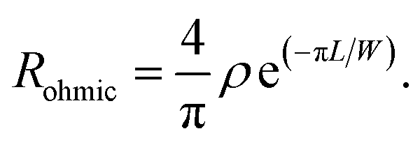
Next, we turned our attention to confirming the origin of the large non-local (NL) signal we obtained; this was done by measuring the NL charge transport. We measured the length (L) and width (W) of the channel-dependent non-local signal to confirm its nature. We studied the length dependence of the non-local signal by keeping width fixed (W = 1 μm) and varying L (2–6 μm). We measured the non-local signal of pristine Gr by applying a constant current (I = 0.99 μA) between two electrodes (6 & 2) and a detected a decrease in voltage (V) across the neighbouring pair of electrodes (5 & 3). The NL signal obtained (RNL ∼ 9.6 Ω) was not very high; it was also comparable in magnitude with the ohmic contribution shown in Fig. 2b. For ohmic measurement, we applied the current between the pair of electrodes (1 & 4) and measured the drop in V between the other pair (2 & 3). The dimensions of the channel are L = 2 μm and W = 1 μm. The ohmic leakage contribution is calculated using the following:
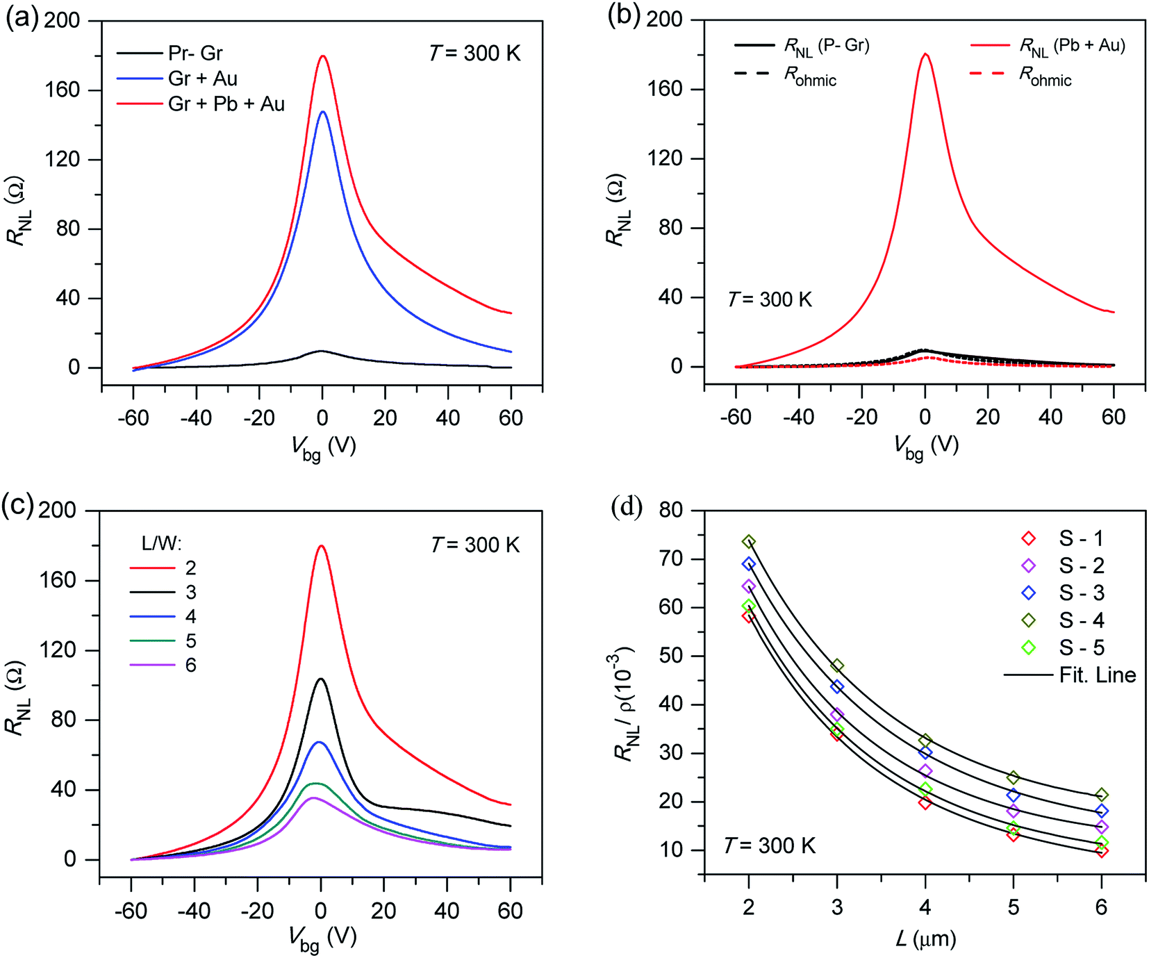 | ||
| Fig. 2 (a) Comparison of non-local signal in pristine graphene, graphene + Au, and graphene + Pb + Au. (b) Non-local resistance measurement of pristine graphene (P-Gr) and under Pb device for L/W = 2 as a function of back-gate voltages. Dotted lines are the ohmic contributions in P-Gr and under Pb + Au. (c) Non-local measurement of the device under Pb + Au (c) non-local resistance of graphene devices under Pb as a function of back-gate voltages at different L/W ratios. (d) Non-local resistance near charge neutrality points of Gr as a function of a length under Pb + Au. We measured different samples as denoted by S-1, S-2, S-3, S-4, and S-5. | ||
Thus there is no spin Hall effect (SHE) signature in pristine Gr;13,31–33 therefore, it must have an extrinsic origin. To examine this, we deposited an Au layer on the Gr and measured an NL signal up to RNL = 150 Ω. Next, we used a thin layer of Pb as an intercalated layer between the Gr and Au. Following this, we measured the Gr under the Pb and Au in the non-local configuration. We observed a very large and strong non-local signal (RNL = 180 Ω), and the contribution of ohmic leakage contribution is very small compared to pristine Gr, as shown in Fig. 2b. The value of RNL we obtained is much higher than those previously reported.13,31
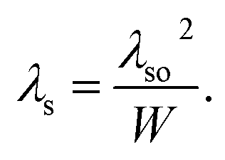
We have measured the non-local spin Hall signal of Gr/Pb/Au heterostructure by changing the thickness of Pb layer with a constant layer of Au (10 nm). We used different thickness of intercalated Pb layer (0 nm, 0.5 nm, 1 nm, and 2 nm). We confirmed the thickness of Pb and Au as shown in Fig. 4a and b. We observed that the NL signal was increased with the increasing thickness of Pb layer (Fig. 4c). For the Pb layer thicker than 1 nm, the magnitude of the NL signal saturates as shown in Fig. 4d. We attribute the large NL signal to the lattice mismatch among the graphene, Pb, and Au. It was previously reported that the intercalated Pb atoms were located in the equivalent positions to graphene A and B sublattices as compared to other heavy metal atoms. The intercalated layer of Pb significantly modified the band structure of graphene.34 Basically, the Pb atoms are more diffusive in the closer vicinity of the carbon atoms and enhance the SOI in graphene. At a larger thickness, the effect of Pb saturates due to filling of vicinity states of graphene. In addition, the Pb and Gr make a larger hybridization because the Pb layer is adjacent to the Gr sheet. The hybridization and charge carrier transfer to Gr sheet strongly affect electronic properties of graphene and SOI in graphene.35
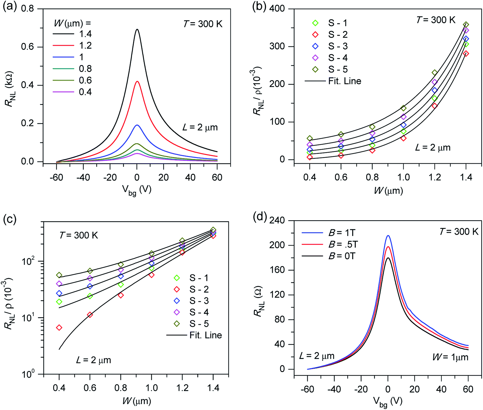 | ||
| Fig. 3 (a) Non-local resistance of graphene devices under Pb + Au as a function of back-gate voltages at different widths (W) at a fixed length at 300 K. (b) Non-local resistance near charge neutrality points of Gr as a function of width under Pb in different samples denoted as S-1 to S-5. (c) Linear dependence of Ln RNL with W that confirms that the signal comes from the SHE. We measured different samples denoted by S-1, S-2, S-3, S-4, and S-5. (d) Non-local resistance as a function of back-gate voltage at different perpendicular magnetic field room temperature with L/W = 2 μm. This increment in the RNL near the neutrality point (NP) can be assumed to be the combined effect of Zeeman splitting and bipolar transport at the charge NP under the perpendicular external magnetic field. | ||
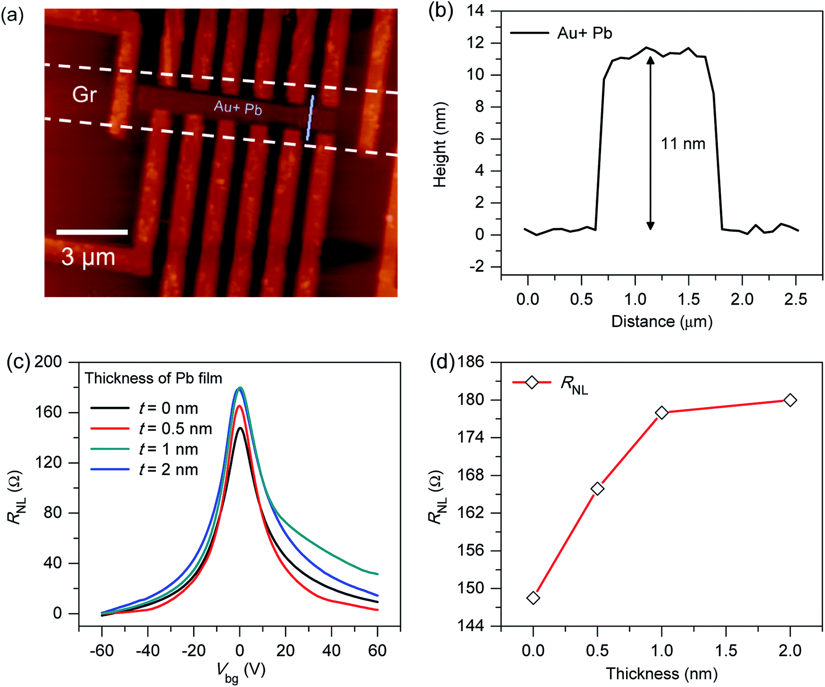 | ||
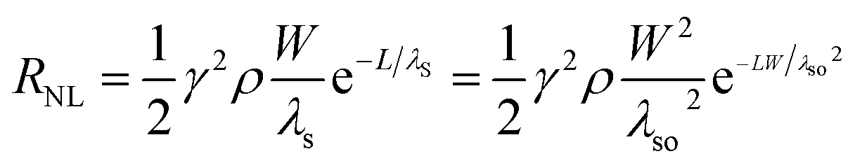
| Fig. 4 (a) Atomic force microscopy image of the final device to confirm the thickness of Au and Pb (b) height profile of Au and Pb region. Total height is 11 nm which includes 1 nm Pb and 10 nm Au. (c) Non-local signal with respect to the thickness of Pb layer. (d) Change in non-local signal with respect to thickness of the Pb film. | ||
When Pb was used as an intercalated layer between graphene and Au, the electronic structure of Gr was improved and electrons maintained a strong SOI during tunneling through Pb.34–36 Further, we estimated the NL signals as a function of the back-gate voltage at different values of L (2–5 μm) as shown in Fig. 2c. We noted that the NL signal decreased as the length of the device decreased. To determine key spin parameters such as the spin diffusion length (λs), spin relaxation time (τs), and SOI in our heterostructure device, we performed length-dependent NL signal measurements. We plotted RNL/ρ against the length of the channel and the resultant cures were fitted by the spin diffusion equation,32,37
 38 We extract λs and γ in the range of (0.20–0.62 μm) and (0.170–0.32) near the CNP, respectively.
Further, confirming the nature of the SHE, we performed width-dependent NL signal measurements. Fig. 3a shows the NL signal as a function of the back-gate voltage with a fixed channel length (L = 1 μm) and varying channel width (W = 0.4–1.4 μm). In this case, when varying the width, we only selected the devices in which the condition λs, λso > W was fulfilled. The NL signal increased as the width of channel increased. Then, we plotted RNL/ρ as a function of W near the CNP again and fitted the data by using the spin diffusion equation as shown in Fig. 3b. Thus, the estimated values of λs and γ were in the range of (0.120–0.72 μm) and (0.12–0.36) and showed good agreement with the length-dependent NL signals. Fig. 3c shows the linear dependence of ln(RNL/ρ) on W, which also confirms that the SHE shows a power-law dependence. The linear dependency of NL signals confirmed that the expected signal is caused by the SHE. If the dominant NL signal is caused owing to ohmic contribution, non-linear behaviour should be observed.31 Notably, we observed a giant and obvious NL signal as compared to ohmic contribution. Such a signal can only be observed when the width of the channel is smaller than the distance between the electrode.32,37Fig. 3d shows NL resistance as a function of the back-gate voltage (Vbg) at different perpendicular magnetic fields (B⊥) at 300 K with L/W = 2. This increment in RNL and Hall resistivity near the CNP can be attributed to the combined effect of Zeeman splitting and bipolar transport at the CNP under an external magnetic field.39,40
Moreover, to confirm the origin of the observed NL signal, we measured the current–voltage (I–V) characteristics. The linear relationship between NL voltage and the applied current excludes any possible contribution of the thermoelectric effect as shown in Fig. S2.† We can exclude such a contribution because we measured the NL voltage drop along the width of the channel and the temperature gradient due to the thermoelectric effect acts along the length of the sample. We also measured the resistance as a function of the temperature as shown in Fig. S3.† We observed a logarithmic increase in resistance with temperature at the CNP. This effect may originate from WL, disorderness due to electron–electron interaction, or the Kondo effect.41,42
We evaluated τs by τs = λs2/D, where D is the diffusion constant and can be obtained using the Einstein relation σ = e2DcN2D(EF). Here, N2D(EF) is the density of the state of Gr. Thus, the estimated value of the spin relaxation time was τs ∼ 2–4 ps. We also estimated the strength of the SOI in our device. For this estimation, we assumed that the Elliott–Yafet dephasing mechanism is dominant in our case because the spin relaxation time is directly proportional to the momentum scattering time (τs ∝ τp)31,43,44 as shown in Fig. 6a. We calculated the SOI using the following relation, 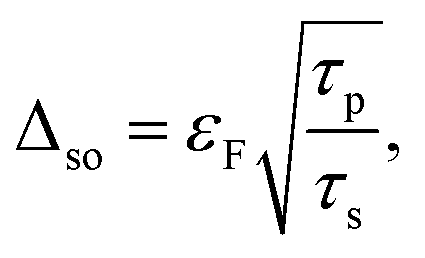 where εF is the Fermi energy and τp is the momentum scattering time
  and vF is the Fermi velocity. The obtained value of SOI is 70–90 meV, which is greater than previously reported values in hydrogenated graphene (≈2.5 meV) and fluorinated graphene (≈5.1 meV).12,13 Thus, the presence and enhancement in the NL signal at room temperature and zero magnetic field (B = 0 T) enhances the SOI in Gr.2,30,45 The spin current in Gr via the SHE and the inverse SHE could be detected as the SOI was enhanced.
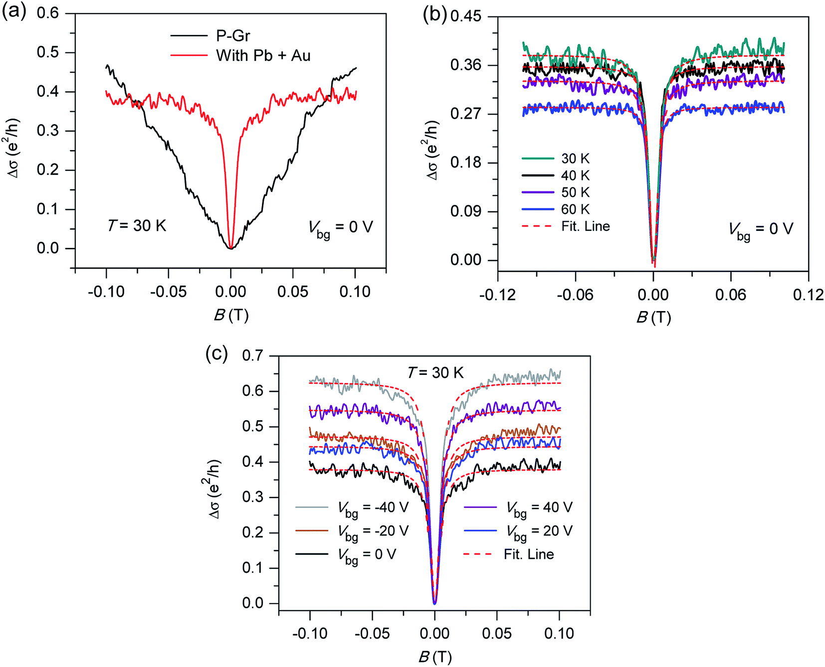 | ||
| Fig. 5 (a) Magnetoconductance (MC) curves measured before and after the deposition of Pb + Au at 30 K (b) weak localization curves at various temperatures; the red line is the fitting line. (c) Back gate-dependent weak localization curves at 30 K. | ||
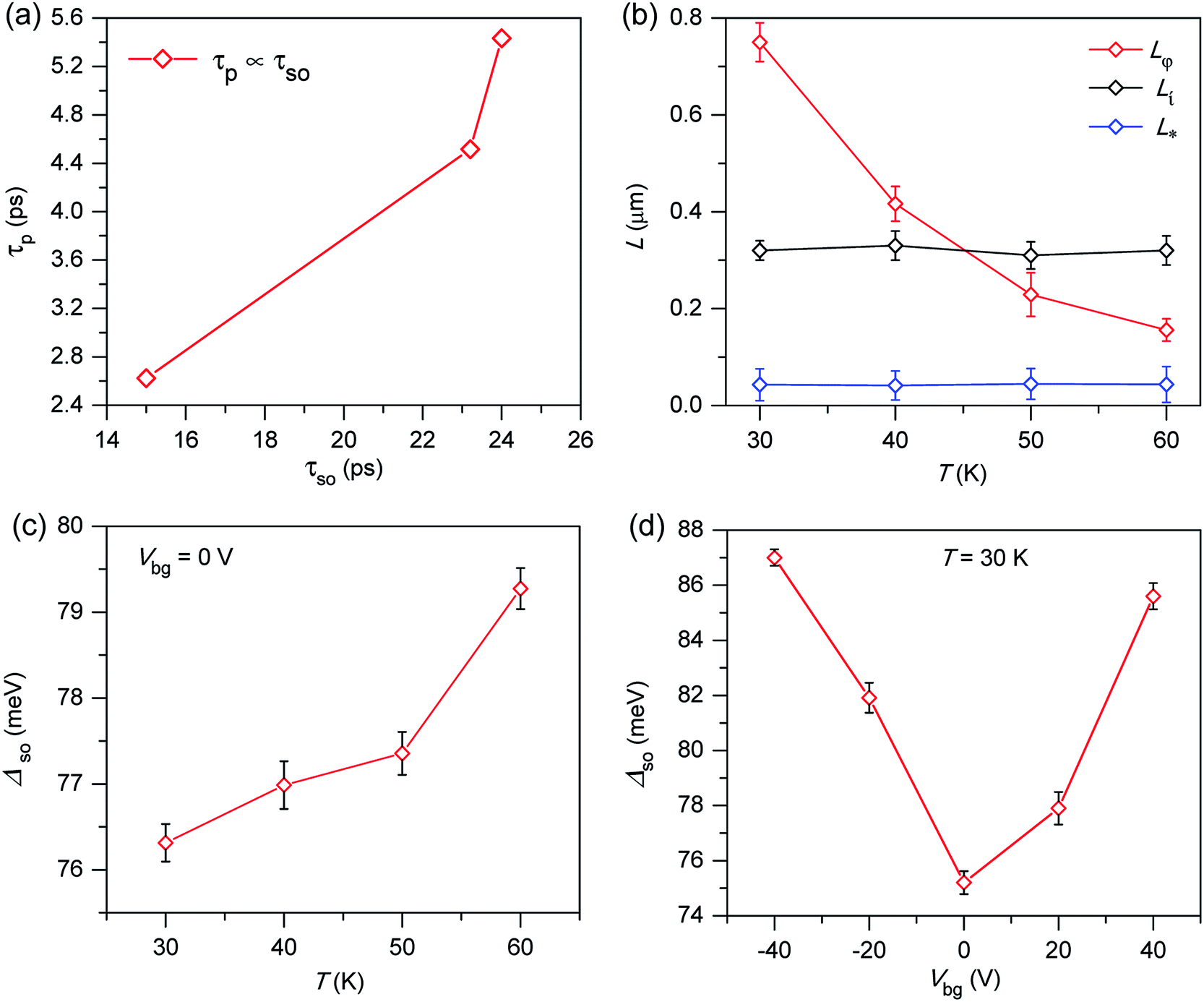 | ||
| Fig. 6 (a) Relation between spin relaxation time and momentum scattering time (b) temperature-dependent dephasing length Lφ with error bars derived from WL formula fitting. (c) Temperature-dependent spin-orbital interaction of graphene under Pb and Au that linearly increases with temperature. (d) Gate-dependent SOI in graphene under Pb and Au. | ||
We further estimated the strength of the SOI in the Gr sheet by analyzing the WL signal near the zero field.46,47 The WL signal was dominant near B = 0 T as compared to pristine Gr as shown in Fig. 5a. We could observe the WL signals only at low temperatures as shown in Fig. 5b. We also measured the gate dependent magnetoconductance at 30 K, as shown in Fig. 5c. The suppression of the WL signal agreed with the Kane–Mele SOI in our measurement. Thus, we used the following equation to fit the WL data,46

 D is the charge carrier diffusion constant, and τφ−1 is the dephasing rate. τi−1 describes the inter-valley scattering time, τ*−1 is the intra-valley scattering time, and τso−1 is the intrinsic KM spin relaxation time. Using the temperature-dependent WL data, we extracted the dephasing rate as shown in Fig. 6b. The dephasing length decreased as the temperature increased from 30 to 60 K, which can be attributed to electron–electron interaction. Moreover, τso can be related to the strength of the SOI by
 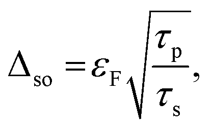 where εF is the Fermi energy. The estimated value of the SOI is 50–60 meV. The temperature- and gate-dependent SOIs are shown in Fig. 6c and d. The SOI was observed to vary with temperature; this change may be owing to the contribution of temperature-dependent scattering, ionic centers, and phonons.
In summary, we fabricated Gr FET, in which Pb was used as the intercalated layer between Gr and Au. We measured the electronic properties in pristine Gr and Gr with Pb + Au; their mobilities were 25000 cm2 V−1 s−1 and 29100 cm2 V−1 s−1, respectively. The mobility increased by the intercalation of Pb because it modified the electronic structure of Gr. To confirm the SHE, we performed length- and width-dependent NL signal measurements in pristine Gr and with adatoms. We observed a giant NL signals of 150 Ω and 180 Ω with only Au and with Pb + Au, respectively. Further, we calculated key parameters such as spin λs, τs, and γ in the range of (0.20–0.62 μm), (0.40–0.62 ps), and (0.170–0.32), respectively, near the CNP. The strength of the SOI was 80–90 meV. Moreover, we performed the WL measurements to confirm the self-consistency. The SOI strength was close to the calculated value according to the NL signal measurements. The thin metal films on Gr lead to an enhanced SOI and a SHE with a large spin Hall coefficient. The SHE and SOI were enhanced by the proximity-induced effect due to adatoms of heavy metals.34,45 In particular, the observed SHE stems from extrinsic origins such as skew scattering and quantum-side jumps.
Device fabrication
A Gr flake from commercial graphite was exfoliated micro-mechanically on SiO2/highly p-doped Si (300 nm) substrate by using the standard Scotch tape method. A monolayer Gr can be identified with appropriate thickness due to the interference effect. Further, Raman spectroscopy was used to confirm the thickness of Gr. After making the large pattern, the samples were annealed at 400 °C for 6 h under Ar/H2 (97.5% Ar/2.5% H2) gas flow. Electron-beam lithography (EBL) and O2 plasma were used to design the electrodes in the Hall bar (H) configuration, and Cr/Au (6/60 nm) was deposited by thermal evaporation. Moreover, we made a small window with EBL and deposited Pb and Au (1 nm/10 nm) thin films through thermal evaporation. The length and width of the Gr channel were 1–6 μm and 0.4–1.4 μm, respectively.The Raman spectra of Gr were measured with a Renishaw micro-spectrometer over a wavenumber range of 1100–3200 cm−1, with a laser wavelength of 514.5 nm. To prevent the device from experiencing local heating, the spot size was fixed as 1 μm, and the power was maintained at 1.0 mW. To examine the surface morphology of Gr, an atomic force microscope (AFM) was used. The local and non-local measurements of the Gr/Pb/Au heterostructure device were performed by using the standard lock-in technique at different temperatures with or without a magnetic field.
Conflicts of interest
There are no conflicts to declare.Acknowledgements
This work was supported by the Basic Science Research Program (2016R1D1A1A09917762, 2019R1F1A1057697) and the Global Research and Development Center Program (2018K1A4A3A01064272) through the National Research Foundation of Korea (NRF) grant funded by the Korea government (Ministry of Education and the Ministry of Science and ICT).References
- S. A. Wolf, D. D. Awschalom, R. A. Buhrman, J. M. Daughton, S. von Molnár, M. L. Roukes, A. Y. Chtchelkanova and D. M. Treger, Science, 2001, 294, 1488–1495 CrossRef CAS.
- K. S. Novoselov, A. K. Geim, S. V. Morozov, D. Jiang, Y. Zhang, S. V. Dubonos, I. V. Grigorieva and A. A. Firsov, Science, 2004, 306, 666–669 CrossRef CAS.
- A. K. Geim and K. S. Novoselov, in Nanoscience and Technology: A Collection of Reviews from Nature Journals, World Scientific, 2010, pp. 11–19 Search PubMed.
- N. Tombros, C. Jozsa, M. Popinciuc, H. T. Jonkman and B. J. Van Wees, Nature, 2007, 448, 571 CrossRef CAS.
- M. V. Kamalakar, C. Groenveld, A. Dankert and S. P. Dash, Nat. Commun., 2015, 6, 6766 CrossRef CAS.
- W. Han, R. K. Kawakami, M. Gmitra and J. Fabian, Nat. Nanotechnol., 2014, 9, 794 CrossRef CAS.
- S. Datta and B. Das, Appl. Phys. Lett., 1990, 56, 665–667 CrossRef CAS.
- A. H. Castro Neto and F. Guinea, Phys. Rev. Lett., 2009, 103, 026804 CrossRef CAS.
- F. Schedin, A. K. Geim, S. V. Morozov, E. W. Hill, P. Blake, M. I. Katsnelson and K. S. Novoselov, Nat. Mater., 2007, 6, 652 CrossRef CAS.
- F. Kuemmeth, S. Ilani, D. Ralph and P. McEuen, Nature, 2008, 452, 448 CrossRef CAS.
- D. Huertas-Hernando, F. Guinea and A. Brataas, Phys. Rev. B: Condens. Matter Mater. Phys., 2006, 74, 155426 CrossRef.
- J. Balakrishnan, G. K. W. Koon, M. Jaiswal, A. C. Neto and B. Özyilmaz, Nat. Phys., 2013, 9, 284 Search PubMed.
- A. Avsar, J. H. Lee, G. K. W. Koon and B. Özyilmaz, 2D Materials, 2015, 2, 044009 Search PubMed.
- H. Zhang, C. Lazo, S. Blügel, S. Heinze and Y. Mokrousov, Phys. Rev. Lett., 2012, 108, 056802 CrossRef.
- C. Weeks, J. Hu, J. Alicea, M. Franz and R. Wu, Phys. Rev. X, 2011, 1, 021001 Search PubMed.
- M. J. Piotrowski, P. Piquini and J. L. Da Silva, Phys. Rev. B: Condens. Matter Mater. Phys., 2010, 81, 155446 CrossRef.
- S. Blügel, Phys. Rev. Lett., 1992, 68, 851–854 CrossRef.
- S. V. Morozov, K. S. Novoselov, M. I. Katsnelson, F. Schedin, L. A. Ponomarenko, D. Jiang and A. K. Geim, Phys. Rev. Lett., 2006, 97, 016801 CrossRef CAS.
- H. Haugen, D. Huertas-Hernando and A. Brataas, Phys. Rev. B: Condens. Matter Mater. Phys., 2008, 77, 115406 CrossRef.
- P. Wei, S. Lee, F. Lemaitre, L. Pinel, D. Cutaia, W. Cha, F. Katmis, Y. Zhu, D. Heiman and J. Hone, Nat. Mater., 2016, 15, 711 CrossRef CAS.
- Z. Wang, C. Tang, R. Sachs, Y. Barlas and J. Shi, Phys. Rev. Lett., 2015, 114, 016603 CrossRef.
- Z. Wang, D. K. Ki, H. Chen, H. Berger, A. H. MacDonald and A. F. Morpurgo, Nat. Commun., 2015, 6, 8339 CrossRef CAS PubMed.
- A. Avsar, J. Y. Tan, T. Taychatanapat, J. Balakrishnan, G. K. W. Koon, Y. Yeo, J. Lahiri, A. Carvalho, A. S. Rodin, E. C. T. O'Farrell, G. Eda, A. H. Castro Neto and B. Özyilmaz, Nat. Commun., 2014, 5, 4875 CrossRef CAS.
- A. M. Afzal, M. F. Khan, G. Nazir, G. Dastgeer, S. Aftab, I. Akhtar, Y. Seo and J. Eom, Sci. Rep., 2018, 8, 3412 CrossRef.
- A. C. Ferrari, J. C. Meyer, V. Scardaci, C. Casiraghi, M. Lazzeri, F. Mauri, S. Piscanec, D. Jiang, K. S. Novoselov, S. Roth and A. K. Geim, Phys. Rev. Lett., 2006, 97, 187401 CrossRef CAS.
- D. Graf, F. Molitor, K. Ensslin, C. Stampfer, A. Jungen, C. Hierold and L. Wirtz, Nano Lett., 2007, 7, 238–242 CrossRef CAS PubMed.
- J. Y. Tan, A. Avsar, J. Balakrishnan, G. K. W. Koon, T. Taychatanapat, E. C. T. O'Farrell, K. Watanabe, T. Taniguchi, G. Eda, A. H. C. Neto and B. Özyilmaz, Appl. Phys. Lett., 2014, 104, 183504 CrossRef.
- Z. Wang, D.-K. Ki, J. Y. Khoo, D. Mauro, H. Berger, L. S. Levitov and A. F. Morpurgo, Phys. Rev. X, 2016, 6, 041020 Search PubMed.
- F. V. Tikhonenko, D. W. Horsell, R. V. Gorbachev and A. K. Savchenko, Phys. Rev. Lett., 2008, 100, 056802 CrossRef CAS PubMed.
- K. Kim, S. Larentis, B. Fallahazad, K. Lee, J. Xue, D. C. Dillen, C. M. Corbet and E. Tutuc, ACS Nano, 2015, 9, 4527–4532 CrossRef CAS.
- J. Balakrishnan, G. Kok Wai Koon, M. Jaiswal, A. H. Castro Neto and B. Özyilmaz, Nat. Phys., 2013, 9, 284 Search PubMed.
- D. Abanin, A. Shytov, L. Levitov and B. Halperin, Phys. Rev. B: Condens. Matter Mater. Phys., 2009, 79, 035304 CrossRef.
- G. Mihajlović, J. Pearson, M. Garcia, S. Bader and A. Hoffmann, Phys. Rev. Lett., 2009, 103, 166601 CrossRef.
- F. Calleja, H. Ochoa, M. Garnica, S. Barja, J. J. Navarro, A. Black, M. M. Otrokov, E. V. Chulkov, A. Arnau and A. L. V. De Parga, Nat. Phys., 2015, 11, 43 Search PubMed.
- I. I. Klimovskikh, M. M. Otrokov, V. Y. Voroshnin, D. Sostina, L. Petaccia, G. Di Santo, S. Thakur, E. V. Chulkov and A. M. Shikin, ACS Nano, 2017, 11, 368–374 CrossRef CAS.
- D. Ma and Z. Yang, New J. Phys., 2011, 13, 123018 CrossRef.
- S. Kettemann, Phys. Rev. Lett., 2007, 98, 176808 CrossRef.
- J. Balakrishnan, G. K. W. Koon, A. Avsar, Y. Ho, J. H. Lee, M. Jaiswal, S.-J. Baeck, J.-H. Ahn, A. Ferreira and M. A. Cazalilla, Nat. Commun., 2014, 5, 4748 CrossRef CAS.
- D. Abanin, R. Gorbachev, K. Novoselov, A. Geim and L. Levitov, Phys. Rev. Lett., 2011, 107, 096601 CrossRef CAS.
- D. Abanin, S. Morozov, L. Ponomarenko, R. Gorbachev, A. Mayorov, M. Katsnelson, K. Watanabe, T. Taniguchi, K. Novoselov and L. Levitov, Science, 2011, 332, 328–330 CrossRef CAS.
- S. Lara-Avila, A. Tzalenchuk, S. Kubatkin, R. Yakimova, T. Janssen, K. Cedergren, T. Bergsten and V. Fal’ko, Phys. Rev. Lett., 2011, 107, 166602 CrossRef.
- J.-H. Chen, L. Li, W. G. Cullen, E. D. Williams and M. S. Fuhrer, Nat. Phys., 2011, 7, 535 Search PubMed.
- H. Ochoa, A. C. Neto and F. Guinea, Phys. Rev. Lett., 2012, 108, 206808 CrossRef CAS.
- D. Huertas-Hernando, F. Guinea and A. Brataas, Phys. Rev. Lett., 2009, 103, 146801 CrossRef CAS.
- J. Balakrishnan, G. K. W. Koon, A. Avsar, Y. Ho, J. H. Lee, M. Jaiswal, S.-J. Baeck, J.-H. Ahn, A. Ferreira, M. A. Cazalilla, A. H. C. Neto and B. Özyilmaz, Nat. Commun., 2014, 5, 4748 CrossRef CAS.
- E. McCann and V. I. Fal’ko, Phys. Rev. Lett., 2012, 108, 166606 CrossRef.
- E. McCann and M. Koshino, Phys. Rev. B: Condens. Matter Mater. Phys., 2010, 81, 241409 CrossRef.
Footnote |
| † Electronic supplementary information (ESI) available. See DOI: 10.1039/c9ra06961e |
| This journal is © The Royal Society of Chemistry 2019 |