DOI:
10.1039/C9RA06873B
(Paper)
RSC Adv., 2019,
9, 36113-36122
Effect of Fe ion implantation on the thermoelectric properties and electronic structures of CoSb3 thin films
Received
29th August 2019
, Accepted 14th October 2019
First published on 6th November 2019
Abstract
In the present study, thin films of single-phase CoSb3 were deposited onto Si(100) substrates via pulsed laser deposition (PLD) method using a polycrystalline target of CoSb3. These films were implanted by 120 keV Fe-ions with three different fluences: 1 × 10¹⁵, 2.5 × 10¹⁵ and 5 × 10¹⁵ ions per cm2. All films were characterised by X-ray diffraction (XRD), Raman spectroscopy, atomic force microscopy (AFM), Rutherford backscattering (RBS) spectrometry and X-ray absorption spectroscopy (XAS). XRD data revealed that the ion implantation decreased the crystalline nature of these films, which are recovered after the rapid thermal annealing process. The Seebeck coefficient S vary with the fluences in the temperature range of 300 K to 420 K, and is found to be highest (i.e., 254 μV K−1) at 420 K for the film implanted with 1 × 10¹⁵ ions per cm2. The high S and low resistivity lead to the highest power factor for the film implanted with 1 × 10¹⁵ ions per cm2 (i.e., 700 μW m−1 K−2) at 420 K. The changing of the sign of S from negative for the pristine film to positive for the Fe-implanted samples confirm that the Fe ions are electrically active and act as electron acceptors by replacing the Co atoms. XAS measurements confirm that the Fe ions occupied the Co site in the cubic frame of the skutterudite and exist in the 3+ oxidation state in this structure.
1. Introduction
Skutterudites have gained considerable attention in the field of thermoelectrics because of their open structure and their applications, such as in the harvesting of waste heat generated in industries and thermoelectric refrigeration.1 An efficient thermoelectric material must have low electrical resistivity (ρ), low thermal conductivity (κ) and a high Seebeck coefficient (S) related by a dimensionless quantity known as the figure of merit, zT = S2T/ρκ, where κ is the lattice thermal conductivity that is the sum of κel (heat conducted by carriers) and κlat (from the lattice).2 The enhancement in zT can be done either by increasing the power factor S2/ρ or by decreasing κ. CoSb3 is a low band gap skutterudite compound semiconductor with high S and high carrier mobility.3 It has a cubic structure with the formula of MX3, where M is a metal ion, such as Co, Rh, and Ir, and X is any metalloid (such as As and Sb). Of the eight sub-cubes in a cubic unit cell, two cubes are voids that can accommodate guest atoms and rattle inside.2 Among different skutterudites, CoSb3 shows the best thermoelectric properties as it owns excellent electronic properties,1,4,5 although its use in practical applications is limited due to its high lattice thermal conductivity.6 However, κ can be decreased by filling the voids with rattler atoms,7 by nanostructuring8,9 or by ion implantation.10 Ion implantation is one of the novel ways for modifying the electronic and thermoelectric properties of materials.11,12 During ion implantation, doping can be done in a controlled way that enhances the electrical conductivity by increasing the carrier concentration. Simultaneously, it can affect the lattice thermal conductivity by creating lattice defects and disorders. By ion implantation, the void can be filled or occupy the Co or Sb sites that act as electron donors or acceptors, leading to p- and n-type semiconductors.11,12 These dopants can also act as phonon scattering centres and help in reducing the lattice thermal conductivity. Ion implantations by Fe,13–15 Ni16 or light ions (such as B or C ions) are expected to occupy the Co or Sb sites, whereas metals such as Th, Ur, La,6,7 Eu17 or Ce18,19 ions are expected to occupy voids and rattle inside. Such rattling is expected to dramatically reduce the lattice thermal conductivity. Nolas et al.20 studied the thermoelectric properties on bulk Yb-filled skutterudite and found zT to be close to 1 at 600 K for Yb0.19Co4Sb12. Wang et al.21 reported a high zT of 1.5 at 850 K for Yb0.3Co4Sb12, which is the highest filled value for single filled Co4Sb12. Shi et al.22 investigated multi-filled skutterudite bulk materials and was able to achieve a high zT of 1.7 at 850 K. Doping with Fe creates three holes per defect, which reduces the thermal conductivity and also changes the electronic properties of CoSb3.23 Katsuyama et al. found that the presence of a second phase in the Co–Fe–Sb ternary system enhanced the figure of merit by suppressing the electrical resistivity and thermal conductivity.24 Kim et al. showed that Co0.7Fe0.3Sb3 samples have a thermal conductivity value at around 0.03 W m−1 K−1 and S value of 114 μV K−1 at 700 K.25 For the skutterudites to be used in device applications, it is necessary to find such promising “bulk” properties in the thin films of skutterudite. Savchuk et al.26 studied the structural and transport properties of the n-type polycrystalline CoSb3 thin films grown on oxidised Si(100) and on Al2O3 substrates by dc magnetron sputtering and obtained a S value of −250 μV K−1 at ∼550 K for both substrates and a thermal conductivity of 3 W (mK)−1 at room temperature. Daniel et al.27 studied the thermoelectrical properties of CoSb3 thin films deposited by molecular beam deposition at different substrate temperatures, and showed that the films exhibited bipolar conduction behaviour indicated by a positive Hall constant and a negative S. Kumar et al.28 studied the thermoelectric properties of In and Yb-doped polycrystalline thin films prepared by PLD and obtained the highest power factor of 0.68 W (mK)−1 at ∼700 K. In yet another study,29 they reported on the lattice dynamics and thermoelectric properties of the above compounds on different substrates at an elevated temperature, and found that the In and Yb dopants occupy the cage sites in the skutterudite lattice. Suchitra et al.30 studied the incorporation of MoS2 nanosheets in a CoSb3 matrix and reported a zT of 0.53 at 600 K for the CoSb3/MoS2 nanocomposite containing 3 wt% of MoS2, which is 4 times higher than that for the pristine sample. Recent studies by Bala et al.11 found an enhancement in the thermoelectric power due to Ni ion implantation. However, there is no literature found on the studies of doping of Fe on CoSb3 by the ion implantation method. Among the thin film deposition techniques that have been carried out for the deposition of pure phase CoSb3 are the solvothermal,31 RF sputtering,32,33 pulsed laser deposition (PLD)34–37 and DC sputtering.26 Of these techniques, PLD has proven to be one of the well-suited methods for the deposition of CoSb3 films with proper stoichiometry.
The present study focuses on the morphological, structural, electrical and thermoelectric properties of the Fe ion-implanted CoSb3 thin films deposited by PLD. Further, X-ray absorption spectroscopy has been used to understand the local electronic structures of these Fe-implanted CoSb3 samples.
2. Experimental details
The bulk CoSb3 target was prepared by the solid-state reaction method. High purity Co and Sb powders (Alfa-Aesar, 99.98%) were mixed in a stoichiometric ratio to make a 1 inch target. The mixed powders were sealed in an evacuated quartz tube (<10−4 torr) and placed in a programmable furnace. The temperature was increased to 1323 K in 6 h, and then held for 24 h. It was then allowed to cool to 923 K in 48 h. It was held at the same temperature for 72 h, and then allowed to cool naturally to room temperature. The polycrystalline material was ground for 3 h and then pelletised with a 1 inch diameter pellet. It was annealed several times under an Ar gas environment. The target was brittle and had a dark grey metallic lustre. The structure and composition of the target was determined by powder X-ray diffraction (XRD). The films were deposited onto Si(100) substrates using the PLD system from M/S Excel Instruments, Mumbai. The PLD growth chamber was evacuated to a base pressure of 1.5 × 10⁻⁷ torr. The deposition was done in the presence of Ar gas with a working pressure of 1.3 × 10⁻² mbar. The presence of Ar gas during deposition is expected to provide a better thermalisation of the species in the ablation plume.17 During the deposition, the target was continuously rotated for the uniform ablation of the target surface to obtain uniformity in the deposited films. The target-to-substrate distance was kept fixed at 6 cm. The substrates were maintained at a temperature of 523 K during deposition. The substrates were held onto the substrate holder by Ag paste. Reports suggested that the use of Ag paste in sticking the substrates helps in reducing the isotropic compressive stress that causes blistering of the CoSb3 films.37 The cumulative effects of the large target-substrate distance, the presence of Ar gas, and the use of Ag paste ensured that all the grown films were free of blistering. A KrF excimer laser (248 nm) (Coherent Inc.) with a pulse duration of 20 ns and fixed repetition rate of 10 Hz was used for ablation. A laser fluence of 184 mJ per pulse (corresponding to an energy density of 4.6 J cm−2) was used. After optimisation, the number of shots was fixed to 7272 (250 nm). It should be noted that the above-mentioned thickness is only the nominal thickness using surface profilometry. The deposited films were then implanted with 120 keV Fe ions using the Negative Ion Implanter facility of IUAC New Delhi with three different fluences: 1 × 10¹⁵, 2.5 × 10¹⁵ and 5 × 10¹⁵ ions per cm2. The implantation was carried out at room temperature with the vacuum maintained at 10−6 torr. All films were then annealed using the rapid thermal annealing (RTA) technique. The RTA was done for 2 min at 873 K under Ar gas. For convenience hereafter, the pristine film will be referred to as P; the rapid annealed film as PA; the films 1 × 10¹⁵, 2.5 × 10¹⁵ and 5 × 10¹⁵ as I1E15, I2.5E15 and I5E15, respectively; and the implanted (but rapid-annealed) samples as I1E15A, I2.5E15A and I5E15A. The structural characterizations were performed using grazing incidence X-ray diffraction (GIXRD) at 1° with the Philips X'pert PRO (Model PW 3040) diffractometer. The micro Raman measurements were conducted using a Micro Raman spectroscopy system (m-RS, Renishaw, UK). The reflectance was examined by a UV-vis NIR spectrophotometer (Shimadzu-3101PC, Japan) using unpolarized light. Rutherford backscattering (RBS) spectrometry was performed using the 1.7 MV tandem accelerator facility with 2 MeV He+ ions at a scattering angle of 165° at IUAC, New Delhi for compositional and depth profile studies. The data were analysed using the Rutherford Universal Simulation Program (RUMP). AFM was employed to study the surface morphology using the MultiMode® scanning probe microscope (Bruker) in tapping mode. The electrical resistivity (ρ) and the Seebeck coefficient (S) were measured by the four-probe method and the bridge method,38 respectively, in the temperature range from 300 K to 400 K. The soft X-ray absorption spectroscopy (XAS) measurements at the Co L- and Fe L-edges were performed at the BL20A1 HSGM beamline, Sb L3-edge was performed at the 16A1 Tender X-ray absorption beamline, and the Fe K edge was performed at the 17C1 beamline of the National Synchrotron Radiation Research Centre (NSRRC) in Taiwan. The spectra at the Fe and Co L2,3-edges were recorded in the total electron yield (TEY) mode, while the Sb L3- and Fe K-edges were recorded in the total fluorescent yield (TFY) mode with a photon energy resolution of 0.3 eV.
3. Results and discussion
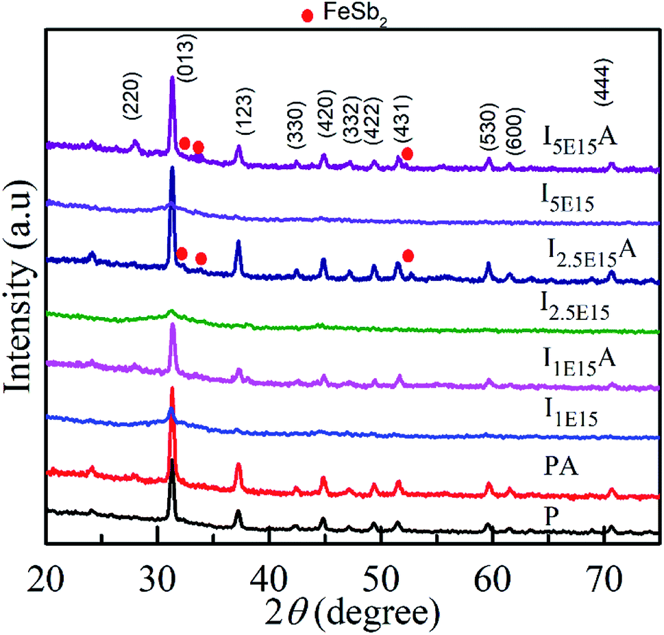
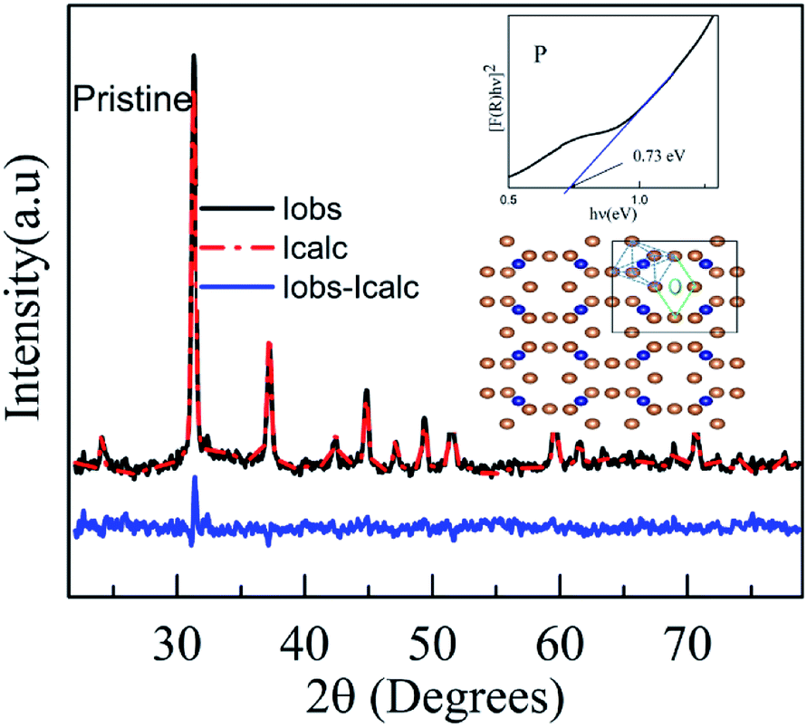
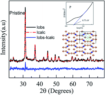
The structure and phase of the PLD-deposited films were determined by GIXRD. Fig. 1 shows the GIXRD pattern of P, PA, I1E15, I1E15A, I2.5E15, I2.5E15A, I5E15, and I5E15A. The pristine as-deposited films were polycrystalline and single phase in nature, and the indexing of the peaks were done based on the simple cubic structure of CoSb3 (JCPDS 19-0336). Due to ion implantation, the films became amorphized and regained their crystallinity after the RTA process under Ar atmosphere. In order to obtain electrically active doped regions, the implanted material needs to be annealed to restore the crystal lattice and relocate the implanted atoms onto substitutional sites where they can become electrically active. During the regrowth of the amorphous layers in CoSb3, the implanted dopant can take up substitutional lattice positions or accommodate in void spaces depending on the dopant concentration and size of the dopant atom. Due to the high Sn (nuclear energy loss, 106 eV nm−1) during implantation, extended damages lead to the creation of vacancies through nuclear collisions. The vacancies created as calculated by the TRIM39 (transport of ions in matter) software are 2213.8 per Fe ion. The projected range is 60 nm with a straggling of 30 nm. Based on this, it was found that a ∼90 nm thick layer is amorphized. The remaining crystalline layer enables the recrystallisation of films after the RTA process. There were no traces of secondary phases of Co or Sb ions within the detection limit of the samples (JCPDS 03-0717). This FeSb2 impurity has been reported earlier at higher doping concentrations.24 Fig. 2 shows the Rietveld refined pattern of the pristine sample. All samples crystallized in the body centred cubic space group Im![[3 with combining macron]](https://www.rsc.org/images/entities/char_0033_0304.gif) (#204). As obtained after refinement, the unit cell volume was 73.87 nm3. The Co metal ions are located at the 8c sites (1/4, 1/4, 1/4), while the pnictogen atom Sb occupied the 24g sites (0, y, z). All the diffraction peaks match well with the reference structure, indicating the phase purity of the pristine sample. After refinement, the lattice parameter is 9.04 Å for the pristine sample. This value is in close agreement with the reported value of 9.0385 Å (JCPDS 19-0336).
(#204). As obtained after refinement, the unit cell volume was 73.87 nm3. The Co metal ions are located at the 8c sites (1/4, 1/4, 1/4), while the pnictogen atom Sb occupied the 24g sites (0, y, z). All the diffraction peaks match well with the reference structure, indicating the phase purity of the pristine sample. After refinement, the lattice parameter is 9.04 Å for the pristine sample. This value is in close agreement with the reported value of 9.0385 Å (JCPDS 19-0336).
 |
| | Fig. 1 XRD pattern of the CoSb3 thin films: P, PA, I1E15, I1E15A, I2.5E15, I2.5E15A, I5E15, and I5E15A. Note that after RTA, recrystallization is evident. | |
 |
| | Fig. 2 Rietveld refined pattern of the pristine sample. The inset (right side) shows the Tauc plot of the pristine CoSb3 sample. The structure with blue dashed lines forms the CoSb6 octahedron and the one with green dashed lines depicts the void. The brown-coloured atoms represent Sb, the blue ones are Co and the grey-coloured atom shows the guest atom. | |
Christensen et al.40 also reported a decrease in the lattice parameter after Fe doping. However, they did not observe a clear trend in the lattice parameter values. The lattice parameter and atomic coordinates obtained from these refinements were used as inputs in the Vesta41 program to visualise the crystal structure of the pristine sample. Fig. 2 shows the crystal structure of CoSb3. In this structure, the blue dashed lines show the CoSb6 octahedron and the region by the green dashed lines forms the void. The bonding between the atoms is mainly covalent in nature. The distance between the two metal atoms (Co–Co) is large so these ions do not create a bonding; hence, the bonding occurs between Sb–Sb (pnictogen atoms), creating the Sb4 rings and pnictogen and metal atom bonding (Co–Sb). The bond lengths, as obtained from the Rietveld refinement data, are Co–Sb (2.531 Å), Sb–Sb short pair (2.855 Å) and Sb–Sb long pair (3.43 Å). It is comparable with the values given in the literature for unfilled CoSb3.42 CoSb3, a narrow band-gap semiconductor, has an energy gap that lies in the far-infrared region. However, the optical characterization in the present work is limited to the UV-visible region. The optical properties of the CoSb3 thin film was analysed by UV-visible reflectance spectra. The band gap was estimated using the Kubelka–Munk (KM) equation and it was found to be 0.73 eV.32 Anno et al. have reported a band gap energy of 0.9 eV.32 However, it was found that the optical band gap varied from 0.5 to 0.9 eV.33
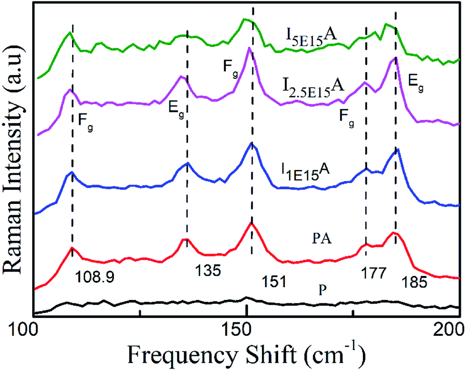
The Raman spectra of P, PA, I1E15A, I2.5E15A and I5E15A thin films measured at 300 K are shown in Fig. 3. The as-deposited P film did not show any characteristic Raman modes of CoSb3. However, after RTA, five out of eight Raman active modes are observed in all implanted and annealed samples. All these modes were assigned on the basis of group theory and the CoSb3 crystallite reported by Nolas et al.20 These peaks show a small shift when compared with that reported in the literature (Table 1).19
 |
| | Fig. 3 Raman spectra of the CoSb3 thin films: P, PA, I1E15A, I2.5E15A, and I5E15A. At the highest ion fluence, broadening is observed. | |
Table 1 Peak positions of Raman active modes of the CoSb3 films from the present work are compared with theory.19
Present work ![[small upsilon, Greek, macron]](https://www.rsc.org/images/entities/i_char_e0d5.gif) (cm−1) (cm−1) |
CoSb3 crystallite (cm−1) |
CoSb3 theory (cm−1) |
Modes assigned |
| 108.9 |
110 |
97 |
(Fg) |
| 135 |
135 |
139 |
(Eg) |
| 151 |
152 |
150 |
(Fg) |
| 178 |
179 |
179 |
(Fg) |
| 184 |
187 |
182 |
(Eg) |
The Raman active modes in the CoSb3 structure did not include any motion of the Co metal sub-lattice atoms; rather, these show the relative motion of the Sb atom with respect to each other so that the centre of mass of Sb in the unit cell does not change. The matching of the phonon frequency of all the implanted films with the literature further confirms the formation of the skutterudite structure. This implies that the Fe ions are implanted at the Co sites and not in the Sb sites. There is a small broadening observed in all implanted samples. The broadening of the peaks may be due to phonon–phonon interactions. Another possible mechanism for such broadening is the disorder caused by the random placement of Fe ions during ion implantation.
If some of the Fe ions are trapped in the voids created by the Sb atoms, they might rattle inside these voids. This rattling of the Fe ions gives rise to the fluctuating bonding of the Sb bonds that makes the boundary of the voids. This might lead to a slight broadening of the vibrational energies of the Sb rings.43 The spectral assignment has been done by comparing the vibrational energies from the literature.43 The Eg peaks at 135 cm−1 (theoretically predicted at 139 cm−1) and 184 cm−1 depict the elongation of all sides of one rectangle, while shortening of all sides of another one.43 The Fg peak at 151 cm−1 (predicted at 157 cm−1) depicts the rotation of the rectangle about an axis parallel to one side. The Fg weak peak at 176 cm−1, which is theoretically predicted at 178 cm−1, depicts the out of plane shear motion of two atoms of a rectangle along a diagonal. All peaks are in good agreement with the theoretical calculations.44
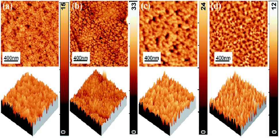
Fig. 4 shows the 2D and 3D AFM images of P, I1E15A, I2.5E15A, and I5E15A films. The suitable parameter used to characterise the surface morphology of the thin film is the root mean square (RMS) roughness. From the AFM micrograph, a change in the surface morphology by varying the Fe ion fluence is evident. The RMS surface roughness of P was 1.68 nm, which increased with ion fluences and reached up to 3.70 nm for I2.5E15A. This increase in the ion fluencies is due to the defects and disorders created by the ion beam during implantation. For I5E15A, the roughness decreased to 1.78 nm. It might be because the disorders or defects were annealed out due to local annealing at higher fluence during implantation. The grains of P were found to be uniform with an average grain size of 72.40 nm, and it increased to 95.56 nm for I1E15A. For the I2.5E15A and I5E15A samples, the grains were found to be agglomerated.
 |
| | Fig. 4 2D and 3D AFM images of (a) P, (b) I1E15A, (c) I2.5E15A, (d) I5E15A films. | |
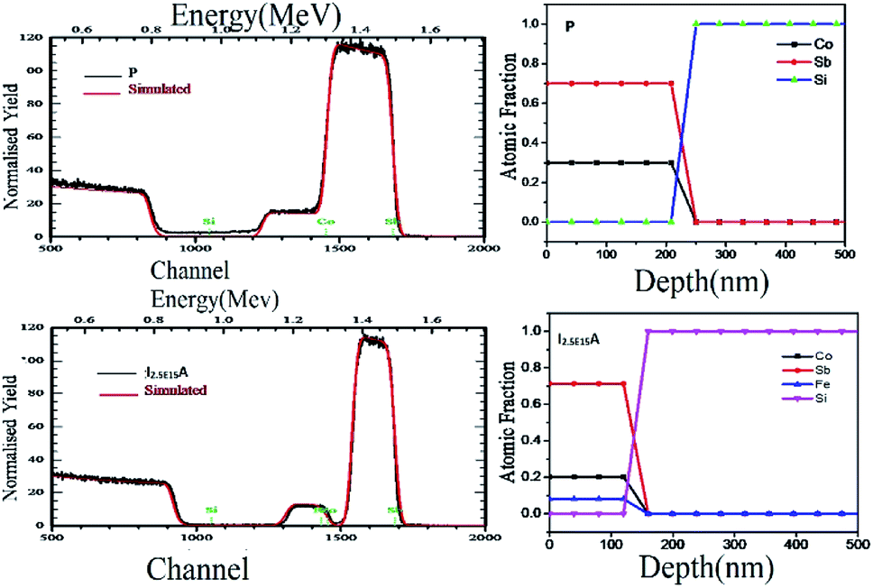
The RBS was performed to confirm the thickness and composition of the P, I1E15A, I2.5E15A, and I5E15A films. Fig. 5 (inset) shows the distribution of the Fe ions in the CoSb3 thin film. The SRIM45 (Stopping and Range of Ions in Matter) software was used to calculate the depth distribution of the Fe ions in the CoSb3 thin film. From the figure, it is observed that the depth of the Fe ion is 60 nm with straggling of 30 nm. Fig. 5 gives the comparison of the P, I1E15A, I2.5E15A, and I5E15A films. It shows that the thickness of the film decreases with an increase in the Fe ion fluence. As calculated by TRIM, the sputtering is 1.45 atoms of Co and 5.67 atoms of Sb for each implanted Fe ion. Hence, a few nm of the film layer was sputtered out, leading to the decrease in the film thickness. The thickness further decreased with the increase in the ion fluences. Fig. 6 shows the simulated RBS spectra and depth profiles of the P and I2.5E15A films. It shows that the thickness of the P film was ∼250 nm with the composition of Co1.2Sb2.8.
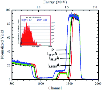 |
| | Fig. 5 Comparison of the RBS spectra of P, I1E15A, I2.5E15A, and I5E15A films. The inset shows the depth distribution of the implanted Fe ions in the CoSb3 thin films. | |
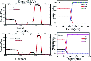 |
| | Fig. 6 Simulated RBS spectra and depth profiles extracted from the RBS analysis of P and I2.5E15A. | |
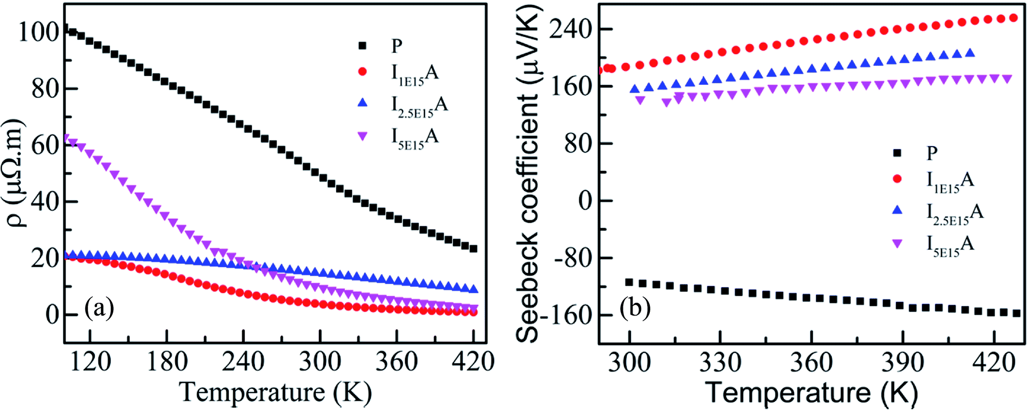
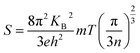
Fig. 7(a) gives the variation of resistivity with temperature for the P, I1E15A, I2.5E15A, and I5E15A films from 100 K to 420 K. The resistivity of all the thin films decreases with the increase in temperature, depicting a typical semiconducting behaviour. However, the resistivity of P (∼100 μΩ m) at 100 K is quite high compared to that of the bulk sample48 (∼8 μΩ m) at the same temperature. The approximate grain size of the films was ∼70–80 nm compared to that of the bulk CoSb3 sample (1–10 μm). Due to the presence of grain boundaries, the scattering effects are enhanced. The high concentration of structural and surface defects also provides a potential barrier for the electrons and increase the resistivity. The resistivity of all implanted films is low compared to that of the pristine film. The resistivity of I1E15A decreases ∼5 times when compared to that of P at low temperature (100 K). It may be due to an increase in the carrier concentration (holes) due to Fe ion implantation. Yang et al.23 reported that the hole concentration in the Fe-doped sample is entirely due to the number of vacancies created by the Fe ion on the Co site in the skutterudite. The TRIM calculation shows the creation of a large number of vacancies (2213.8 per Fe ion), which lead to the increase in the hole concentrations. This greatly assisted in decreasing the electrical resistivity of the Fe-implanted samples. The decrease in resistivity from P to implanted I1E15A can also be explained on the basis of the grain boundary scattering mechanism. From the AFM data, it is observed that the grain size of P increases from 72.4 nm to 95.5 nm for I1E15A. It is generally considered that the samples having a larger grain size must have low electrical resistivity due to the grain boundary scattering mechanism. The resistivity for I5E15A is found to be higher than that for the I1E15A-implanted samples. It may be due to the enhancement of carrier scattering at the grain boundaries because of the presence of the FeSb2 grains. During ion implantation, as the Fe ion fluence increases, the number of vacancies created on the Co site (and hence, the hole concentrations) also increases. Simultaneously, the surface and interstitial defects also increase. These defects and dislocations lead to the decreased mobility of the charge carrier across these defects, which in fact increases in the electrical resistivity at higher fluence. Fig. 7(b) shows the variation of S with temperature for P, I1E15A, I2.5E15A, and I5E15A samples from 300 K to 420 K. The S of the P sample is negative, indicating n-type conduction. However, for the Fe-implanted system, S is positive and shows a p-type conduction behaviour. It has been reported that intrinsic CoSb3 shows n-type and p-type behaviour, depending on the stoichiometry. If pure CoSb3 is synthesised under Co-rich conditions, its behaviour will be n-type as it creates an excess of electrons in the conduction band. If it is synthesised in a Sb-rich environment, it is p-type as this signifies limited Co atoms and leads to the formation of holes in the valence band. In the present study, due to the annealing of films at an elevated temperature of 873 K, some Sb ions are volatilized out, leading to n-type behaviour. For the Fe-implanted samples, Fe (4s23d6) possesses one electron less than Co (4s23d7), so it acts as an acceptor when it occupies the Co site; hence, the Fe-implanted CoSb3 displays p-type conduction behaviour. The electrical properties depend on whether the Fe ion assumes the Fe2+ (3d6) or Fe3+ (3d5) state. The P film gives a S value of −120 μV K−1 at room temperature, which increases up to −157 μV K−1 at 420 K. For the Fe-implanted sample, the S decreases with increasing Fe fluence. The dependency of S on the carrier concentration (n) is given by the relation:
| |
 | (1) |
 |
| | Fig. 7 (a) Resistivity of P, I1E15A, I2.5E15A, and I5E15A. (b) Seebeck coefficient of P, I1E15A, I2.5E15A, and I5E15A. | |
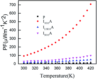
Thus, S depends on the carrier concentration and decreases with increasing ion fluence. The S values for I1E15A, I2.5E15A, and I5E15A at 420 K are 245, 200 and 158 μV K−1, respectively. This is consistent with the results from Yang et al.23 that reported a drop in S with the increase in Fe doping. The decrease in S with increasing fluence may be also due to the generation of a large number of defects created during the implantation process. As the Fe ions enter the material, they create defects in the system. The defects can be present in the form of the implanted ions themselves or the creation of either interstitial or vacancy pairs. These interstitial or vacancy pairs arise due to knock-on collisions, either by the incident ion known as a primary collision or by other knocked-on atoms called a secondary collision. This collision cascade results in a highly disordered region including the defects, and these defects increase with increasing ion fluence. Table 2 compares the S and ρ of the present experimental results with that reported in the literature. From the table, it is evident that the S of the Fe ion-implanted sample is around three times higher than that of the Fe-doped bulk sample. Yang et al.23 also reported that the heat conduction is reduced due to the creation of vacancies on the Co site due to Fe doping. Thus, there is a possibility of dramatically suppressing the lattice thermal conductivity with Fe ion implantation by increasing the lattice defects, mainly by the creation of vacancies on the Co site of the skutterudite structure. Fig. 8 shows the power factor (P.F. = S2/ρ) versus temperature from 300 K to 420 K. The P.F. for the Fe ion-implanted samples are found to be greater than that for the pristine sample. A highest value of P.F. = 700 μW m−1 K−2 is obtained at 420 K for the I1E15A sample. The large increase in P.F. can be attributed to the increase in the carrier concentration, high S and low ρ of the Fe ion-implanted samples.
Table 2 Room temperature Seebeck coefficient and resistivity of the present study compared with that from literature (ref. 23, 46 and 47)
| Sample |
Seebeck coefficient (μV K−1) |
Resistivity (μΩ m) |
| From ref. 46. From ref. 23. From ref. 47. Data from this work. |
| Bulk |
Undoped single crystala |
220 |
18.94 |
| Pristine CoSb3b |
90 |
7 |
| Fe doped (0.5% Fe)b |
60 |
4 |
| Thin film |
Pristine CoSb3c |
∼−6 |
3.2 |
| Pristine CoSb3d |
−120 |
50 |
| Fe doped (this work)d |
187 |
3 |
 |
| | Fig. 8 Power factor of P, I1E15A, I2.5E15A, and I5E15A. | |
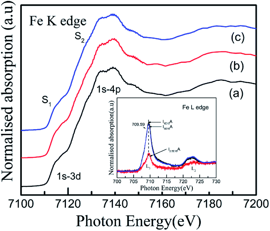
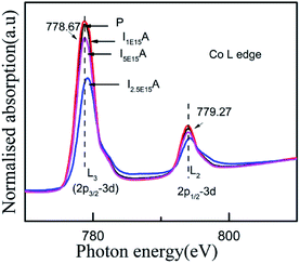
For an in-depth understanding of the structural and electrical properties of the Fe ion-implanted CoSb3, one needs to investigate their electronic structures. Fig. 9 shows the Co L3-edge spectra of the Fe-implanted CoSb3 thin films. These spectra show the splitting of the Co 2p core–hole spin orbit into the L3 (∼779 eV) and L2 (795 eV) edges due to an electron transition from their initial state of 2p3/2 and 2p1/2 to the unoccupied 3d states hybridized with the Sb 5p orbital.49 The peak positions of the L3-edges for P, I1E15A, I2.5E15A, and I5E15A are almost the same within the resolution of this measurement except for I2.5E15A. There is a small shift in the binding energy of I2.5E15A, which shows that the chemical state of the Co ion is different compared to that of P. There is no distinct shoulder peak at 777 eV corresponding to the presence of Co2+ impurities50 (as in CoO). Further, these spectra show a close resemblance to the Co3+ (low spin) EuCoO3 spectra,50 indicating that one can safely rule out the presence of 2+ valence state. This implies that the Co ion in the CoSb6 octahedron is in the 3+ valence state.51 The line shape of the spectrum strongly depends on the multiplet structure formed by the Co 3d–3d and 2p–3d Coulomb and exchange interactions, and also by the local crystal field and hybridization of the Co metal atom with the Sb 5p ligands.11 Due to similar electronegativity between Fe (1.83), Co (1.88) and Sb (2.05), there are four possibilities for the Fe ions to be incorporated into the CoSb3 structure after ion implantation: (i) taking the Sb12 icosahedron voids to form Fe-filled CoSb3, (ii) occupying the Co site in the irregular Sb6 octahedron to form FexCo1−xSb3, (iii) occupying the Sb site in the Sb2Co2 tetrahedron to form CoFexSb3−x or simultaneously occupying the Sb12 icosahedron voids and (iv) substituting the Co site in the irregular Sb6 octahedron. From the figure, the decrease in the intensity of the Co L3-edge is observed for the implanted films as compared to the pristine sample. This decrease in the intensity in the implanted samples indicates that the Fe ions are filled in the Co site. Hence, it is concluded that the Fe ions occupy the Co site in the CoSb6 octahedra. The spectral shapes are almost similar for all the implanted samples, but the width of the white line decreases on the lower energy side of the L3-edge of I2.5E15A. Analysing the full width at half maximum (FWHM) of the spectra, it is observed that the P sample has a FWHM value of 2.87 eV. The FWHM of I1E15A is 3.08 eV and then drops to 2.96 eV, maintaining the same value at higher fluences. After ion implantation, the increase in the FWHM also implies the Fe occupancy of the Co site and the local distortion. Fig. 10 shows the Sb L3-edge of the CoSb3 thin films. The Sb L3-edge arises from the transition from the core 2p3/2 states to the unoccupied 4d and 5s states. The pre-peak marked as S1 in the figure at 4136.62 eV is attributed to the 2p3/2-to-5s transition. The main absorption peak marked as S2 at higher energy, 4145.91 eV, is attributed to the 2p3/2-to-5d transitions.52 A weak shoulder observed in the Sb powder is absent in the pristine sample and implanted thin films. There is an increase in the intensity of the spectral feature of S2 with Fe ion implantation. Consequently, the Fe implantation in the CoSb3 host matrix changes the charge carrier concentration apart from inducing the structural disorder. In the X-ray Absorption Near Edge Structure (XANES) spectra, the absorption features primarily depend on the unoccupied states in the conduction band. Analysis of the spectral features at 4136.62 eV and 4145.91 eV of the Sb L-edge in P (pristine CoSb3) shows an increase in the intensities with Fe ion implantation (for I2.5E15A), indicating an increase of density of unoccupied Sb 5p states. Simultaneously, the Co L-edges of P and I2.5E15A indicate a decrease in the intensities. This implies that there is a charge transfer from Sb to the Co ions due to the Fe ion implantation. In CoSb3, the lowest unoccupied states near the Fermi level are composed of Co 3d and Sb 5p states, and the electrons from these unoccupied states take part in the transport process. Hence, the decrease in resistivity and increase in the Seebeck coefficient for the I2.5E15A sample as compared to P may be attributed to the change in the density of the states contributed by the Co 3d to Sb 5p states. Fig. 11 shows the XANES spectra at the Fe K-edge of the Fe-implanted CoSb3 samples. The XANES pre-edge spectra were analysed by linking spectra from the Fe-implanted samples with those from Fe2O3 and Fe foil. The weak pre-edge peak at ∼7115 eV corresponds to the atomic-like transition from the core 1s orbital to the 3d empty states. The main peaks between 7133 and 7139 eV are associated with a transition from the core 1s orbital to empty 4p states.53 The spectral shape of the I1E15A sample lies at a lower binding energy compared to the samples implanted at higher fluence. The intensity of the main absorption peak at 7133 eV decreases with increasing ion fluence. An additional peak at 7147 eV is also observed in all samples. The pre-edge structure in the XANES spectra of the transition metal Fe K-edge is ascribed to quadrupolar transitions from the core 1s orbital to 3d empty orbitals (dipole forbidden in an ideal octahedron), the transition of the 3d–4p mixing of Co (dipole allowed) and the 3d–p mixing between the Co atom and Sb.54
 |
| | Fig. 9 Co L-edge XANES spectra of the Fe-implanted CoSb3 thin films. | |
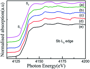 |
| | Fig. 10 Sb L3-edge XANES spectra of the (a) Sb powder, (b) P, (c) I5E15A, (d) I2.5E15A, (e) I1E15A thin films. | |
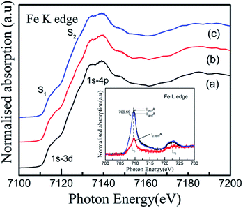 |
| | Fig. 11 Fe K-edge XANES spectra of (a) I1E15A, (b) I2.5E15A, and (c) I5E15A thin films. Inset shows the Fe L3,2-edges XANES spectra of the Fe-implanted CoSb3 thin films. | |
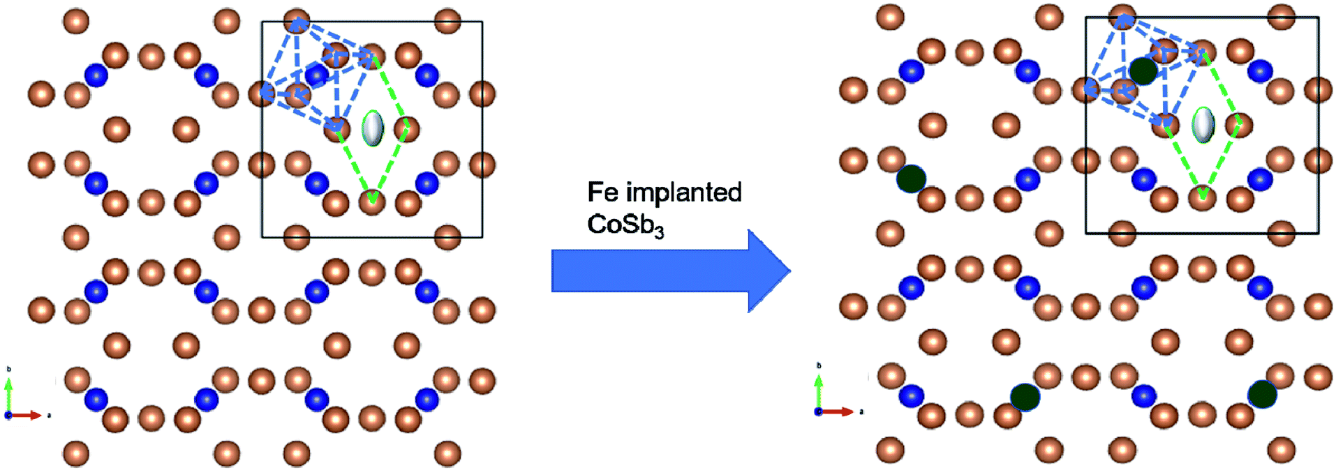
Therefore, the positions of the splitting of the pre-edge peaks directly reflect the crystal field splitting of the 3d orbital sub-bands. For octahedral coordination, the peaks are associated with the t2g and eg transitions. For tetrahedral coordination, the crystal field splitting with the t2g and eg levels is much less and not resolvable into different peaks, so these appear as a single peak. Hence, there is a change in the shape of the pre-edge split peak into a normal singlet peak as the oxidation state changes from a Fe3+ octahedral to a Fe2+ tetrahedral structure. In the present study, the oxidation state for all implanted samples is the 3+ octahedral state. Also, from the small pre-edge feature appearing between 7133 eV and 7138 eV, it can be anticipated that a slightly distorted FeSb6 octahedron is present, indicating that some of the implanted Fe ions substitute Co in the CoSb6 octahedron. Fig. 11 (inset) shows the Fe L3-edge of the Fe-implanted CoSb3 thin films. For divalent iron, the Fe L3-edge spectra are dominated by a sharp peak at 707.8 eV, along with a broader and less intense peak at 710.5 eV. For trivalent iron, the L3-edge is depicted by a sharp peak at 709 eV and a less intense shoulder at 707.8 eV.55 The spectra show the Fe L3-edge at 709.59 eV and a small shoulder at 707 eV. The spectra of the Fe L3-edge of the present study resemble that of the Fe3+ species.55 Hence, the Fe ion is implanted in CoSb3 in the Fe3+ state, which is also confirmed by the Fe K-edge absorption spectra. The pre-edge appears at 7115 eV for the Fe(III) species (as in Fe2O3), and at 7112.5 eV for the Fe(II) species (as in Fe(II) acetate).56 Comparing the pre-edge and main absorption edge features with that of the Fe foil57 and reference iron oxides from literature, these spectra resemble that of the Fe2O3 haematite.56 The absorption pre-edge for all samples appears at 7115 eV, indicating the presence of the Fe3+ species. This is also confirmed from the Fe L-edge spectra. Fig. 12 shows the schematic reflecting the structural modifications due to Fe ion implantations in the CoSb3.
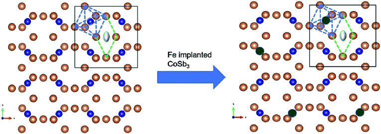 |
| | Fig. 12 Crystal structure of CoSb3. Structure with blue dashed lines forms the CoSb6 octahedra and the one with the green dashed lines depicts the void. Brown-coloured atoms are of Sb, blue ones are of Co and grey-coloured atom shows the guest atom (left). The image (right side) shows the Fe-implanted skutterudite with the Co atom substituted with the Fe atom (green-coloured). | |
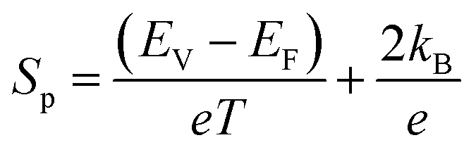
The electrical resistivity decreases substantially after Fe doping, indicating that the Fe ions are electrically active and act as an electron acceptor. This is further confirmed with the changing of the sign of S from a negative value to a positive one after Fe ion implantation. Yang et al.23 reported that the hole concentration increases at a rate of ∼0.03 holes per Fe ion, and concluded that the Fe ions substitute Co in a low spin d5 configuration in the CoSb3 lattice in a trivalent state. Similarly, it can be concluded from the XAS results that the implanted Fe is in the 3+ state. For the implanted samples, the decrease in resistivity is due to the addition of p-type charge carriers. It is observed that the S value decreases with the increase in Fe ion fluence. The lowest fluence (I1E15A) has the highest S value within the complete temperature range. The positive S value follows the relation:58
| |
 | (2) |
where
EV is the minimum of the valence band,
EF is the Fermi level,
e is the charge of the carrier,
kB is the Boltzmann constant, and
T is the absolute temperature. The
S value varies mainly due to the changes in the Fermi level. Due to the doping of Fe ions, the hole carrier concentration increases and shifts the Fermi level towards the valence band; hence, the
S value is positive. In another literature,
11 it is explained that
S is enhanced by Ni ion implantation on the basis of changes in the density of states. Katsuyama
et al.59 reported that FeSb
2 and CoSb
3 form a solid solution. They showed that the electrical resistivity increases and
S decreases due to the presence of FeSb
2 particles. This is consistent with the present study.
4. Conclusion
Polycrystalline CoSb3 thin films with the skutterudite structure were deposited by PLD onto a Si(100) substrate and investigated for their structural, optical, and morphological properties due to Fe ion implantation after RTA. The Fe ion implantation of energy at 120 keV led to the amorphization of films that regained their crystallinity after the RTA process at 873 K. Five out of eight Raman active modes are seen in the samples of PA, I1E15A, and I5E15A, which are absent in the P film, depicting the perfect cubic structure of the as-deposited film. The lattice parameter of the highest-fluence-implanted annealed film is found to correspond to that of the bulk material (9.035 Å). The sign of S changes from negative to positive with Fe doping, giving the highest value of S = 245 μV K−1 for I1E15A at 400 K and the highest value of P.F. (700 μW m−1 K−2). The Fe substitution on the Co site leads to the creation of vacancies, which gives rise to a high concentration of holes. The high Seebeck coefficient and reduced electrical resistivity of the Fe-implanted sample leads to a high power factor. Fe L-edge XANES spectra show that Fe occupies the Co site in the trivalent state. By optimising the parameter of implantation, CoSb3 might lead to advanced thermoelectric applications.
Conflicts of interest
There are no conflicts to declare.
Acknowledgements
The authors (K. A. and A. M.) would like thank the Indo-Taiwan Bilateral Project (Project no.: GITA/DST/TWN/P-64/2015) under the GITA-Department of Science and Technology for providing financial support, including a research fellowship. C. L. D acknowledges both the Taiwan-Indo project of MoST contract number (MoST 104-2923-M-032-001-MY3) and also the Taiwan Experience Education Programs (TEEP) of MoE. We are grateful to Mr Sunil Ojha, Ms Devarani, and Dr Fouran Singh for their help in carrying out the RBS studies, ion implantation, the Raman measurements and research discussions. The authors also thank MRC, MNIT Jaipur for AFM measurements.
References
- M. Rull-Bravo, A. Moure, J. F. Fernández and M. Martín-González, RSC Adv., 2015, 5, 41653–41667 RSC.
- G. S. Nolas, D. T. Morelli and T. M. Tritt, Annu. Rev. Mater. Sci., 1999, 29, 89–116 CrossRef CAS.
- M. V. Daniel, M. Lindorf and M. Albrecht, J. Appl. Phys., 2016, 120, 125306–125311 CrossRef.
- G. S. Nolas, J. Yang and H. Takizawa, Appl. Phys. Lett., 2004, 84, 5210–5212 CrossRef CAS.
- E. Z. Kurmaev, A. Moewes, I. R. Shein, L. D. Finkelstein, A. L. Ivanovskii and H. Anno, J. Phys.: Condens. Matter, 2004, 16, 979–987 CrossRef CAS.
- G. S. Nolas, J. L. Cohn and G. A. Slack, Phys. Rev. B, 1998, 58, 164–170 CrossRef CAS.
- K.-H. Park, S. Lee, W.-S. Seo, S. Baek, D.-K. Shin and I.-H. Kim, J. Korean Phys. Soc., 2014, 64, 1004–1008 CrossRef CAS.
- Z. G. Chen, G. Hana, L. Yanga, L. Cheng and J. Zou, Prog. Nat. Sci.: Mater. Int., 2012, 22, 535–549 CrossRef.
- L. Bertini, C. Stiewe, M. Toprak, S. Williams, D. Platzek, A. Mrotzek, Y. Zhang, C. Gatti, E. Müller, M. Muhammed and M. Rowe, J. Appl. Phys., 2003, 93, 438–447 CrossRef CAS.
- Q. Shen, J. Li and L. Zhang, Sol. Energy Mater. Sol. Cells, 2000, 62, 167–172 CrossRef CAS.
- M. Bala, A. Masarrat, A. Bhogra, R. C. Meena, Y. Lu, Y. Huang, C. Chen, C. Dong, S. Ojha, D. K. Avasthi, S. Annapoorni and K. Asokan, ACS Appl. Energy Mater., 2018, 4–11 Search PubMed.
- M. Bala, A. Bhogra, S. A. Khan, T. S. Tripathi, S. K. Tripathi, D. K. Avasthi and K. Asokan, J. Appl. Phys., 2017, 121, 215301–215309 CrossRef.
- J. Peng, J. Yang, X. Song, Y. Chen, S. Bao and T. Zhang, Front. Mater. Sci. China, 2007, 1, 177–180 CrossRef.
- B. Schüpp, I. Bächer, M. Hecker, N. Mattern, V. Savchuk and J. Schumann, Thin Solid Films, 2003, 434, 75–81 CrossRef.
- K. H. Park and I. H. Kim, Mater. Sci. Forum, 2011, 695, 65–68 CAS.
- X. Zhang, Q. M. Lu, J. X. Zhang, Q. Wei, D. M. Liu and Y. Q. Liu, J. Alloys Compd., 2008, 457, 368–371 CrossRef CAS.
- G. A. Lamberton Jr, S. Bhattacharya, R. T. Littleton IV, M. A. Kaeser, R. H. Tedstrom, T. M. Tritt, J. Yang and G. S. Nolas, Appl. Phys. Lett., 2002, 80, 598–600 CrossRef.
- X. Shi, S. Bai, L. Xi, J. Yang, W. Zhang, L. Chen and J. Yang, J. Mater. Res., 2011, 26, 1745–1754 CrossRef CAS.
- G. Meisner, D. Morelli, S. Hu, J. Yang and C. Uher, Phys. Rev. Lett., 1998, 80, 3551–3554 CrossRef CAS.
- G. S. Nolas, M. Kaeser, R. T. Littleton and T. M. Tritt, Appl. Phys. Lett., 2000, 77, 1855–1857 CrossRef CAS.
- S. Wang, J. R. Salvador, J. Yang, P. Wei, B. Duan and J. Yang, NPG Asia Mater., 2016, 8, e285 CrossRef CAS.
- X. Shi, J. Yang, J. R. Salvador, M. F. Chi, J. Y. Cho, H. Wang, S. Q. Bai, J. H. Yang, W. Q. Zhang and L. D. Chen, J. Am. Chem. Soc., 2011, 133, 7837–7846 CrossRef CAS.
- J. Yang, G. P. Meisner, D. T. Morelli and C. Uher, Phys. Rev. B, 2000, 63, 1–11 Search PubMed.
- S. Katsuyama, Y. Shichijo, M. Ito, K. Majima and H. Nagai, J. Appl. Phys., 1998, 84, 6708–6712 CrossRef CAS.
- Il-Ho Kim and S-C. Ur, Mater. Lett., 2007, 61, 2446–2450 CrossRef.
- V. Savchuk, A. Boulouz, S. Chakraborty, J. Schumann and H. Vinzelberg, J. Appl. Phys., 2002, 92, 5319–5326 CrossRef CAS.
- M. V. Daniel, C. Brombacher, G. Beddies, N. Jöhrmann, M. Hietschold, D. C. Johnson, Z. Aabdin, N. Peranio, O. Eibl and M. Albrecht, J. Alloys Compd., 2015, 624, 216–225 CrossRef CAS.
- S. R. Sarath Kumar, A. Alyamani, J. W. Graff, T. M. Tritt and H. N. Alshareef, J. Mater. Res., 2011, 26, 1836–1841 CrossRef.
- S. R. S. Kumar, D. Cha and H. N. Alshareef, J. Appl. Phys., 2011, 110, 083710 CrossRef.
- S. Yadav, S. Chaudhary and D. K. Pandya, Appl. Surf. Sci., 2018, 435, 1265–1272 CrossRef CAS.
- L. Kumari, W. Li, J. Y. Huang and P. P. Provencio, Nanoscale Res. Lett., 2010, 5, 1698–1705 CrossRef CAS.
- H. Anno, T. Sakakibara, Y. Notohara, H. Tashiro, T. Koyanagi, H. Kaneko and K. Matsubara, XVI ICT'97, Proc. ICT'97, 16th Int. Conf. Thermoelectr. (Cat. No.97TH8291), 1997, vol. 81, pp. 338–342 Search PubMed.
- A. Ahmed and S. Han, Appl. Surf. Sci., 2017, 408, 88–95 CrossRef CAS.
- S. R. Sarath Kumar, D. Cha and H. N. Alshareef, J. Appl. Phys., 2011, 110, 083710 CrossRef.
- J. C. Caylor, A. M. Stacy, R. Gronsky and T. Sands, J. Appl. Phys., 2001, 89, 3508–3513 CrossRef CAS.
- A. Dauscher, M. Puyet, B. Lenoir, D. Colceag and M. Dinescu, Appl. Phys. A, 2004, 79, 1465–1468 CrossRef CAS.
- D. Colceag, A. Dauscher, B. Lenoir, V. Da Ros, R. Birjega, A. Moldovan and M. Dinescu, Appl. Surf. Sci., 2007, 253, 8097–8101 CrossRef CAS.
- T. S. Tripathi, M. Bala and K. Asokan, Rev. Sci. Instrum., 2014, 85, 085115 CrossRef CAS.
- W. Möller and W. Eckstein, Nucl. Instrum. Methods Phys. Res., Sect. B, 1984, 814–818 CrossRef.
- E. N. M. Christensen, B. B. Iversen, L. Bertini, C. Gatti, M. Toprak and M. Muhammed, J. Appl. Phys., 2004, 96, 3148–3157 CrossRef.
- K. Momma and F. Izumi, J. Appl. Crystallogr., 2011, 44, 1272–1276 CrossRef CAS.
- P. Wei, W. Zhao, D. Tang, W. Zhu, X. Nie and Q. Zhang, J. Mater., 2016, 2, 280–289 Search PubMed.
- G. S. Nolas, C. A. Kendziora and H. Takizawa, J. Appl. Phys., 2003, 94, 7440–7444 CrossRef CAS.
- J. L. Feldman and D. J. Singh, Phys. Rev. B, 1996, 53, 6273–6282 CrossRef CAS.
- J. F. Ziegler, M. D. Ziegler and J. P. Biersack, Nucl. Instrum. Methods Phys. Res., Sect. B, 2010, 268, 1818–1823 CrossRef CAS.
- T. Caillat, A. Borshchevsky and J.-P. Fleurial, J. Appl. Phys., 1996, 80, 4442–4449 CrossRef CAS.
- M. Bala, S. Gupta, S. K. Srivastava, S. Amrithapandian, T. S. Tripathi, S. K. Tripathi, C. Dong, C. Chen, D. K. Avasthi and K. Asokan, Phys. Chem. Chem. Phys., 2017, 19, 24886–24895 RSC.
- J. W. Sharp, E. C. Jones, R. K. Williams, P. M. Martin and B. C. Sales, J. Appl. Phys., 1995, 78, 1013–1018 CrossRef CAS.
- C.-J. Liu, J.-L. Chen, L.-C. Huang, Z.-R. Lin and C.-L. Chang, J. Appl. Phys., 2007, 102, 014908 CrossRef.
- S. Y. Istomin, O. A. Tyablikov, S. M. Kazakov, E. V Antipov, A. I. Kurbakov, A. A. Tsirlin, N. Hollmann, Y. Y. Chin, H. Lin, C. T. Chen, A. Tanaka, L. H. Tjeng and Z. Hu, Dalton Trans., 2015, 44, 10708–10713 RSC.
- T. Burnus, Z. Hu, M. W. Haverkort, J. C. Cezar, D. Flahaut, V. Hardy, A. Maignan, N. B. Brookes, A. Tanaka, H. H. Hsieh, H.-J. Lin, C. T. Chen and L. H. Tjeng, Phys. Rev. B: Condens. Matter Mater. Phys., 2006, 74, 245111–245115 CrossRef.
- D. F. Franco, H. Fares, A. E. De Souza, S. H. Santagneli and M. Nalin, Ecletica Quim. J., 2017, 42, 51–59 CrossRef.
- M. G. Kim, H. S. Cho and C. H. Yo, J. Phys. Chem. Solids, 1998, 59, 1369–1381 CrossRef CAS.
- T. Yamamoto, X-Ray Spectrom., 2008, 37, 572–584 CrossRef CAS.
- P. A. van Aken, B. Liebscher and V. J. Styrsa, Phys. Chem. Miner., 1998, 4, 323–327 CrossRef.
- C. Genovese, M. E. Schuster, E. K. Gibson, D. Gianolio, V. Posligua, R. Grau-crespo, G. Cibin, P. P. Wells, D. Garai, V. Solokha, S. K. Calderon, J. J. Velasco-velez, C. Ampelli, S. Perathoner, G. Held, G. Centi and R. Arrigo, Nat. Commun., 2018, 9, 1–12 CrossRef CAS.
- Z. Guo, L. L. Henry and E. J. Podlaha, J. Mater. Chem., 2005, 16, 1772–1777 RSC.
- R. C. Mallik, R. Anbalagan, G. Rogl, E. Royanian, P. Heinrich, E. Bauer, P. Rogl and S. Suwas, Acta Mater., 2013, 61, 6698–6711 CrossRef CAS.
- S. Katsuyama, Y. Kanayama, M. Ito, K. Majima and H. Nagai, J. Appl. Phys., 2000, 88, 3484–3489 CrossRef CAS.
|
| This journal is © The Royal Society of Chemistry 2019 |
Click here to see how this site uses Cookies. View our privacy policy here. 
 Open Access Article
 This Open Access Article is licensed under a Creative Commons Attribution-Non Commercial 3.0 Unported Licence
 c,
Ranveer Singhd,
Vineet Barwale,
Chung-Li Dong
c,
Ranveer Singhd,
Vineet Barwale,
Chung-Li Dong