
 Open Access Article
 This Open Access Article is licensed under a Creative Commons Attribution-Non Commercial 3.0 Unported Licence
Tuning the orientation of few-layer MoS2 films using one-zone sulfurization
Michaela Sojková *a,
Karol Vegsobc,
Nada Mrkyvkovabc,
Jakub Hagarab,
Peter Hutára,
Alica Rosováa,
Mária Čaplovičovád,
Ursula Ludackae,
Viera Skákalováde,
Eva Majkovábc,
Peter Siffalovicbc and
Martin Hulmana
*a,
Karol Vegsobc,
Nada Mrkyvkovabc,
Jakub Hagarab,
Peter Hutára,
Alica Rosováa,
Mária Čaplovičovád,
Ursula Ludackae,
Viera Skákalováde,
Eva Majkovábc,
Peter Siffalovicbc and
Martin Hulmana
aInstitute of Electrical Engineering, SAS, Dúbravská Cesta 9, 84104 Bratislava, Slovakia. E-mail: michaela.sojkova@savba.sk
bInstitute of Physics, SAS, Dúbravská Cesta 9, 84511 Bratislava, Slovakia
cCentre for Advanced Materials Application, Dúbravská Cesta 9, 84511 Bratislava, Slovakia
dSTU Centre for Nanodiagnostics, Vazovova 5, 81243 Bratislava, Slovak Republic
eUniversity of Vienna, Faculty of Physics, Boltzmanngasse 5, 1090 Vienna, Austria
First published on 19th September 2019
Abstract
Few-layer MoS2 films are promising candidates for applications in numerous areas, such as photovoltaics, photocatalysis, nanotribology, lithium batteries, hydro-desulfurization catalysis and dry lubricants, especially due to their distinctive electronic, optical, and catalytic properties. In general, two alignments of MoS2 layers are possible – the horizontal and the vertical one, having different physicochemical properties. Layers of both orientations are conventionally fabricated by a sulfurization of pre-deposited Mo films. So far, the Mo thickness was considered as a critical parameter influencing the final orientation of MoS2 layers with horizontally and vertically aligned MoS2 grown from thin (1 nm) and thick (3 nm) Mo films, respectively. Here, we present a fabrication protocol enabling the growth of horizontally or vertically aligned few-layer MoS2 films utilizing the same Mo thickness of 3 nm. We show that the sulfur vapor is another parameter influencing the growth mechanism, where a sulfurization with higher sulfur vapor pressure leads to vertical MoS2 layers and slow sulfur evaporation results in horizontally aligned layers for a thicker Mo starting layer.
Introduction
MoS2, a semiconducting analog of graphene, is one of the most studied members of the transition metal dichalcogenide (TMD) family. The properties of TMD materials make them highly attractive for fundamental studies of novel physical phenomena and applications ranging from nanoelectronics and nanophotonics to sensing and actuation at the nanoscale. TMD materials with a layered structure have a general formula MX2, where M refers to a transition metal and X refers to a chalcogen (S, Se, or Te).1 In the case of MoS2, there is a strong ionic bonding between sulfur and molybdenum atoms while the different layers of MoS2 interact via van der Waals (vdW) forces.2 Some of the TMD materials with hexagonal structure has the ability to grow with vertical or horizontal alignment. Various fabrication methods such as exfoliation of bulk crystals,3–6 chemical vapor deposition7–9 or pulsed laser deposition10–12 can be used to produce MoS2 monolayers or few-layers films. Depending on the fabrication conditions, MoS2 layer can grow with basal planes aligned horizontally or vertically. The basal planes are oriented parallel to the substrate surface and the crystallographic c-axis is aligned along the substrate surface normal in the horizontal alignment. On the other hand, the basal planes are standing upright on the substrate and the c-axis is perpendicular to the surface normal for the vertical alignment. Besides of MoS2, vertically aligned layers of WS2,13,14 WSe2 (ref. 15) and PtSe2 (ref. 16 and 17) layers were prepared recently.The spatial orientation of MoS2 layers is important for anticipated applications of this material. Horizontally aligned (HA) MoS2 films are suitable for optoelectronics3,18,19 and electronics.20–22 Vertically aligned (VA) MoS2 films are of special interest as they can be utilized for hydrogen evolution reaction (HER),23,24 water disinfection,25,26 water splitting27 or solar cells28,29 due to the chemically reactive edge sites. Among the approaches leading to VA MoS2 layers, solution-based methods use the decomposition of dissolved molybdenum compounds by microwaves30 or hydrothermal reaction.26,31 Also thermolysis of molybdenates can offer VA MoS2 under specific conditions. However, the most common technique is a two-zone sulfurization of the molybdenum films. This method was applied for the first time by Jäger-Waldau et al.32 and they showed that the sulfur temperature is a key parameter for the fabrication of MoS2 thin films. Even though, sulfurization is quite simple and straightforward technique to prepare VA films,13,25,33–35 the growth mechanism is still not fully clear. Kong et al.34 and Gaur et al.35 proposed that the competition among growth and nucleation under a given set of conditions is crucial in the vertical and lateral growth of 2D islands. This suggests that thermodynamics and diffusion play an important role in the synthesis of thin layers. Jung et al.13 studied the growth of VA MoS2 and WS2. They found out that the thickness of the initial molybdenum/tungsten layer is a critical parameter determining the growth directions. Using thicker (≳3 nm) Mo/W layers, the vertical growth is dominant, while the horizontal growth occurs in thinner layers. They suppose the following explanation – the sulfurization of Mo/W layers is connected with a significant volume expansion. For very thin and discontinuous Mo/W layers, the growth of large-area 2D HA films is energetically more favorable over the growth of VA layers. For thicker and continuous films, as the metal seed layer is anchored to the substrates, horizontal volume expansion is hard to realize.13 A similar mechanism is proposed also for PtSe2 films grown by rapid selenization.16 Shang et al.36 proposed a mechanism controlling vertical versus lateral growth of 2D MoS2 islands where the thermodynamic growth window is guiding the deposition of MoS2 thin films. They pointed out that the key factors that control the growth of MoS2 includes temperature, pressure, substrate and chemical potentials. In addition to thermodynamics, the performed DFT calculations suggested that Mo diffusion is a controlling factor for MoS2 growth owing to an extremely low Mo diffusivity compared to that of sulfur.36 Recently, Choudhary et al.37 studied the CVD growth mechanism of 2D molybdenum/tungsten disulfide vertical stacks grown on the tungsten trioxide (WO3) nanowires using transmission electron microscopy. MoS2 layers of different thickness were prepared using HA WS2 layers as a substrate. They confirmed that the relaxation of the strain energy built up during growth guides the 2D layers orientation and determines the growth mode dictated by the thickness of Mo. They observed that 2D MoS2 layers are growing from the interface of the Mo–WS2 basal plane in a “bottom-to-top” manner. Moreover, they found out that in the case of VA layers, two competing kinetic factors, i.e., sulfurization kinetics of deposited metals versus growth kinetics of 2D layers driven by the metal (Mo)-substrate interfacial energy, have to be considered. They confirmed that 2D layer growths can also occur on the “top” surface if their thickness is large enough. The sulfurization kinetics on the film surface locally dominates the growth kinetics on the growth substrate.
In the literature, VA MoS2 are frequently connected to rapid sulfurization in a two-zone furnace.13,25,33–35 In most cases, Si/SiO2 was used as a substrate, but the growth on other substrates including glassy carbon, sapphire and quartz was also reported. Typically, the annealing temperature was in the ranges from 500 to 800 °C and a short annealing time (10–20 min) was applied. The common feature of these works is a fast heating rate in order of tens degrees centigrade per minute. Moreover, VA MoS2 is formed when the thickness of Mo film exceeds 3 nm making the thickness one of the critical growth parameters. However, the effect of the heating rate is by far less explored. Stern et al.38 prepared MoS2 from 70 nm thick Mo layer using two different heating rates (20 °C min−1 and 5 °C min−1). They observed a gradual transition from the disordered crystalline MoS2 to vertically oriented morphology. Therefore, the heating rate seems to be another important factor influencing the orientation of MoS2 films.
Here, we present a growth method leading to HA or VA MoS2 films by sulfurizing Mo films with the same thickness (3 nm). By decreasing the heating rate, we observed the transition from the vertical to horizontal layer alignment. To acquire a complete picture, we also studied the effect of the process temperature, substrate and heating rate on the MoS2. Based on the results obtained we conclude that the amount of the sulfur during the growth process and the diffusion controls the final alignment of a thin MoS2 layer.
Results and discussion
Fig. 1a shows Raman spectra of MoS2 layers grown from 1 nm thick Mo films at temperatures from 350 to 800 °C. By increasing the annealing temperature, the spacing between the A1g and E12g Raman modes (Δf) increased from 23.1 to 24.7 cm−1 (Fig. 1b). The thickness of the as-grown MoS2 is expected to be 3.5 times larger than that of the initial pristine Mo layer.13,39 Thus, for 1 nm Mo layer, the MoS2 thickness should be about 3.5 nm corresponding to 5–6 monolayers. On the other hand, the results from Raman measurements suggests that the number of MoS2 monolayers increases from 2 to more than 5 with the increasing annealing temperature.10 Presumably, only the topmost part of the Mo layer gets sulfurized at lower temperatures. By increasing the annealing temperature, the reaction of sulfur and Mo propagates deeper into the Mo layer and the number of MoS2 layers successively increases. Fig. 1b also shows the linewidths of the two Raman modes. Both, they exhibit a similar trend with the linewidth getting narrower as the deposition temperature increases from 350 °C to 800 °C. Analogous to Δf, two regions with a different temperature dependence can also be recognized for the linewidth. The latter is almost temperature independent for temperatures up to 500 °C. At even higher deposition temperatures, the Raman peaks become gradually narrower reaching the values of 6.2 and 6.4 cm−1 for the E12g and A1g modes, respectively. We assume the change of the linewidth is related to improving the layer crystallinity in terms of the size of MoS2 crystallites. It is known that a Raman linewidth is a sensitive probe characterising length scales in spatially confined systems.40 A chemical state and composition of as prepared films were analyzed by XPS spectroscopy (Fig. 2). The Mo 3d region exhibits two characteristic emission peaks at 231.84 eV (Mo 3d3/2) and 228.75 eV (Mo 3d5/2). These binding energy values are consistent with charge state corresponding to MoS2.41 Additionally, the S 2s peak at a binding energy of 226.12 eV corresponding to MoS2 is also observed41 in this spectral region.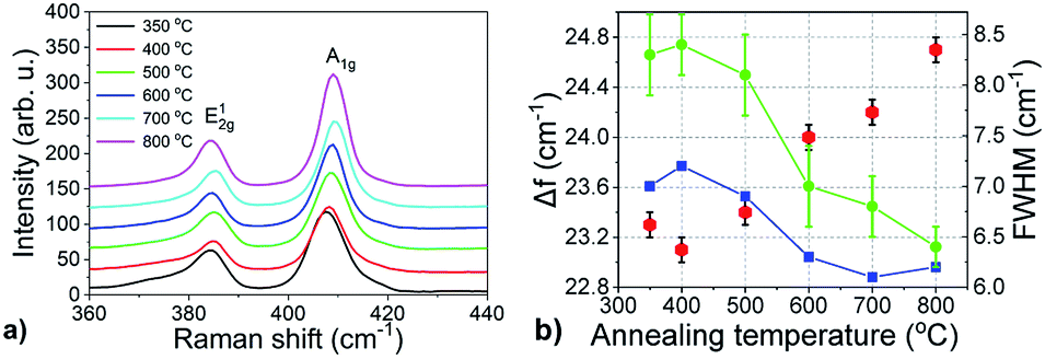 | ||
| Fig. 1 (a) Raman spectra of MoS2 layers grown from a 1 nm thick Mo film on the c-plane sapphire substrate at different temperatures. (b) Dependence of the spacing, Δf, between the A1g and E12g Raman modes (red points) and the linewidth (A1g – green points and E12g – blue points) on the annealing temperature. | ||
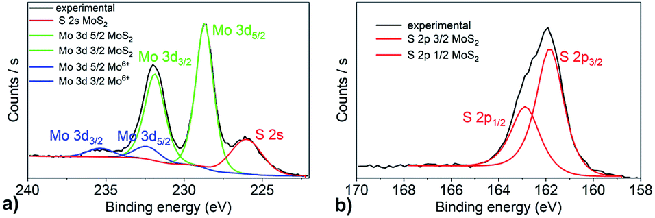 | ||
| Fig. 2 XPS spectra of the MoS2 layer grown on sapphire at 800 °C/30 min from a 3 nm thick Mo film. The binding energies of Mo 3d and S 2p core-level states are displayed in panels (a) and (b), respectively. | ||
The spin–orbit energy splitting of the Mo 3d doublet is 3.1 eV, which is in good agreement with previous reports.42,43 The S 2p spectrum (Fig. 2b) contains spin–orbit doublets of S 2p3/2 centered at 161.92 eV and S 2p1/2 at 162.9 eV, with a spin–orbit splitting of 0.98 eV. No Mo 3d doublet at the binding energies of 231.4 eV and 228.4 eV corresponding to the elemental Mo0 state was observed. However, a limited contribution attributed to the presence of MoO3 was identified at the binding energies of 232.45 eV and 235.4 eV for Mo 3d5/2 and Mo 3d3/2 core-level states, respectively (Fig. 2a). No peaks corresponding to S 2p in SO3 (Fig. 2b) were found. Quantification of the peak areas provides the atomic concentrations of S and Mo in single compounds. The Mo4+ state in MoS2 reaches almost 90% and sulfur S2− state is close to 100%. As expected, the calculated S/Mo ratio is close to 2.
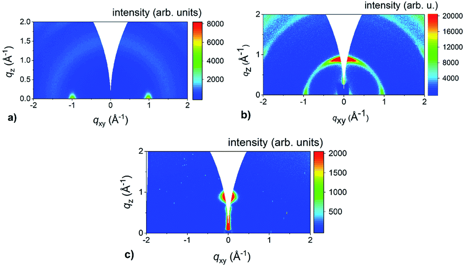
To find out the orientation of the as-prepared MoS2 films, GIWAXS measurements were performed. This method is useful for studying the crystallographic orientation of thin polycrystalline films.44 GIWAXS provides a statistical average over significant section of the sample surface in contrast to HRTEM, which probes the sample locally. Furthermore, no special sample preparation is required for the GIWAXS measurements. GIWAXS patterns of 1 and 3 nm thick Mo films sulfurized at 400 °C and 800 °C for 30 min are shown in Fig. 3. The fuzzy background was caused by the use of the image plate detector. The heating rate was 25 °C min−1 in all these experiments. For thin MoS2 samples (grown from 1 nm of Mo), an intense 002 diffraction of MoS2 is located at qz = 1 Å−1. MoS2 layers exhibit a uniaxial texture with the crystallographic c-axis aligned along the substrate surface normal (Fig. 3a and c). For the layers grown from 3 nm thick Mo films, two 002 diffraction spots are detected at qxy = 1 Å−1 and the c-axis is now perpendicular to the surface normal (Fig. 3c and d). It is obvious that the VA MoS2 films were grown from 3 nm Mo layers even at the lowest annealing temperature. We observed the same behavior using longer annealing time (up to 48 h, not shown here). This suggests that the formation of VA MoS2 is influenced neither by the annealing temperature nor time but just by the Mo film thickness when the samples were rapidly heated up during their growth.
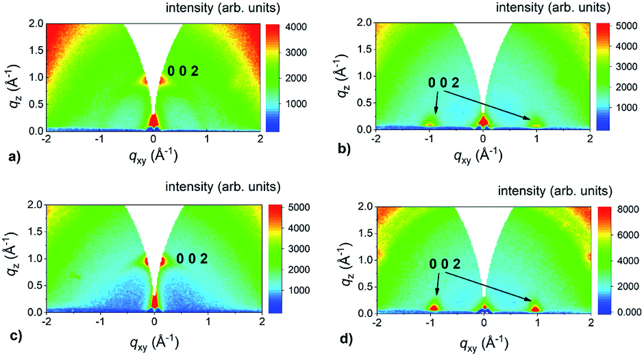 | ||
| Fig. 3 GIWAXS reciprocal space maps of MoS2 layers prepared from Mo films with the nominal thickness of (a) 1 nm and (b) 3 nm sulfurized at 400 °C/30 min and (c) 1 nm and (d) 3 nm sulfurized at 800 °C/30 min. | ||
To check whether this growth mode is specific only for c-sapphire substrate, we grew MoS2 layers on other substrates, too. We used chemically inert GaN (gallium nitride) as well as reactive GaP (gallium phosphide) and microcrystalline CVD diamond substrates. In all cases, MoS2 layers grown from the 1 nm Mo are aligned horizontally. The use of the thicker 3 nm films (6 nm in the case of the diamond substrate because of shadowing effect45) led to VA MoS2 films for all the substrates. GIWAXS reciprocal space maps of MoS2 layers prepared from 3 nm (GaN, GaP) and 6 nm (diamond) thick Mo layers and shown in Fig. 4 confirm that the choice of the substrate has no effect on the MoS2 orientation. In the special case of the diamond substrate, also the diffraction ring at q ∼ 3 Å−1 belonging to 111 diffraction of diamond and two less intense 100 and 103 diffractions of MoS2 at 2.3 and 2.7 Å−1 are visible (Fig. 4c). The apparent moderate orientation degree of the crystallographic c-axis has an origin in large angular spread of the underlying polycrystalline diamond facets.45
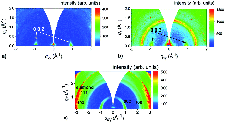 | ||
| Fig. 4 GIWAXS reciprocal space maps of MoS2 layers prepared on (a) GaN (from 3 nm Mo), (b) chemGaP (from 3 nm Mo) and (c) microcrystalline CVD diamond (from 6 nm Mo) substrates. | ||
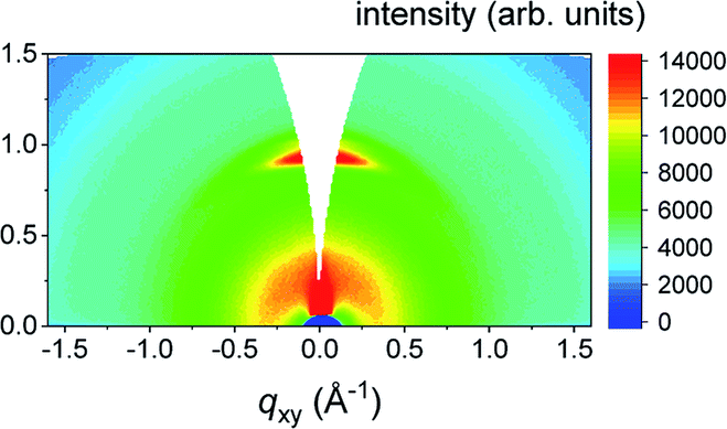
To elucidate whether the VA MoS2 growth of the is linked only with the rapid sulfurization, we grew MoS2 layers changing the heating rate and measured the layer alignment. The heating rate values were altered from 25 °C min−1 down to 0.5 °C min−1. The sulfurization temperature and duration were kept constant at 800 °C and 30 min, respectively.
It is evident from Fig. 5 that the heating rate had a significant impact on the layer alignment of thicker MoS2 films. By decreasing the heating rate, the orientation of the films changes from the VA (Fig. 5a) through a mixed state with combined VA and HA (Fig. 5b) to HA films (Fig. 5c). In addition to the Mo thickness, the heating rate is another process parameter for controlling the layer alignment. This indicates that the amount of the sulfur reaching the pre-deposited Mo substrate plays a key role in the sulfurization mechanism. Since the sulfur melts at low temperature (∼115 °C), all the sulfur is very likely consumed at the early stages of the sulfurization at temperatures lower than the final one at 800 °C. Thus, the heating rate determines the sulfur vapor partial pressure during the synthesis, which is higher for rapid sulfurization and lower for the slow heating rate of 0.5 °C min−1. Following this line of reasoning, we performed another experiment when the nitrogen flow through the CVD chamber was increased 5-fold during a rapid sulfurization growth. The aim was to reduce the amount of sulfur in the chamber by another way. The GIWAXS result shown in Fig. 6 confirms the horizontal alignment of the as-grown layer. Based on this, the following scenario for the growth mechanism emerges from our experiments. We follow the proposal of Choudhary et al.37 that MoS2 layers are growing horizontally from the Mo-substrate interface in the bottom-to-top manner. However, if a concentration of sulfur atoms exceeds a certain critical value, the sulfurization may start on or near the surface of the Mo film where the concentration is highest. In such a case a MoS2 layer seems to prefer vertical alignment. The concentration can be reduced below the critical one either by reducing the amount of sulfur supplied or by diffusion the sulfur atoms into the Mo film. We tested the former possibility by slowing down the heating rate and reducing the sulfur vapor concentration. It is assumed that the diffusion rate of the sulfur atoms is responsible for the observed dependence of the layer alignment on the thickness. It is known that sulfur atoms diffuse rather slowly into molybdenum46,47 so in the thicker layer the critical concentration is reached on the film surface and triggers vertical growth of MoS2 before the atoms reach the Mo-substrate interface.
 | ||
| Fig. 5 GIWAXS reciprocal space maps of MoS2 films on the c-plane sapphire substrate prepared from 3 nm thick Mo layers at 800 °C during 30 min with the heating rate of (a) 25 °C min−1, (b) 5 °C min−1 and (c) 0.5 °C min−1. The peaks at ∼1 Å−1 originate from the (002) diffraction planes. | ||
 | ||
| Fig. 6 GIWAXS reciprocal space maps of MoS2 films on the c-plane sapphire substrate prepared from 3 nm thick Mo layers at 800 °C during 30 min with the heating rate of 25 °C min−1 using 5 times higher nitrogen flow. | ||
The experiments with the lower heating rates were also performed at the lower sulfurization temperature (400 °C). The transition from the vertical to horizontal alignment was observed for the 3 nm thick Mo layers exactly as in the case of the sulfurization at 800 °C. The lower partial sulfur pressure lead to horizontal MoS2 growth even in the low temperature sulfurization.
The MoS2 films prepared at the decreased heating rates were also studied by Raman spectroscopy (Fig. 7). An increase of the E12g intensity relative to the A1g one was observed when the heating rate was reduced from 25 °C min−1 down to 0.5 °C min−1. Kong et al.34 reported, that based on the peak intensities, it is possible to estimate the texture of the film. Raman peak corresponding to out-of-plane Mo–S phonon mode (A1g) is preferentially excited for the edge-terminated film due to the polarization dependence, whereas the in-plane Mo–S phonon mode (E12g) is preferentially excited for the terrace-terminated film. In the case of vertically aligned layers, E12g peak is smaller having just 30% of the intensity of A1g peak.34 The increase of the E12g is consistent with the vertical to horizontal transition observed in the GIWAXS measurements. In addition to this, the linewidth of the Raman peaks gets narrow for a slowly sulfurized sample indicating its better crystallinity compared to the samples sulfurized more rapidly.
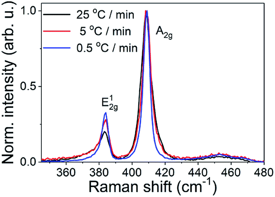 | ||
| Fig. 7 Raman spectra of MoS2 films prepared from 3 nm thick Mo at 800 °C/30 min with the heating rate of 25 °C min−1, 5 °C min−1 and 0.5 °C min−1. | ||
Finally, a TEM analysis was performed to confirm the MoS2 orientation and compare the results with those from the GIWAXS measurements. Three samples have been analyzed – HA MoS2 prepared from 1 nm and 3 nm thick Mo films and VA MoS2 prepared from a 3 nm thick Mo film. Fig. 8 shows a HRTEM image of a MoS2 layer prepared from a 3 nm thick Mo film by rapid sulfurization. Most of MoS2 layers seen in the figure are vertically aligned. The distance between the fringes correspond to that of {002} crystal planes (d = 0.6155 nm), however, periodic fringes belonging to {100} (d = 0.2738 nm) and {103} (d = 0.2277 nm) crystal planes can also be observed due to a mutual mis-orientation of some MoS2 grains. A layer prepared by rapid sulfurization of 1 nm Mo layer (Fig. 9) is poly-crystalline with no VA layers present. As it can be seen in Fig. 9a, the sample contains both well-ordered parts (red box, left) and parts with some rotational mis-orientation in the layer of horizontally-grown MoS2, as indicated by an appearance of typical two-dimensional Moiré patterns (blue box, right). In the case of the well-ordered part, it is not possible to estimate the number of monolayers. However, it is clear that at least two monolayers are present in the rotationally mis-oriented parts. A Fast Fourier Transformation (FFT) image taken from the part with the Moiré pattern confirms the superposition of rotationally mis-oriented MoS2 sheets (Fig. 9c). The transition from a vertical to horizontal alignment for a thick MoS2 layer prepared from a 3 nm Mo film was confirmed also by the STEM measurements. A multilayered HA MoS2 film with no indication of VA phase can be seen in Fig. 10. Compared to the result shown in Fig. 9, the thick HA MoS2 layer is less ordered than the thinner one prepared by sulfurization of a 1 nm thick Mo film.
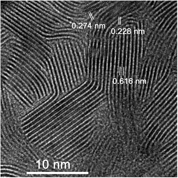 | ||
| Fig. 8 HRTEM image of MoS2 layer prepared from 3 nm Mo at 800 °C during 30 min with heating rate of 25 °C min−1. | ||
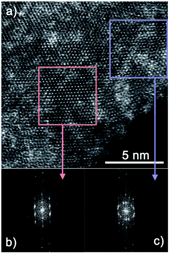 | ||
| Fig. 9 STEM image using HAADF (high-angle annular dark-field) detector of MoS2 layer prepared from 1 nm thick Mo at 800 °C during 30 min with heating rate of 25 °C min−1 (a) and FFT images from the selected zones (b and c). | ||
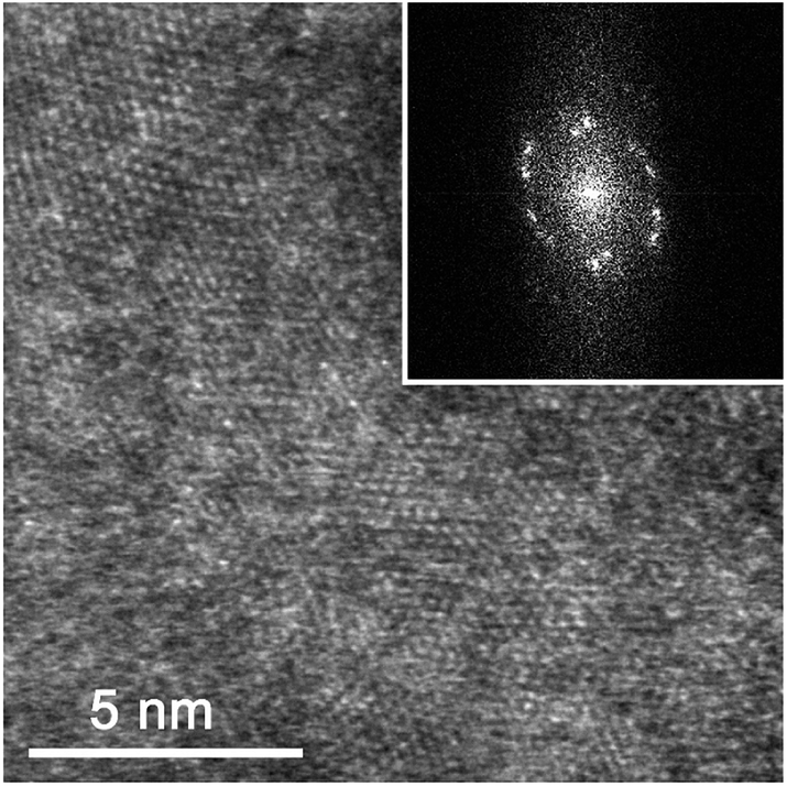 | ||
| Fig. 10 STEM image using HAADF detector of a MoS2 layer prepared from a 3 nm thick Mo film at 800 °C by a slow rate sulfurization during 30 min with the heating rate of 0.5 °C min−1. The inset shows a FFT of the STEM image. | ||
Conclusions
Fabrication of large-area MoS2 layers with a controllable orientation is an important issue. We presented a simplified sulfurization technique, where Mo coated substrates and a sulfur powder are placed close to each other in a one-zone furnace and exposed to the same temperature without additional control over the sulfur temperature. We showed that in the case of rapid sulfurization (heating rate of 25 °C min−1) the thickness of a pre-deposited Mo film is a critical parameter determining the orientation of the final MoS2 layer. Horizontally and vertically aligned layers were grown from a Mo film with an initial thickness of 1 nm and 3 nm, respectively. By reducing the heating rate, the orientation of the films is changing from the vertical one (25 °C min−1) through a mixed state with combined vertical and horizontal alignment (5 °C min−1) to horizontally aligned layers (0.5 °C min−1) even for 3 nm thick Mo. A similar transition was also observed when the amount of sulfur reacting with Mo during the layer growth was reduced. This points out that the atomic flux of sulfur and (likely) its diffusion rate into Mo are other parameters controlling the MoS2 layer alignment. On the other hand, we found out that other parameters such as annealing temperature, time of the sulfurization as well as the substrate have no influence on the alignment of MoS2 layers. The presented method opens up the possibility for the growth of heterostructures with HA and VA aligned MoS2 layers placed one on top of the other.Methods
MoS2 fabrication
MoS2 thin films were prepared by a two-step method. At first, DC magnetron sputtering in Ar atmosphere (10−3 mbar) from a Mo target at room temperature was used for the fabrication of Mo seed layers. The DC power and emission current were set to 140 W and 0.3 A, respectively. The thickness of the as-prepared Mo films (1 and 3 nm) was controlled by the rotation speed of a sample holder and verified by atomic force microscopy (AFM) carried out on NT-MDT NTegra Aura in a semi-contact mode on the patterned Mo films. Further, the pre-deposited Mo layers were sulfurized in a custom-designed CVD chamber. The growth takes place in a one-zone furnace with a sulfur powder (0.5 g) placed along with the seed Mo film in the center of the furnace. In particular, Mo layer was annealed in sulfur vapors at temperatures from 350 to 800 °C in N2 atmosphere at ambient pressure. The annealing time ranged from 5 minutes to 48 hours.Chemical composition analyses
Raman measurements were performed with a confocal Raman microscope (Alpha 300 R, WiTec, Germany) using a 532 nm excitation laser wavelength. The laser power was kept as low as 1 mW to avoid any beam induced damage. The scattered Raman signal was collected by 50× (NA = 0.8) microscope objective and detected by a Peltier-cooled EMCCD camera. For dispersing the Raman spectra, a blazed grating with 1800 gr mm−1 was employed. The spectral resolution of the Raman system is about 0.75 cm−1. The Raman spectra were acquired at ambient conditions.X-ray photoelectron spectroscopy (XPS) spectra were measured by Thermo Scientific K-Alpha XPS system (Thermo Fisher Scientific, UK) equipped with a micro-focus AlKα (1486.6 eV) X-ray source operated at the emission current of 6 mA and acceleration voltage of 12 kV. The size of X-ray beam at the sample surface was 400 μm in diameter. The XPS spectra were recorded with the pass energy of 200 eV and 150 eV for the survey and high-resolution mode, respectively. An integrated flood gun that provides the low energy electrons and argon ions (20 eV) was used for charge compensation. For data acquisition and processing the Thermo Scientific Avantage software was used. An automated calibration routine was performed for spectral calibration using the internal Au, Ag and Cu standards. The surface compositions (in atomic%) were determined by considering the integrated peak areas of detected atoms and the respective sensitivity factors. The fractional concentration of a particular element A was computed using:
| % A = (IA/SA)/(∑(In/sn)) × 100% | (1) |
Morphological and structural analyses
High-resolution transmission electron microscopy (HRTEM) observations were made using FEI Titan 80-300 TEM microscope. Scanning transmission electron microscopy (STEM) were made by Jeol JEM-ARM 200cF microscope. TEM specimens were prepared by mechanical grinding and polishing followed by 5 keV Ar beam ion milling.The crystallographic unit cell orientation of MoS2 samples was evaluated by grazing incidence wide angle X-ray scattering (GIWAXS) technique. A home-built system based on the micro-focus X-ray source (CuKα, IμS, Incoatec) and two-dimensional X-ray detector (Pilatus 100K, Dectris) was used to collect GIWAXS patterns. The angle of incidence on the sample was set to 0.2°. The sample-detector distance was set to 90 mm and was validated by a calibration standard (corundum) (Fig. 4 and 5). Some measurements were performed using an image plate detector at the sample-to-detector distance of 80 mm in a fully evacuated chamber (Fig. 3).
Conflicts of interest
There are no conflicts of interest to declare.Acknowledgements
This work was supported by the Slovak Research and Development Agency, APVV-15-0693, APVV-15-0641, APVV-16-0319, APVV-17-0352, APVV-17-0560 and Slovak Grant Agency for Science, VEGA 2/0149/17. We acknowledge Ján Dérer for the deposition of molybdenum films.Notes and references
- H. Wang, C. Li, P. Fang, Z. Zhang and J. Z. Zhang, Chem. Soc. Rev., 2018, 47, 6101–6127 RSC.
- H. Rydberg, M. Dion, N. Jacobson, E. Schröder, P. Hyldgaard, S. I. Simak, D. C. Langreth and B. I. Lundqvist, Phys. Rev. Lett., 2003, 91, 126402 CrossRef CAS PubMed.
- A. Splendiani, L. Sun, Y. Zhang, T. Li, J. Kim, C.-Y. Chim, G. Galli and F. Wang, Nano Lett., 2010, 10, 1271–1275 CrossRef CAS PubMed.
- B. Radisavljevic, M. B. Whitwick and A. Kis, ACS Nano, 2011, 5, 9934–9938 CrossRef CAS PubMed.
- J. Brivio, D. T. L. Alexander and A. Kis, Nano Lett., 2011, 11, 5148–5153 CrossRef CAS PubMed.
- V. Štengl and J. Henych, Nanoscale, 2013, 5, 3387 RSC.
- J. Jeon, S. K. Jang, S. M. Jeon, G. Yoo, Y. H. Jang, J.-H. Park and S. Lee, Nanoscale, 2015, 7, 1688–1695 RSC.
- Y.-H. Lee, X.-Q. Zhang, W. Zhang, M.-T. Chang, C.-T. Lin, K.-D. Chang, Y.-C. Yu, J. T.-W. Wang, C.-S. Chang, L.-J. Li and T.-W. Lin, Adv. Mater., 2012, 24, 2320–2325 CrossRef CAS PubMed.
- Y. Zhan, Z. Liu, S. Najmaei, P. M. Ajayan and J. Lou, Small, 2012, 8, 966–971 CrossRef CAS PubMed.
- G. Siegel, Y. P. Venkata Subbaiah, M. C. Prestgard and A. Tiwari, APL Mater., 2015, 3, 056103 CrossRef.
- C. R. Serrao, A. M. Diamond, S.-L. Hsu, L. You, S. Gadgil, J. Clarkson, C. Carraro, R. Maboudian, C. Hu and S. Salahuddin, Appl. Phys. Lett., 2015, 106, 052101 CrossRef.
- š. Chromik, M. Sojková, V. Vretenár, A. Rosová, E. Dobročka and M. Hulman, Appl. Surf. Sci., 2017, 395, 232–236 CrossRef.
- Y. Jung, J. Shen, Y. Liu, J. M. Woods, Y. Sun and J. J. Cha, Nano Lett., 2014, 14, 6842–6849 CrossRef CAS PubMed.
- Y. Jung, J. Shen, Y. Sun and J. J. Cha, ACS Nano, 2014, 8, 9550–9557 CrossRef CAS PubMed.
- J. H. Yu, H. R. Lee, S. S. Hong, D. Kong, H.-W. Lee, H. Wang, F. Xiong, S. Wang and Y. Cui, Nano Lett., 2015, 15, 1031–1035 CrossRef CAS PubMed.
- S. S. Han, J. H. Kim, C. Noh, J. H. Kim, E. Ji, J. Kwon, S. M. Yu, T.-J. Ko, E. Okogbue, K. H. Oh, H.-S. Chung, Y. Jung, G.-H. Lee and Y. Jung, ACS Appl. Mater. Interfaces, 2019, 11, 13598–13607 CrossRef CAS PubMed.
- D. Wu, Y. Wang, L. Zeng, C. Jia, E. Wu, T. Xu, Z. Shi, Y. Tian, X. Li and Y. H. Tsang, ACS Photonics, 2018, 5, 3820–3827 CrossRef CAS.
- K. F. Mak, C. Lee, J. Hone, J. Shan and T. F. Heinz, Phys. Rev. Lett., 2010, 105, 136805 CrossRef PubMed.
- W. Zhao, Z. Ghorannevis, L. Chu, M. Toh, C. Kloc, P.-H. Tan and G. Eda, ACS Nano, 2013, 7, 791–797 CrossRef CAS PubMed.
- B. Radisavljevic and A. Kis, Nat. Mater., 2013, 12, 815–820 CrossRef CAS PubMed.
- A. Sanne, R. Ghosh, A. Rai, H. C. P. Movva, A. Sharma, R. Rao, L. Mathew and S. K. Banerjee, Appl. Phys. Lett., 2015, 106, 062101 CrossRef.
- X. Tong, E. Ashalley, F. Lin, H. Li and Z. M. Wang, Nano-Micro Lett., 2015, 7, 203–218 CrossRef PubMed.
- H. Wang, Q. Zhang, H. Yao, Z. Liang, H.-W. Lee, P.-C. Hsu, G. Zheng and Y. Cui, Nano Lett., 2014, 14, 7138–7144 CrossRef CAS PubMed.
- J. Wei, M. Zhou, A. Long, Y. Xue, H. Liao, C. Wei and Z. J. Xu, Nano-Micro Lett., 2018, 10, 75 CrossRef CAS PubMed.
- C. Liu, D. Kong, P.-C. Hsu, H. Yuan, H.-W. Lee, Y. Liu, H. Wang, S. Wang, K. Yan, D. Lin, P. A. Maraccini, K. M. Parker, A. B. Boehm and Y. Cui, Nat. Nanotechnol., 2016, 11, 1098–1104 CrossRef CAS PubMed.
- A. T. Massey, R. Gusain, S. Kumari and O. P. Khatri, Ind. Eng. Chem. Res., 2016, 55, 7124–7131 CrossRef CAS.
- J. Xu and X. Cao, Chem. Eng. J., 2015, 260, 642–648 CrossRef CAS.
- E. Singh, K. S. Kim, G. Y. Yeom and H. S. Nalwa, ACS Appl. Mater. Interfaces, 2017, 9, 3223–3245 CrossRef CAS PubMed.
- L. Z. Hao, W. Gao, Y. J. Liu, Z. D. Han, Q. Z. Xue, W. Y. Guo, J. Zhu and Y. R. Li, Nanoscale, 2015, 7, 8304–8308 RSC.
- N. H. Attanayake, S. C. Abeyweera, A. C. Thenuwara, B. Anasori, Y. Gogotsi, Y. Sun and D. R. Strongin, J. Mater. Chem. A, 2018, 6, 16882–16889 RSC.
- Y. Teng, H. Zhao, Z. Zhang, Z. Li, Q. Xia, Y. Zhang, L. Zhao, X. Du, Z. Du, P. Lv and K. Świerczek, ACS Nano, 2016, 10, 8526–8535 CrossRef CAS PubMed.
- A. Jäger-Waldau, M. Ch. Lux-Steiner, E. Bucher, L. Scandella, A. Schumacher and R. Prins, Appl. Surf. Sci., 1993, 65–66, 465–472 CrossRef.
- S.-Y. Cho, S. J. Kim, Y. Lee, J.-S. Kim, W.-B. Jung, H.-W. Yoo, J. Kim and H.-T. Jung, ACS Nano, 2015, 9, 9314–9321 CrossRef PubMed.
- D. Kong, H. Wang, J. J. Cha, M. Pasta, K. J. Koski, J. Yao and Y. Cui, Nano Lett., 2013, 13, 1341–1347 CrossRef CAS PubMed.
- A. P. S. Gaur, S. Sahoo, M. Ahmadi, M. J.-F. Guinel, S. K. Gupta, R. Pandey, S. K. Dey and R. S. Katiyar, J. Phys. Chem. C, 2013, 117, 26262–26268 CrossRef CAS.
- S.-L. Shang, G. Lindwall, Y. Wang, J. M. Redwing, T. Anderson and Z.-K. Liu, Nano Lett., 2016, 16, 5742–5750 CrossRef CAS PubMed.
- N. Choudhary, H.-S. Chung, J. H. Kim, C. Noh, M. A. Islam, K. H. Oh, K. Coffey, Y. Jung and Y. Jung, Adv. Mater. Interfaces, 2018, 5, 1800382 CrossRef.
- C. Stern, S. Grinvald, M. Kirshner, O. Sinai, M. Oksman, H. Alon, O. E. Meiron, M. Bar-Sadan, L. Houben and D. Naveh, Sci. Rep., 2018, 8, 16480 CrossRef PubMed.
- H. Li, H. Wu, S. Yuan and H. Qian, Sci. Rep., 2016, 6, 21171 CrossRef CAS PubMed.
- G. Gouadec and P. Colomban, Prog. Cryst. Growth Charact. Mater., 2007, 53, 1–56 CrossRef CAS.
- G. Deokar, D. Vignaud, R. Arenal, P. Louette and J.-F. Colomer, Nanotechnology, 2016, 27, 075604 CrossRef CAS PubMed.
- Y. Zhan, Z. Liu, S. Najmaei, P. M. Ajayan and J. Lou, Small, 2012, 8, 966–971 CrossRef CAS PubMed.
- C. Lu, W. Liu, H. Li and B. K. Tay, Chem. Commun., 2014, 50, 3338–3340 RSC.
- N. Widjonarko, Coatings, 2016, 6, 54 CrossRef.
- M. Sojková, P. Siffalovic, O. Babchenko, G. Vanko, E. Dobročka, J. Hagara, N. Mrkyvkova, E. Majková, T. Ižák, A. Kromka and M. Hulman, Sci. Rep., 2019, 9, 2001 CrossRef PubMed.
- J. E. Dutrizac, Can. Metall. Q., 1970, 9, 449–453 CrossRef CAS.
- B. S. Lee, J. Electrochem. Soc., 1984, 131, 2998 CrossRef CAS.
| This journal is © The Royal Society of Chemistry 2019 |