
 Open Access Article
 This Open Access Article is licensed under a Creative Commons Attribution-Non Commercial 3.0 Unported Licence
Co-regulation of the copper vacancy concentration and point defects leading to the enhanced thermoelectric performance of Cu3In5Te9-based chalcogenides†
Min
Li
ab,
Yong
Luo
 *b,
Xiaojuan
Hu
c,
Zhongkang
Han
*c,
Xianglian
Liu
a and
Jiaolin
Cui
*a
*b,
Xiaojuan
Hu
c,
Zhongkang
Han
*c,
Xianglian
Liu
a and
Jiaolin
Cui
*a
aSchool of Materials and Chemical Engineering, Ningbo University of Technology, Ningbo 315016, China. E-mail: cuijiaolin@163.com
bMaterials Science and Engineering College, China University of Mining and Technology, Xuzhou 221116, China. E-mail: sulyflying@cumt.edu.cn
cTheory Department, Fritz Haber Institute of the Max-Planck-Society, Faradayweg 4-6, D-14195 Berlin, Germany. E-mail: han@fhi-berlin.mpg.de
First published on 7th October 2019
Abstract
Copper vacancy concentration (Vc) in ternary Cu–In–Te chalcogenides is an important factor to engineer carrier concentration (nH) and thermoelectric performance. However, it is not sufficient to regulate the phonon scattering in the Cu3In5Te9-based chalcogenides. In this work we manipulate the Vc value and point defects simultaneously through addition of Cu along with Ga substitution for In in Cu3In5Te9, and thereby increase the carrier concentration and reduce the lattice thermal conductivity. This strategy finally enables us to achieve ∼60% enhancement of the TE figure of merit (ZT) at Vc = 0.078 compared with the pristine Cu3In5Te9. It is also used as guidance to achieve the high TE performance of the ternary chalcogenides.
1. Introduction
Thermoelectric (TE) materials have received much attention, as they can be effectively used in the fabrication of cooling and power generation systems. However, the conversion efficiency between heat and electricity is low, mainly due to the low performance of materials, which is governed by the dimensionless figure of merit, ZT = a2σT/κ. Here a, σ, T, κ are the Seebeck coefficient, electrical conductivity, absolute temperature and total thermal conductivity consisting largely of electronic (κe) and lattice (κL) components respectively. Since the three parameters a, σ, and κe are strongly dependent on the carrier concentration (n), it leaves κL the sole parameter that could be relatively independently tunable.Classified as a Pb-free chalcogenide, ternary Cu–In–Te compounds have been widely studied as promising mid-temperature thermoelectric candidates, in a sense that they have unique crystal and band structures.1–3 Among those the cation vacancy plays a vital role in determining both the carrier concentration and phonon transport.4–7 However, some controversies exist about the indexing and space group assignation on the crystal structure of the ternary Cu–In–Te derivatives, such as Cu3In5Te9,8–10 Cu2.5In4.5Te8,11 Cu1.15In2.29Te4,12 and Cu3.52In4.16Te8 (ref. 13) with similar compositions. Therefore, tiny changes of the fabrication technology or compositions may lead to the different structure assignation. That is why we have observed several space groups for the identical Cu–In–Te compounds. Therefore, an accurate control of the composition and/or fabrication technology is strongly necessary. In addition to that, in ternary Cu3In5Te9 with a energy gap of 0.95 eV (ref. 14) there is one ninth of cation site that is unoccupied in a unit cell, hence it can be expressed the general formula Cu3In5□Te9, where the □ represents the cation vacancy in the 2a site, determined by Delgado etc.8 This cation vacancy enables the carrier concentration (n) of 6.0 × 1018 cm−3 to be obtained at room temperature (RT),9 close to the optimal one (1019–1021 cm−3) required in TE materials.15 Hence it is anticipated that the ternary Cu3In5Te9 would be a potential TE candidate, even though many Cu–In–Te ternary compounds have already presented their superior TE performance with the ZT value of 1.61 for CuInTe2–In2O3,1 1.52 for CuInTe2–ZnS16 and 1.65 for Cu3.52In4.16Te8–Cu2Te.13
However, the cation vacancy has a dual effect on the transport properties.6,17,18 On one hand, the presence of the cation vacancy would unpin the Fermi level19 and affect the p-d hybridization,20 thus having a potential to modify the bonding states of the constituent elements21 and tune the carrier concentration.22 In addition to that, it also introduces the mass fluctuation and enhances the phonon scattering on point defects.4,6,18,23 On the other hand, however, it is argued that too high cation vacancy concentration in p-type semiconductors may lead to a high hole density and low mobility resulting in fewer compensating electrons (deep donors).18,24,25 Accordingly, the high Seebeck coefficient may be neutralized.26,27
Inspired by the above studies, it is necessary to manipulate the cation vacancy concentration and at the same time introduce the extra point defects in ternary chalcogenides. Therefore, we prepare a group of Cu3+xIn5−xGaxTe9 (x = 0–0.4) chalcogenides in this work by using Ga substitution for In, aiming to introduce extra point defects (GaIn) to scatter phonons25,28 and regulate the bandgap.29 The extra Cu in this compound is used to control the hole density5,30 and sustain a high Seebeck coefficient. The experimental results indicate that such a consideration brings a significant improvement in electrical conductivity and a reduction in lattice part κL simultaneously, which improves the TE performance effectively.
2. Experimental
2.1 Sample preparation
The materials Cu3+xIn5−xGaxTe9 (x = 0, 0.05, 0.1, 0.2, 0.3, 0.4) were synthesized by melting four elements (Cu, In, Ga and Te) (with the purity >99.999%, Emei Semicon. Mater. Co., Ltd. Sichuan, CN) in silica vacuum tubes at 1173 K for 24 h, and then annealed at 800 K for 72 h followed by cooling in furnace to the room temperature (RT).After cooling down to the room temperature (RT), the ingots were ball milled for 5 h at a rotation rate of 350 rpm for 5 h in stainless steel bowls that contained benzinum. The dried powders were then rapidly sintered using spark plasma sintering apparatus (SPS-1030) at a peak temperature of ∼900 K and a pressure of 50 MPa. The densities (d) of the polished bulks, which have more than 95% theoretical density, were measured using Archimedes' method.
The bulk samples with sizes of about 2.5 × 3 × 12 mm3 and 2 × 2 × 7 mm3 were prepared for electrical property and Hall coefficient measurements respectively, and those of ϕ 10 × 1.5 mm2 for thermal diffusivity measurement.
In terms of the above compositions, the copper vacancy concentration Vc, which decreases as x value increases, is 0.11, 0.106, 0.10, 0.089, 0.078, 0.067 respectively for the corresponding x values, estimated by using the equation Vc = (1 − x)/9.
2.2 Physical property measurements
The Seebeck coefficients and electrical conductivities were evaluated by using ZEM-3 (ULVAC-RIKO, Japan) under a helium atmosphere at a temperature ranging from ∼RT to ∼830 K with an uncertainty of <5.0% for each. The thermal diffusivities were measured using TC-1200RH (ULVAC-RIKO, Japan) with an uncertainty of <10.0%. The Dulong–Petit rule is used to estimate the heat capacities (Cp) above RT. The lattice thermal conductivity (κL) was the total κ minus the electronic contribution (κe). Here κe is expressed by the Wiedemann–Franz (W–F) relation, κe = L0σT, where L0 is the Lorenz number, estimated using the formula L0 = 1.5 + exp(−|α|/116)31 (where L0 is in 10 × 10−8 W Ω K−2 and |α| in μV K−1). The total uncertainty of the TE figure of merits (ZTs) is about 20%.Hall coefficients (RH) were measured by using a four-probe configuration in a system (PPMS, Model-9) with a magnetic field up to ±5 T. The Hall mobility (μ) and carrier concentration (nH) were calculated according to the relations μ = |RH|σ and nH = 1/(eRH) respectively, where e is the electron charge.
2.3 Structural, compositions and thermal analyses
The chemical compositions were determined using an electron probe micro-analyzer (EPMA) (S-4800, Hitachi, Japan) with an accuracy of >97%.The structural analysis of the powders was made by powder X-ray diffractometer (D8 Advance) operating at 50 kV and 40 mA at Cu Kα radiation (λ = 0.15406 nm) in the 2θ range from 10° to 110° with a step size of 0.02°, and a X'Pert Pro, PANalytical code was used to do the Rietveld refinement of the XRD patterns with a step size of 0.01° using the same operating voltage and current. The lattice constants a and c were directly obtained from the refinement of the XRD patterns using Jade software (Highscore (plus) Software version 4.0 by PANalytical B.V; Almelo, The Netherlands)32 with an error less than 10%.
Differential Scanning calorimeter (DSC) and thermogravimetry (TG) were conducted in a Netzch STA 449 F3 Jupiter equipped with a TASC414/4 controller. The instrument was calibrated from a standard list. The sample of the powder (x = 0) was loaded into an open alumina crucible. The measurement was performed after the samples were heated up to ∼850 K with a heating rate of 5 K min−1 in Ar atmosphere.
2.4 Methodology
First-principles calculations are carried out with FHI-aims,33,34 an all-electron, full-potential electronic-structure code under the framework of density-functional theory (DFT).35 FHI-aims uses numeric atom-centered basis sets, where numerical settings are so chosen for the present study that a convergence in energy differences better than 10−3 eV per atom is achieved. Generalized gradient approximation (GGA) is used for electronic exchange and correlation as Perdew–Burke–Ernzerhof (PBE).36 We have calculated the electronic structure with more advanced Heyd–Scuseria–Ernzerhof hybrid functional (HSE06),37 which takes into account fraction of exact exchange.3. Results and discussions
3.1 Composition analysis and XRD patterns
The scanning electron microscopy (SEM) images of freshly fractured surface and the energy-dispersive X-ray spectroscopy (EDS) of the sample at x = 0.3 are shown in Fig. S1a and b.† The analyzed average molars in (Cu3+xIn5−xGaxTe9) (x = 0, 0.1, 0.3) (taken from three different areas) are shown in Table S1.† It is observed that the sums of the molars of three to four elements are not exactly equal to the nominal ones with a slight deficiency in Cu and excess in Te, likely due to the composition segregation in the different areas. However, the cation vacancy still exists because the total numbers of cations are less than those of anion Te. Besides, the analyzed composition in each sample is roughly in accordance with the starting materials.The refinements of the powder X-ray diffraction (XRD) patterns of the four samples (x = 0, 0.1, 0.2, 0.4) are shown in Fig. S2.† The refined parameters (RB, Rp, Rwp, S etc.) are listed in Tables S2–S5.† The powder diffraction patterns (Fig. 1a) show that the materials exhibit a single Cu3In5Te9 phase, because the diffraction peaks can be accurately indexed to the existing diffraction data in ref. 9 (s.g.: P4mm). Compared to the data in PDF:51-0804 (s.g.: P4(75)), the peak corresponding to the crystal plane (112) or (222) with the d-spacing of 3.088 Å reported in ref. 9 is visible in the refinement patterns (see Fig. S2†). This indicates that the element Ga is totally incorporated into the lattice structure. Besides, the lattice constants (a, b, c) decrease linearly with the increase of the x value following the Vegard's law (see Fig. 1b and Tables S2–S5†), due to the smaller radius of Ga than that of In, indicating the shrinkage of the crystal structure.
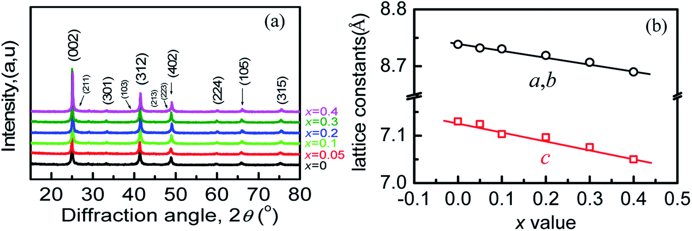 | ||
| Fig. 1 (a) X-ray diffraction patterns of the Cu3+xIn5−xGaxTe9 powders; (b) lattice constants a, b and c as a function of x value, which follows the Vegard's law. | ||
3.2 Microstructure analyses
In order to further confirm the synthesis of titled alloys, the microstructures of the samples at x = 0 (Vc = 0.11) and 0.3 (Vc = 0.078) have been examined by using high-resolution TEM (HRTEM). Fig. S3a† is the TEM image of the powder sample (x = 0), and Fig. S3b† is the corresponding HRTEM image. Fig. S3c† is the corresponding selected area electron diffraction (SAED) pattern, and Fig. S3d† showing zoomed view of Fig. S3b,† in which the d spacing between (002) crystal planes is about 0.364 nm. This value is a little larger than 0.357 nm indicated in PDF51-0804. Fig. S4a and b† are the TEM and HRTEM images for the sample at x = 0.3. Fig. S4c† is the corresponding SAED pattern, and Fig. S4d† is an enlarged image. The d spacing between (002) crystal planes is ∼0.33 nm, about 0.027 nm less. The decreasing tendency in d spacing is caused by the smaller atomic Ga than In, in a good agreement with the analyzed XRD data (Fig. 1b).3.3 Band structures
In order to have a better understanding of the changes of the transport properties upon Ga substitution in Cu3In5Te9, we calculate the band structures of Cu10In17Te32 (Fig. S5a†) and Cu11In16GaTe32 with an extra Cu addition and Ga residing at the In site (Fig. S5b†). It is observed the conduction band (CB) moves down upon an incorporation of Ga (Fig. 2a and b), while the valence band maximum (VBM) remains the same energy level (Fig. 2b and c), which narrows the bandgap (Eg) from ∼1.0 eV to 0.7 eV. According to the Goldsmid estimation Eg = 2e|α|maxTmax,38 the Eg value decreases from 0.64 eV to 0.43 eV as x value increases from 0 to 0.3. Here, the |α|max represents the highest Seebeck coefficients (see below), Tmax temperature at which the highest Seebeck coefficients present, and e electronic charge. Although the estimated Eg values are somewhat inaccurate, they are only a little lower than nκBT (n = 6–10) (0.42–0.68 eV to 0.52–0.87 eV) for the best direct-gap TE materials.39 This implies that the Goldsmid's equation is still useful to estimate the bandgap, in terms of the Gibbs's suggestion.40 Besides, the incorporation of Ga flattens the conduction band (CB) and brings valence band (VB) at Z, R and G points closer in energy (Fig. 2b), thus resulting in CB and VB convergences (Fig. 2a and b). Although the contribution of the orbital Ga in both the VBM and CBM seems to be limited (Fig. 2d), it might play a significant role in promoting the down-movement of CB, in addition to the flattening of CB. Such changes in band structure would evidently enhance the carrier concentration.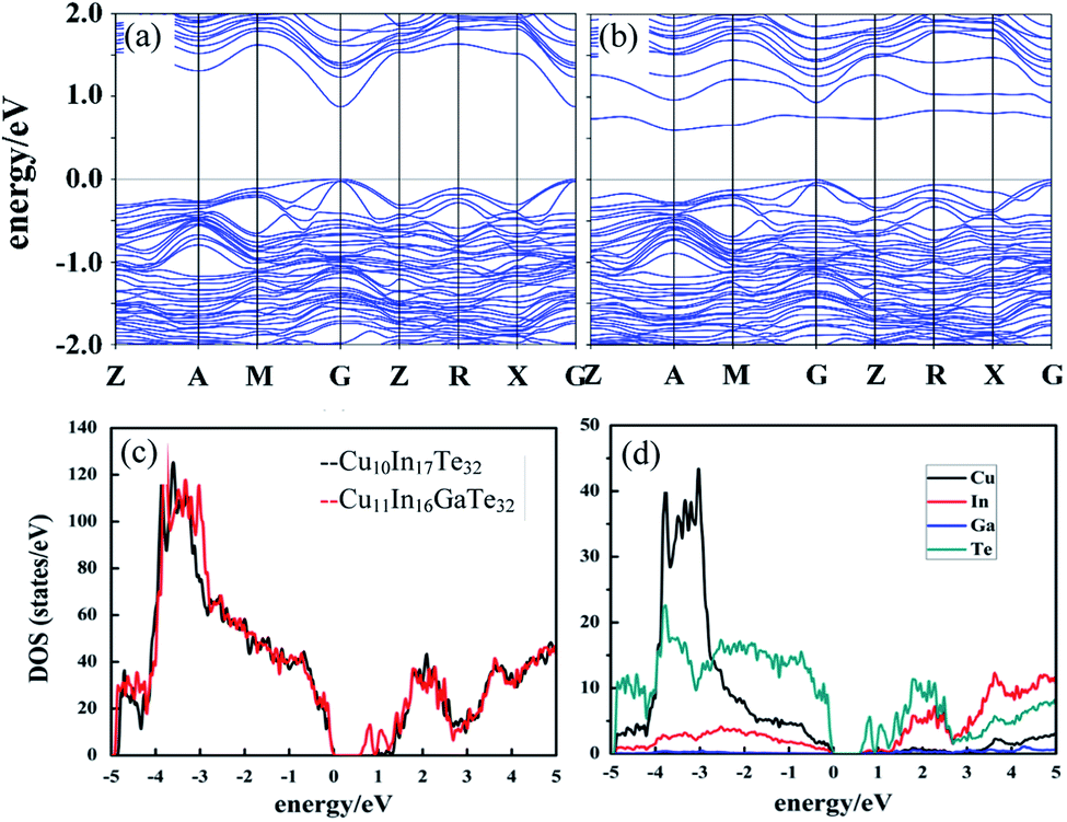 | ||
| Fig. 2 Electronic band structures of (a) Cu10In17Te32 and (b) Cu11In16GaTe32; (c) density of the states (DOS) for Cu10In17Te32 and Cu11In16GaTe32; (d) projected densities of the states (PDOS) for Cu11In16GaTe32. The highest occupied state is set as the zero energy value. It was observed that the conduction bands move down upon substitution of Ga for In, which narrows the bandgap. | ||
3.4 Transport and TE performance
To evidence the above assumption, we have measured the Hall coefficients at RT and then obtained the Hall carrier concentrations (nH) and mobility. The measurements show that the nH value increases from 1.96 × 1018 cm−3 (x = 0) to ∼1.0 × 1019 cm−3 (x = 0.3) before it starts to fall, albeit very slightly, to 9.44 × 1018 cm−3 (x = 0.4), while the Hall mobility (μ) increases from 25.0 cm2 V−1 s−1 (x = 0) to 33.9 cm2 V−1 s−1 (x = 0.1), and then decreases to 13.2 cm2 V−1 s−1 at x = 0.4, as shown in Fig. 3. The general enhancement in nH is due to the bandgap narrowing, while the reduction in mobility μ is mainly ascribed to the increased carrier scattering. As the x value increases the copper vacancy Vc decreases. This implies that the presence of the high copper vacancy is not beneficial to the carrier concentration.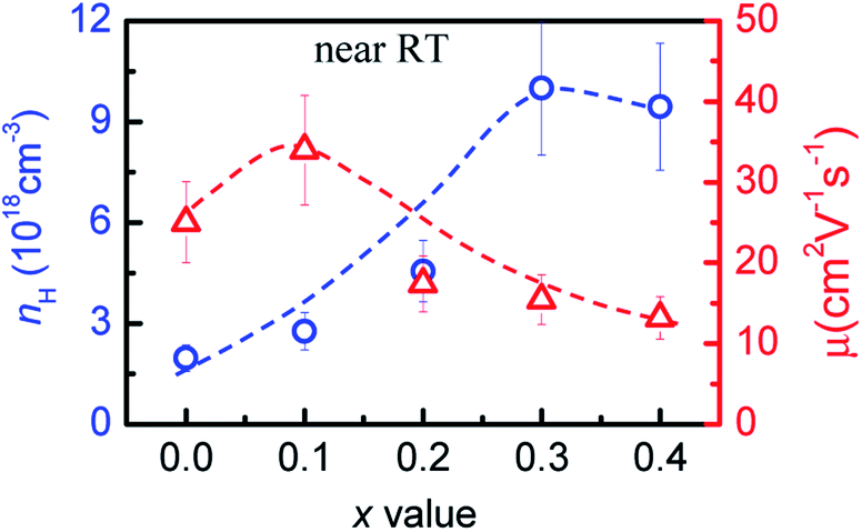 | ||
| Fig. 3 Hall carrier concentration (nH) and mobility (μ) as a function of x value in Cu3+xIn5−xGaxTe9. | ||
The thermoelectric performance is presented in Fig. 4, where the Seebeck coefficients (α) are shown as a function of temperature in Fig. 4a. The positive α values indicate the p-type semiconductor behavior of the materials. With the x (Vc) value increasing (decreasing), the highest α value decreases from 315.9 μV K−1 (x = 0, Vc = 0.11) to 268.2 μV K−1 (x = 0.3, Vc = 0.078), and so does the temperature at which the highest α value appears, guided by a gray arrow in Fig. 4a. This implies that the bandgap narrows as x (Vc) value increases (decreases), which is in accordance with the first-principles calculation. However, the α values at x = 0.4 (Vc = 0.067) are higher than those at x = 0.3 (Vc = 0.078), which might be the low carrier concentration at x = 0.4 (Vc = 0.067).
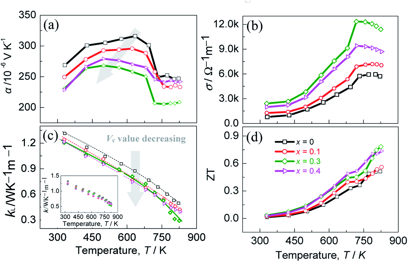 | ||
| Fig. 4 Thermoelectric performance of the materials as a function of temperature for different x values. (a) Seebeck coefficients (α) as a function of temperature; (b) electrical conductivity (σ) as a function of temperature; (c) lattice thermal conductivity (κL) as a function of temperature, the inset is the total κ; (d) dimensionless figure of merit (ZT) as a function of temperature. | ||
Besides, above ∼700 K the Seebeck coefficients of all the samples decrease rapidly with temperature increasing, and then keep a relatively stable value above ∼730 K. Such a change is most likely to be related to the order-disorder transition near 700 K (Fig. S6†).41–43 The combined TGA/DSC analyses of the material from ambient temperature to ∼850 K reveal an exothermic effect around 700 K, which confirms this issue. Unfortunately, this transition has not been reported in detail previously.14,44,45 Besides, there is little or no indication of element Te evaporation below ∼740 K from the DSC curve. Only when the temperature rises to above ∼740 K does the weight loss of the sample occur. Therefore, the scattered data of the TE properties above 740 K might be ascribed to the deprivation of gravity.
Fig. 4b is the temperature-dependent electrical conductivities (σ), which increase with temperature until at ∼730 K. Above ∼730 K, the materials exhibit metallic-like behavior, as was observed in AgGa1−xTe2 system.46 Besides, it is noted that the electrical conductivity at ∼822 K increases from 5.7 × 10³ Ω−1 m−1 (x = 0, Vc = 0.11) to 11.4 × 10³ Ω−1 m−1 (x = 0.3, Vc = 0.078) before it starts to fall to the 8.7 × 10³ Ω−1 m−1 (x = 0.4, Vc = 0.067), which corresponds to the variations in carrier concentration and mobility (Fig. 3). The lattice thermal conductivities (κL) are displayed as a function of temperature in Fig. 4c, where the inset is the total κ. Roughly, the lattice parts (κL) bear resemblance to total κ, which suggests that the phonon transport plays a major role in heat carrying. With the x(Vc) value increasing (decreasing), the lattice part (κL) reduces generally. However, above ∼780 K the κL(κ) at x = 0.3 (Vc = 0.078) reduce relatively rapidly, and at ∼822 K they reach the lowest values, 0.30 Wm−1 K−1 and 0.52 Wm−1 K−1. The rapid reduction in κL at high temperatures is likely attributed to the enhanced point defect scattering of phonons resulting from the combined effects of GaIn and copper vacancy. However, the high κL values (x = 0.4, Vc = 0.067) at high temperatures might be due to the fact that the weakened scattering of phonons at copper vacancies neutralizes to some extent the scattering on the defect GaIn. It is therefore concluded that a co-regulation of copper vacancy concentration (Vc) and the extra point defects is essential to minimize the lattice component κL.
Combined with the above transport properties, the highest ZT value of ∼0.8 is attained at x = 0.3 (Vc = 0.078), as shown in Fig. 4d. Although this ZT value is not high compared with those of the state-of-the-art TE materials, such as PbTe-,47 SnSe-,48 CuGa(In)Te2-based TE compounds,1,49 it has ∼60% enhancement compared to the pristine Cu3In5Te9 (x = 0, Vc = 0.11). This emphasizes the importance again of co-regulation of the copper vacancy concentration and point defects in Cu3In5Te9-based chalcogenides.
In order to further elucidate the highest TE performance of the material with Vc = 0.078, we, specifically, present the relationship between the copper vacancy concentration (Vc) and lattice thermal conductivity (κL). The result is shown in Fig. 5, where we have observed that the lattice parts (κL) at ∼RT, ∼693 K and ∼822 K tend to increase as the Vc value increases. The solid lines in Fig. 5 are indicated as a guidance for eye. Although the lattice parts (κL) in the present chalcogenides are related to the combined scatterings, that is, phonon scatterings at point defects of copper vacancy and GaIn, the above dependences at least indicate that the cation vacancy concentration does not play a predominant role in scattering phonons. Only when the material has a proper Vc value (Vc = 0.078) combined with an extra point defect GaIn, are the electrical and thermal properties co-optimized. This finding does not support the common understanding that the presence of cation vacancy in ternary chalcogenides has a definitely positive effect on either the carrier concentration5 or phonon scattering.17,23
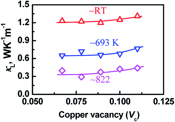 | ||
| Fig. 5 Lattice thermal conductivities at ∼RT, ∼693 K and ∼822 K as a function of copper vacancy concentration (Vc). | ||
4. Conclusions
In summary, the Cu3In5Te9-based chalcogenides with a substitution of Ga for In and an addition of extra Cu were prepared and their TE performance were investigated. The results reveal that the co-regulation of the copper vacancy concentration (Vc) and phonon scattering are vital to improve the TE performance. The optimal Vc is 0.078 in these compounds at which the highest TE figure of merit ZT of ∼0.8 is attained at ∼822 K, which is ∼60% higher than that of pristine Cu3In5Te9. This indicates that the co-regulation of the copper vacancy and phonon scattering might be a good way to explore the high performance TE chalcogenides.Conflicts of interest
There are no conflicts of interest to declare.Acknowledgements
This work is supported by the National Natural Science Foundation of China (51671109, 51171084).Notes and references
- Y. Luo, J. Yang, Q. Jiang, W. Li, D. Zhang, Z. Zhou, Y. Cheng, Y. Ren and X. He, Adv. Energy Mater., 2016, 6, 1600007 CrossRef.
- F. Fan, L. Wu and S. Yu, Energy Environ. Sci., 2014, 7, 190 RSC.
- A. Kosuga, K. Umekage, M. Matsuzawa, Y. Sakamoto and I. Yamada, Inorg. Chem., 2014, 53, 6844 CrossRef CAS.
- J. Shen, X. Zhang, S. Lin, J. Li, Z. Chen, W. Li and Y. Pei, J. Mater. Chem. A, 2016, 4, 15464 RSC.
- A. Yusufu, K. Kurosaki, A. Kosuga, T. Sugahara, Y. Ohishi, H. Muta and S. Yamanaka, Appl. Phys. Lett., 2011, 99, 061902 CrossRef.
- Z. Xia, G. Wang, X. Zhou and W. Wen, Ceram. Int., 2017, 43, 16276 CrossRef CAS.
- R. Liu, Y. Qin, N. Cheng, J. Zhang, X. Shi, Y. Grin and L. Chen, Inorg. Chem. Front., 2016, 3, 1167 RSC.
- G. E. Delgado, C. Rincón and G. Marroquín, Rev. Mex. Fis., 2019, 65, 360 CrossRef.
- M. Parlak, Ç. Erçelebi, İ. Günal, H. Özkan, N. M. Gasanly and A. Çulfaz, Cryst. Res. Technol., 1997, 32, 395 CrossRef CAS.
- C. C. Rincón, S. M. Wasim, G. Marín, J. M. Delgado and J. Contreras, Appl. Phys. Lett., 2003, 83, 1328 CrossRef.
- T. Ren, P. Ying, G. Cai, X. Li, Z. Han, L. Min and J. Cui, RSC Adv., 2018, 8, 27163 RSC.
- M. Li, Y. Luo, G. Cai, X. Li, X. Li, Z. Han, X. Lin, D. Sarker and J. Cui, J. Mater. Chem. A, 2019, 7, 2360 RSC.
- T. Ren, Z. Han, P. Ying, X. Li, X. Li, X. Lin, D. Sarker and J. Cui, ACS Appl. Mater. Interfaces, 2019, 11, 32192 CrossRef CAS.
- E. Guedeza, L. Mogollónb, G. Marcanoa, S. M. Wasima, G. Sánchez Péreza and C. Rincón, Mater. Lett., 2017, 186, 155 CrossRef.
- G. J. Snyder and E. S. Toberer, Nat. Mater., 2008, 7, 105 CrossRef CAS.
- Y. Luo, Q. Jiang, J. Yang, W. Li, D. Zhang, Z. Zhou, Y. Cheng, Y. Ren, X. He and X. Li, Nano Energy, 2017, 32, 80 CrossRef CAS.
- T. Plirdpring, K. Kurosaki, A. Kosuga, M. Ishimaru, A. Harnwunggmoung, T. Sugahara, Y. Ohishi, H. Muta and S. Yamanaka, Mater. Trans., 2012, 53, 1212 CrossRef CAS.
- K. Kurosaki and S. Yamanaka, Phys. Status Solidi A, 2013, 210, 82 CrossRef CAS.
- A. Klein and W. Jaegermann, Appl. Phys. Lett., 1999, 74, 2283 CrossRef CAS.
- S. M. Wasim, C. Rincón, G. Marín and J. M. Delgado, Appl. Phys. Lett., 2000, 77, 94 CrossRef CAS.
- Y. Fujii, K. Tanaka and A. Kosuga, Scr. Mater., 2019, 162, 272 CrossRef CAS.
- K. Wang, P. Qin, Z. Ge and J. Feng, Scr. Mater., 2018, 149, 88 CrossRef CAS.
- Z. Ye, J. Cho, M. M. Tessema, J. R. Salvador, R. A. Waldo, H. Wang and W. Cai, J. Solid State Chem., 2013, 201, 262 CrossRef CAS.
- S. Wei, S. B. Zhang and A. Zunger, Appl. Phys. Lett., 1998, 72, 3199 CrossRef CAS.
- Y. Qin, P. Qiu, R. Liu, Y. Li, F. Hao, T. Zhang, D. Ren, X. Shi and L. Chen, J. Mater. Chem. A, 2016, 4, 1277 RSC.
- J. Cui, G. Cai and W. Ren, RSC Adv., 2018, 8, 21637 RSC.
- J. Yang, S. Chen, Z. Du, X. Liu and J. Cui, Dalton Trans., 2014, 43, 15228 RSC.
- W. D. Carr and D. T. Morelli, J. Alloys Compd., 2015, 630, 277 CrossRef CAS.
- R. Guevara, G. Marín, J. M. Delgado, S. M. Wasim, C. Rincón and G. Sánchez Pérez, J. Alloys Compd., 2005, 393, 100 CrossRef CAS.
- A. Kosuga, T. Plirdpring, R. Higashine, M. Matsuzawa, K. Kurosaki and S. Yamanaka, Appl. Phys. Lett., 2012, 100, 042108 CrossRef.
- H. Kim, Z. M. Gibbs, Y. Tang, H. Wang and G. J. Snyder, APL Mater., 2015, 3, 041506 CrossRef.
- T. Degen, M. Sadki, E. Bron, U. König and G. Nénert, Powder Diffr., 2014, 29, S13–S18 CrossRef CAS.
- V. Blum, R. Gehrke, F. Hanke, P. Havu, V. Havu, X. Ren, K. Reuter and M. Scheffler, Comput. Phys. Commun., 2009, 180, 2175 CrossRef CAS.
- P. Hohenberg and W. Kohn, Phys. Rev., 1964, 136, B864 CrossRef.
- W. Kohn and L. J. Sham, Phys. Rev., 1965, 140, A1133 CrossRef.
- J. P. Perdew, K. Burke and M. Ernzerhof, Phys. Rev. Lett., 1996, 77, 3865 CrossRef CAS.
- A. V. Krukau, O. A. Vydrov, A. F. Izmaylov and G. E. Scuseria, J. Chem. Phys., 2006, 125, 224106 CrossRef.
- H. J. Goldsmid and J. W. Sharp, J. Electron. Mater., 1999, 28, 869 CrossRef CAS.
- J. O. Sofo and G. D. Mahan, Phys. Rev. B: Condens. Matter Mater. Phys., 1994, 49, 4565 CrossRef CAS.
- Z. M. Gibbs, H. Kim, H. Wang and G. J. Snyder, Appl. Phys. Lett., 2015, 106, 022112 CrossRef.
- A. Zunger, Appl. Phys. Lett., 1987, 50, 164 CrossRef CAS.
- S. Schorr, G. Geandier and B. V. Korzun, Phys. Status Solidi C, 2006, 3, 2610 CrossRef CAS.
- C. Rincón, Solid State Commun., 1987, 64, 663 CrossRef.
- H. Özkan, N. Gasanly, İ. Yilmaz, A. Çulfaz and V. Naglev, Turk. J. Phys., 1998, 22, 519 Search PubMed.
- N. M. Gasaanly, A. G. Guseinov, E. A. Aslanov and S. A. EL-Hamid, Phys. Status Solidi B, 1990, 158, K85 CrossRef.
- X. Su, N. Zhao, S. Hao, C. C. Stoumpos, M. Liu, H. Chen, H. Xie, Q. Zhang, C. Wolverton, X. Tang and M. G. Kanatzidis, Adv. Funct. Mater., 2018, 29, 1806534 CrossRef.
- J. Zhang, D. Wu, D. He, D. Feng, M. Yin, X. Qin and J. He, Adv. Mater., 2017, 29, 1703148 CrossRef.
- L. Zhao, G. Tan, S. Hao, J. He, Y. Pei, H. Chi, H. Wang, S. Gong, H. Xu, V. P. Dravid, C. Uher, G. J. Snyder, C. Wolverton and M. G. Kanatzidis, Science, 2016, 351, 141 CrossRef CAS.
- T. Plirdpring, K. Kurosaki, A. Kosuga, T. Day, S. Firdosy, V. Ravi, G. J. Snyder, A. Arnwunggmoung, T. Sugahara, Y. Ohishi, H. Muta and S. Yamanaka, Adv. Mater., 2012, 24, 3622 CrossRef CAS.
Footnote |
| † Electronic supplementary information (ESI) available. See DOI: 10.1039/c9ra06565b |
| This journal is © The Royal Society of Chemistry 2019 |