
 Open Access Article
 This Open Access Article is licensed under a Creative Commons Attribution-Non Commercial 3.0 Unported Licence
The photoluminescence, field emission and femtosecond nonlinear absorption properties of Al-doped ZnO nanowires, nanobelts, and nanoplane-cone morphologies
Yu-Tong Cao,
Yu Cai,
Cheng-Bao Yao *,
Sheng-Bin Bao and
Yue Han
*,
Sheng-Bin Bao and
Yue Han
Key Laboratory of Photonic and Electric Bandgap Materials, Ministry of Education, School of Physics and Electronic Engineering, Harbin Normal University, Harbin, 150025, Heilongjiang Province, China. E-mail: yaochengbao5@163.com
First published on 29th October 2019
Abstract
Al-doped ZnO (AZO) nanowires, nanobelts and nanoplane-cone nanostructures have been successfully synthesized. The structural, photoluminescence (PL) and field emission (FE) properties of AZO nanowires have been characterized. The dependence of the PL properties of AZO nanostructures versus excitation laser power in the range from 1 to 12 mW and temperature in the range of 10–273 K was discussed. The PL measurement results demonstrated that the ultraviolet emission came from a near band edge emission, and two peaks in visible light region were due to deep-level emission. Moreover, the AZO nanowires have a relatively stronger ultraviolet emission than other kinds of samples. The FE measurements indicate that the turn-on field for the nanoplane-cone structure is 2.52 V μm−1, which is smaller than 4.42 V μm−1 for nanowires and 5.28 V μm−1 for nanobelts. In addition, the nonlinear absorption properties of AZO nanowires were measured using a femtosecond Z-scan technique. The effect of morphology on the nonlinear optical absorption properties of AZO nanowires was studied. From the results, the AZO nanowires show reverse saturable absorption (RSA) behavior. Furthermore, the results show that the order of magnitude of the nonlinear absorption coefficient for AZO nanowires is ∼10−2 cm3 GW−2. Our results show that AZO films are a promising candidate in further optoelectronic device applications.
1. Introduction
1D pure zinc oxide (ZnO) and metal-doped ZnO nanostructures are considered to have potential applications in electronics, and photon and sensor components due to their excellent optical and electrical properties.1–8 Also the metal doping amount controls the optical band gap of ZnO. Particularly, in earlier reports,9,10 Ga, Al and In metal doped ZnO materials have received considerable attention due to their interesting photoelectric and nonlinear optical properties. Al is an excellent dopant for ZnO due to it having a single positive Al3+, and the Al3+ has a smaller ionic radius than Zn2+.11 Al is preferable as a dopant source; it is more suitable to occupy the interstitial site. In addition, due to the doping of aluminum, the resistivity of the zinc oxide nanostructure, the high transmittance in the visible light region and the thermal stability are improved. To date, some researchers have studied a variety of Al doped ZnO (AZO) nanostructures, among which thin films,12–14 nanofibers,15 micron rods,16 nanowires,17,18 nanorods19 and nanoparticles20,21 have been successfully prepared by various methods. For AZO thin films, F. Khan et al.12 have reported influence of excitation wavelength on PL spectra of AZO films. M. Chen et al.13 have reported surface characterization of transparent conductive oxide AZO films. M. Shirazi et al.14 have reported PL of AZO film by spray pyrolysis method. The results show that the near band edge (NBE) emission in PL spectra shifts to shorter wavelengths and Fermi surface shifts to conduction band with increasing the Al content. Y. Liu et al.15 found a decrease in green emission intensity of AZO nanofibers with increasing the Al concentration. Compared with other dopants ZnO nanomaterials, AZO nanostructures have been presented for the high conductance duo to provided more electrons, which can be expected to have a green emission band, a low turn-on electric field (EF) and a high emission current (EC).20 J. L. Wang et al.21 have reported FE characteristics of AZO nanowires at different oxygen annealing temperature. AZO film has been reported by many researchers. Hence, it is important to investigate the influence of the dopants on the structural, morphologies and properties of ZnO nanostructure.22,23 However, the morphologies of 1D AZO nanomaterial are seldom reported. The influence of morphology on the structural, photoelectric and ultrafast nonlinear optical behavior properties of AZO nanomaterials is still lacking.In this work, AZO nanostructures with nanowires, nanobelts and nanoplane-cone morphologies had been successfully synthesized. We study the effect of different parameters on the morphologies and nanostructures. The results show that different experimental parameters lead to different sample morphologies. The room and low temperature photoluminescence (RTPL/LTPL) spectra and FE properties of the AZO nanostructures were further investigated. The results show that different morphologies and components affect the location and intensity of the emission peak. The resulting FE showed that the superior FE properties are attributed to the better morphologies. Ultrafast nonlinear optical studies in semiconductor materials have proven extremely powerful in understanding photoelectric properties of materials that are crucially important in optical devices applications.
2. Experiment
The powder mixture of ZnO and Al as evaporation source was placed into a ceramic boat and loaded into the tubular furnace. And the Si (100) substrates with Au films were placed downstream from the powders. Detailed experimental conditions (the preset temperature (T/°C), quality ratio of ZnO![[thin space (1/6-em)]](https://www.rsc.org/images/entities/char_2009.gif) :Al, flow rate of carrier gas (V/sccm), the evaporation time (t/min), distance between substrate and evaporation source (L/cm)) are listed in Table 1. Two important factors are responsible for the growth of AZO nanostructures: the formation of crystalline nuclei and axial growth of AZO nuclei. The formation of nuclei depends on experimental conditions parameters. When the temperature exceeds 1250 °C, ZnO is easily separated into Zn2+ and O2−, and Al is easily separated into Al3+. Owing to the fast converge of all ions in low temperature range, nanosized crystal nuclei were generated. In addition, since ZnO is a polar crystal, where zinc and oxygen atoms are arranged alternatively along the c-axis and the top/bottom surface of Zn with catalytically active and oxygen with chemically inert terminated, respectively. With the control of gas velocity and distance, various morphologies of AZO nanostructures were formed. Moreover, since Al atoms have lower vapor pressure than Zn atoms, the characteristic diameter would be increased with increasing Al composition. Simply it is directly related to the number of deposited particles. Growth mechanism of 1D-AZO nanostructures was shown in Scheme 1. In the Scheme 1(a), AZO nanowires are up to several tens of microns in length and have a catalyst particle at the tip. In Scheme 1(c), the AZO nanobelts were grown by increasing ZnO vapor concentration which prompted the growth of nanobelts. However, further increase of doping prompted the growth of nanoplane-cone, due to the difference of radius between Zn2+ ion (0.074 nm) and Al3+ ion (0.053 nm), which changes the interplanar crystal spacing, and results in a measurable lower angle shift of the (100) and (101) peaks, as shown in Scheme 1(d). But Al can be incorporated in ZnO system either as a substituent for Zn2+ and suppress the growth of ZnO. X-ray diffraction (XRD), field emission scanning electron microscope (SEM), energy dispersive spectroscopy (EDS), transmission electron microscopy (TEM), high resolution transmission electron microscopy (HRTEM), selected area electron diffraction (SAED), field emission auger electron spectrometers (FEAES), RTPL and LTPL characterization for samples were performed, respectively. The Z-scan experiments are performed using a Q-switched, frequency doubled Ti:sapphire laser producing 150 fs laser pulses with a pulse repetition rate of 1 kHz at wavelength of 800 nm. Basically, in this technique the nonlinear sample is scanned through the focal plane of a tightly focused Gaussian beam. Unstability of the Gaussian beam intensity is ±0.2%. These methods are described in detail in previous reports.24
:Al, flow rate of carrier gas (V/sccm), the evaporation time (t/min), distance between substrate and evaporation source (L/cm)) are listed in Table 1. Two important factors are responsible for the growth of AZO nanostructures: the formation of crystalline nuclei and axial growth of AZO nuclei. The formation of nuclei depends on experimental conditions parameters. When the temperature exceeds 1250 °C, ZnO is easily separated into Zn2+ and O2−, and Al is easily separated into Al3+. Owing to the fast converge of all ions in low temperature range, nanosized crystal nuclei were generated. In addition, since ZnO is a polar crystal, where zinc and oxygen atoms are arranged alternatively along the c-axis and the top/bottom surface of Zn with catalytically active and oxygen with chemically inert terminated, respectively. With the control of gas velocity and distance, various morphologies of AZO nanostructures were formed. Moreover, since Al atoms have lower vapor pressure than Zn atoms, the characteristic diameter would be increased with increasing Al composition. Simply it is directly related to the number of deposited particles. Growth mechanism of 1D-AZO nanostructures was shown in Scheme 1. In the Scheme 1(a), AZO nanowires are up to several tens of microns in length and have a catalyst particle at the tip. In Scheme 1(c), the AZO nanobelts were grown by increasing ZnO vapor concentration which prompted the growth of nanobelts. However, further increase of doping prompted the growth of nanoplane-cone, due to the difference of radius between Zn2+ ion (0.074 nm) and Al3+ ion (0.053 nm), which changes the interplanar crystal spacing, and results in a measurable lower angle shift of the (100) and (101) peaks, as shown in Scheme 1(d). But Al can be incorporated in ZnO system either as a substituent for Zn2+ and suppress the growth of ZnO. X-ray diffraction (XRD), field emission scanning electron microscope (SEM), energy dispersive spectroscopy (EDS), transmission electron microscopy (TEM), high resolution transmission electron microscopy (HRTEM), selected area electron diffraction (SAED), field emission auger electron spectrometers (FEAES), RTPL and LTPL characterization for samples were performed, respectively. The Z-scan experiments are performed using a Q-switched, frequency doubled Ti:sapphire laser producing 150 fs laser pulses with a pulse repetition rate of 1 kHz at wavelength of 800 nm. Basically, in this technique the nonlinear sample is scanned through the focal plane of a tightly focused Gaussian beam. Unstability of the Gaussian beam intensity is ±0.2%. These methods are described in detail in previous reports.24
| Sample | Quality ratio of ZnO:Al |
V (sccm) | T (°C) | t (min) | L (cm) |
|---|---|---|---|---|---|
| Nanowires | 5:1 |
20 | 1250 | 30 | 21.4 |
| Nanobelts | 4:1 |
60 | 1250 | 30 | 16.2 |
| Nanoplane-cone | 4:1 |
100 | 1250 | 30 | 17.0 |
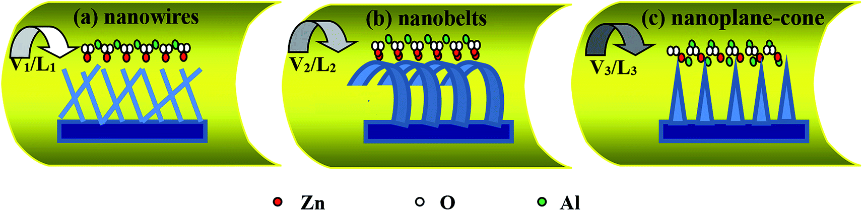 | ||
| Scheme 1 A schematic illustration of growth mechanism for AZO nanostructures. V1–3, L1–3 shows the flow rate of carrier gas and distance between substrate and evaporation source for three samples; (a) nanowires, (b) nanobelts and (c) nanoplane-cones. | ||
3. Results and discussion
Fig. 1 shows the XRD pattern of the AZO nanostructures with nanowires, nanobelts and nanoplane-cone morphologies. The diffraction peaks at 2θ (degrees) of 36.446 are indexed planes of Al. The other diffraction peaks at 2θ (degrees) are indexed planes of ZnO (JCPDS card no. 76-704). And the lattice constant of AZO nanostructures was smaller than that of the pure ZnO (a = 0.32475–0.32501 nm, c = 0.52042–0.52075 nm (ref. 26)). Since the ionic radius of Al3+ (0.053 nm) is smaller than the ionic radius of Zn2+ (0.074 nm), the Al atom replaces the Zn atom at the lattice position, resulting in a decrease in lattice constant. In addition, as can be seen from Fig. 1 the (0002) crystalline plane distance decreases, and the diffraction angle increases. So the lattice constant c of AZO nanostructure is smaller than that of the bulk ZnO, all the nanostructures exhibit residual tensile strain.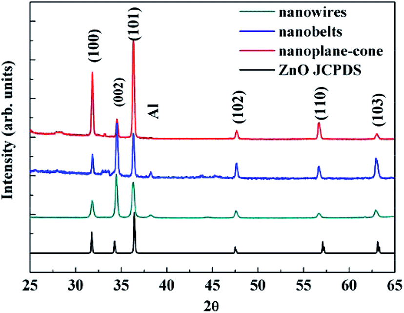 | ||
| Fig. 1 X-ray diffraction spectrum of AZO nanostructures. | ||
Fig. 2 (M1, M2 and M3, M = a, b, c) shows a low magnification, high magnification and the cross section thickness of SEM image of all samples. The results showed AZO nanostructures with nanowires, nanobelts and nanoplane-cone morphologies have been successfully synthesized. The insets of Fig. 2 (M3) are magnified SEM image with cross section of such structures. The image shows evidence of the nanostructured morphology of the AZO. It is obvious that the morphology of AZO has quite differences, namely nanowires (V/d = 0.93), nanobelts (V/d = 3.7), and nanoplane-cone (V/d = 5.9). Fig. 2(a) exhibits thickness uniform three-edged 1D nanowires, which has a diameter of around 84 nm and a total length of several microns (not shown). Fig. 2(b) exhibits hexagonal nanobelts at 312 nm width and 92 nm thicknesses. Fig. 2(c) exhibits nanoplane-cone with wide (thick) end and narrow (tip) end. From the results, the diameter of single AZO nanoplane-cone is around 600 nm and 20 nm (for wide (thick) and narrow (tip) parts of nanoplane-cone), respectively. Fig. 3 shows the typical composition analysis of the AZO nanostructures. EDS demonstrate only Zn, O and Al element. And no peaks are detected from other element materials. In addition, with the increase of distance between substrate and evaporation source, the concentration of incorporated Al increased (in Fig. 3, at% of Al for nanowire > nanoplane-cone > nanobelts).
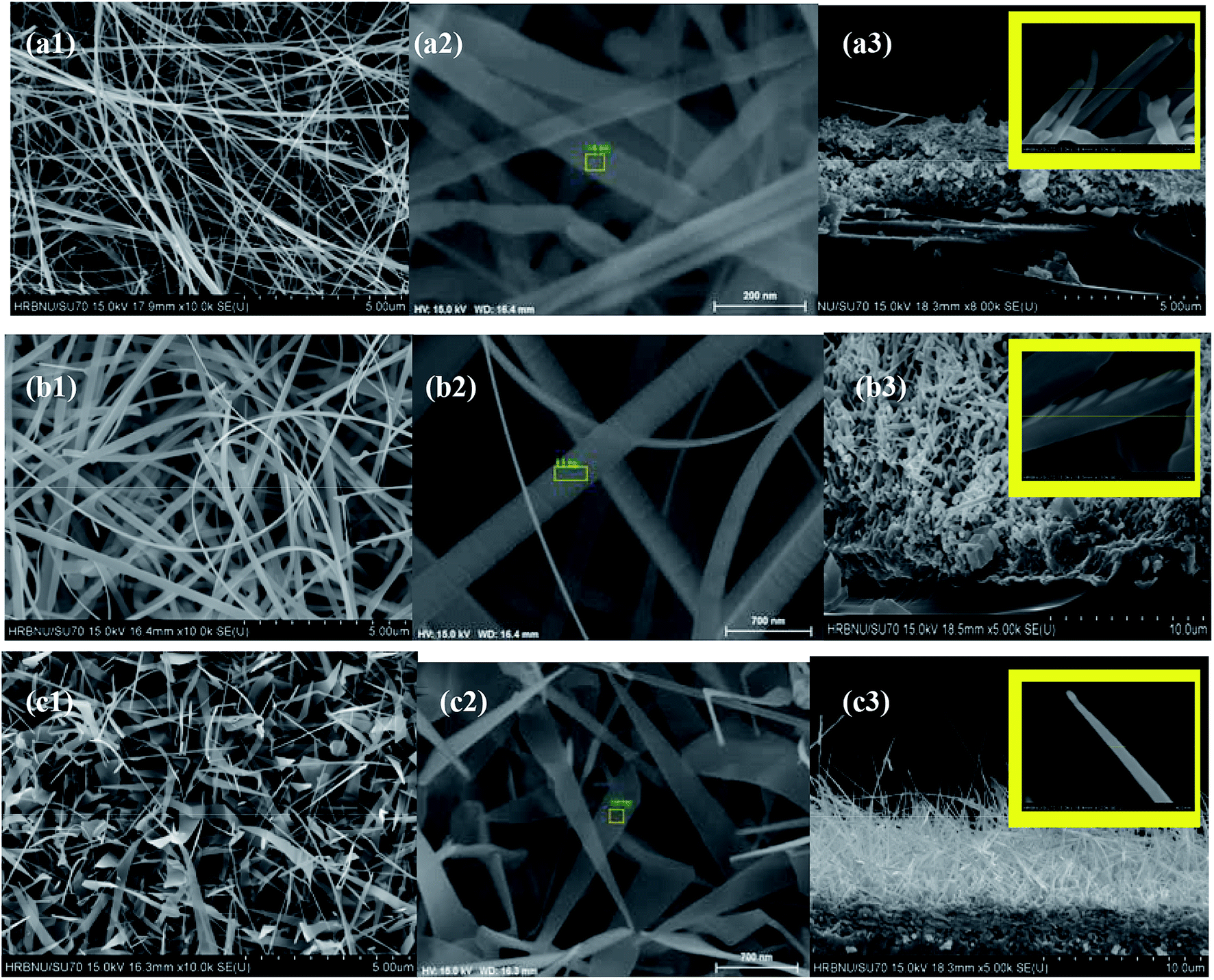 | ||
| Fig. 2 Schematic SEM diagrams of AZO nanostructures with different morphologies: (a) nanowires, (b) nanobelts, and (c) nanoplane-cone. | ||
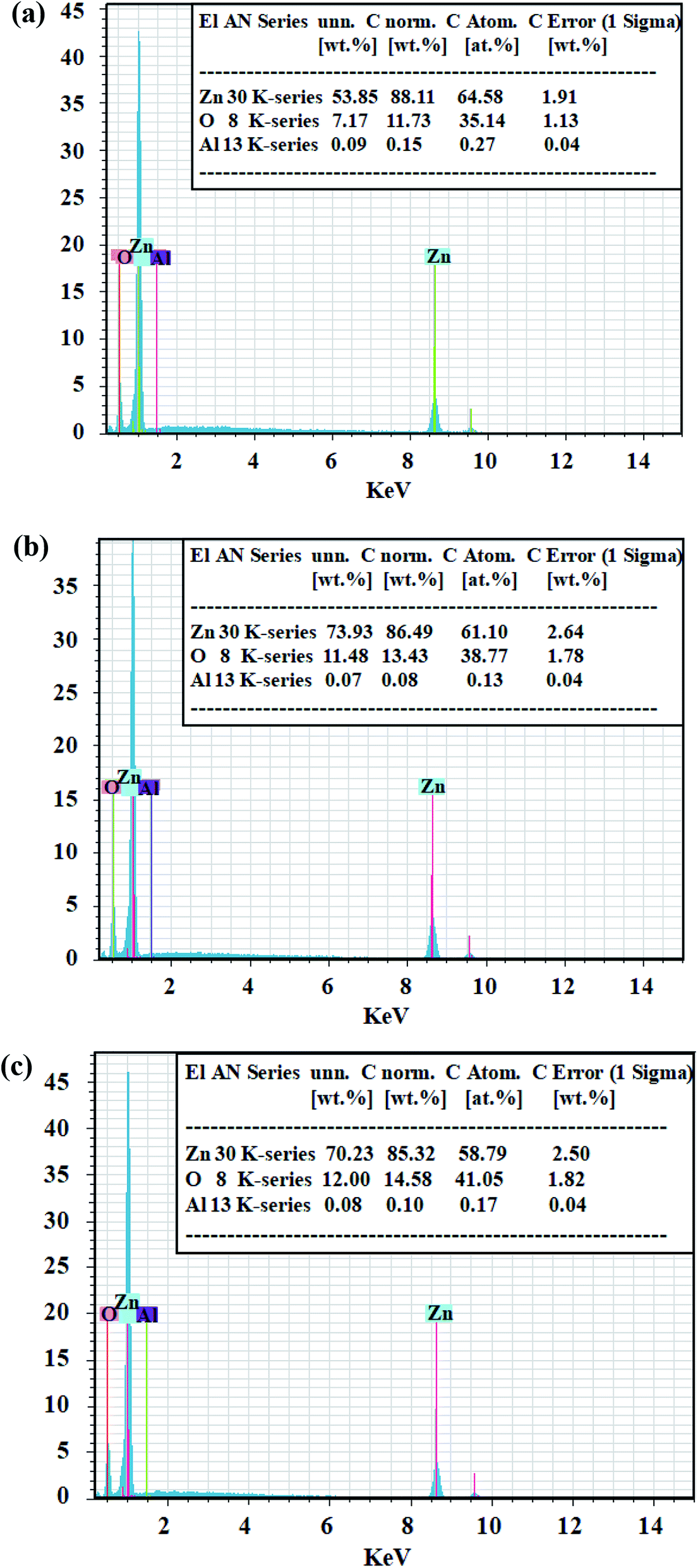 | ||
| Fig. 3 Schematic EDS diagrams of AZO nanostructures with different morphologies: (a) nanowires, (b) nanobelts, and (c) nanoplane-cone. | ||
Fig. 4 (M1) shows the TEM characterization of all samples. The Fig. 4 (M2) and (M3) are HRTEM image and SAED pattern, respectively. The diameter of single AZO nanostructures is around 84 nm (for nanowires), 312 nm (for nanobelts), 20 nm and 600 nm (for narrow (tip) and wide (thick) parts of nanoplane-cone), respectively. The SAED pattern in Fig. 4 (M3) shows that the AZO nanostructures are single crystalline in nature and grow along the [0001] direction. The XRD and FESEM results are in agreement with the TEM analysis.
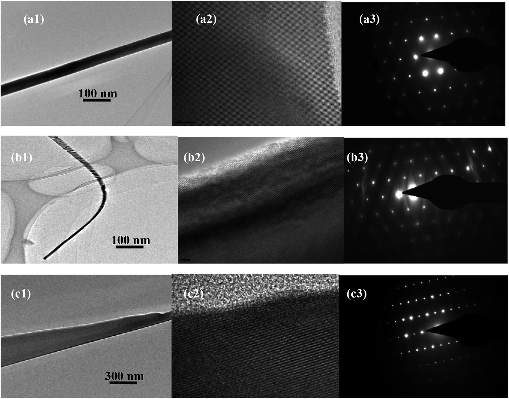 | ||
| Fig. 4 TEM, high resolution TEM and selected area electron diffraction diagrams of different AZO nanostructures: (a) nanowires, (b) nanobelts, and (c) nanoplane-cone, respectively. | ||
In order to study the chemical state of Zn, Al and O, we measured the XPS spectrum of the sample, as is shown in Fig. 5. The binding energies obtained in the XPS analysis were standardized by using C 1s at 284.6 eV as the reference. Fig. 5(a) shows the XPS survey spectrum of the AZO nanowires. No peaks of other elements except Zn, O and Al are observed in the spectrum. Fig. 5(b) and (c) shows the XPS spectra of the O 1s and Zn 2p3/2 regions for the surface of the AZO nanowires. The O 1s core-level peak at 532.4 eV indicates the −2 valence of the O element in the products. The peaks located at 1022.1 and 1045.2 eV correspond to Zn 2p3/2 and Zn 2p1/2, respectively (see Fig. 5(c)). From the Fig. 5(d), the core-level spectrum of Al 2p peak located at 74.8 eV is attributed to Al(III). It indicates that Al exists in the nanowires in the form of Al(III), but not elementary Al. On the other hand, we found that the Al 2p peaks located at the surface and internal lattice behave a little difference, which may be associated with the different content of oxygen.
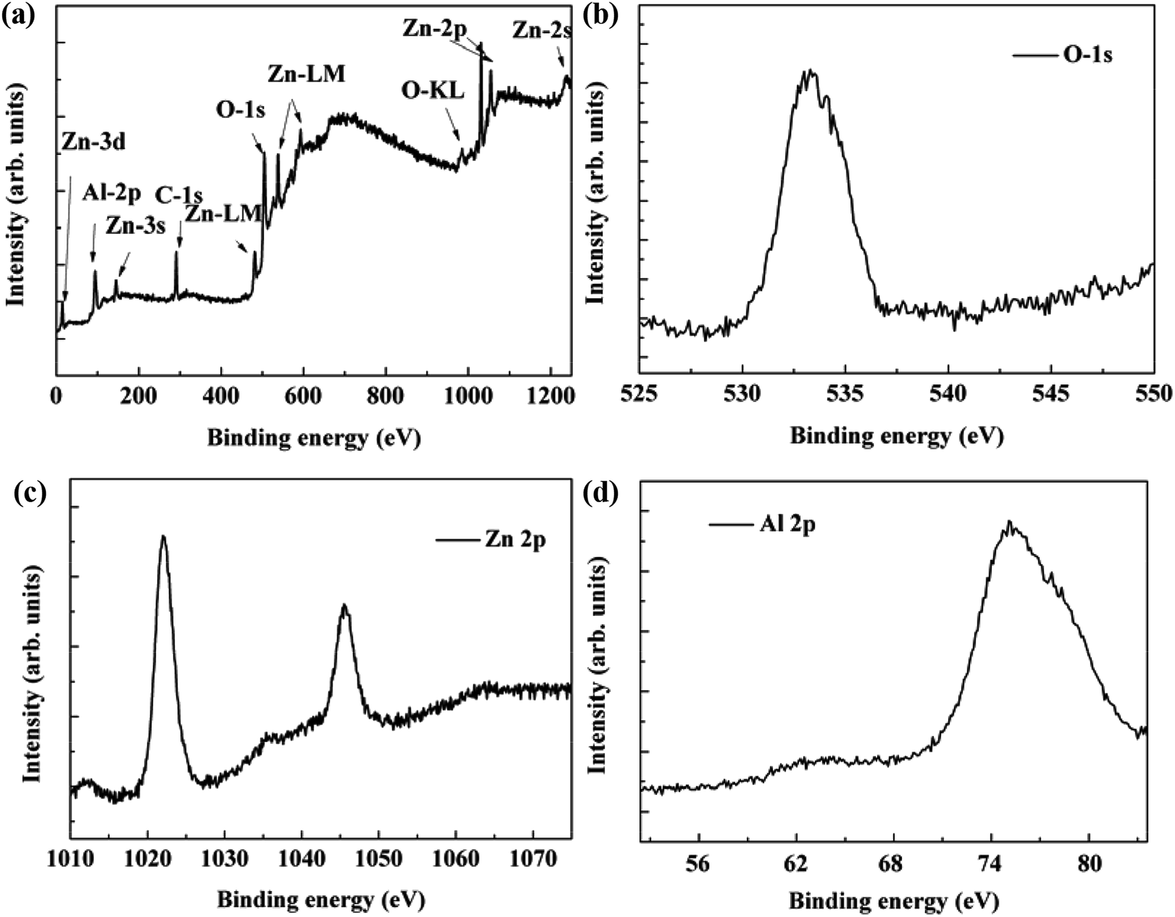 | ||
| Fig. 5 (a) XPS spectra corresponding to the AZO nanowires, (b) O-1s, (c) Zn-2p, and (d) Al-2p core level of AZO nanowires. | ||
Fig. 6 shows the PL spectra of AZO nanostructures in room temperature. The insets of Fig. 6 show the fittings of the PL spectra of crystalline AZO nanostructures in the excitonic emission region. The PL spectra of AZO nanostructures with nanowires, nanobelts and nanoplane-cone are came from a NBE emission in the ultraviolet (UV) region, and two peaks in visible light due to deep-level emission (DLE). Compared with the pure ZnO of 3.37 eV,25,26 the NBE peak shifts to shorter wavelengths (blue shift) with the doping of Al which can be related to Moss Burstein effect.27,28 In addition, Zn2+ ions at their lattice sites by the substitution of Al3+ ions in AZO nanostructures leads to increase of the Fermi level and the broadening of optical band gap. The calculated energy gap values from Tauc formula in pervious section confirm NBE peak blue shift. Similar results are reported by other researchers.21 The AZO nanobelts have a relative stronger UV emission and the AZO nanowires have a relative stronger visible emission (see Fig. 6(d)). The reason is that the band-side excitation of the AZO semiconductor with different morphologies generally occurs near the surface of the AZO nanostructures, resulting in an uneven distribution of the excited carriers. As a result of radiative or non-radiative transitions, excess unbalanced carriers diffuse from the surface to the interior and recombine at the same time to achieve a balanced and uniform distribution. Therefore, the vast majority of excitations in the crystal are confined to the depth of penetration of photons below the surface. After excited by laser, for the AZO nanobelts with larger aspect ratio, most of the non-equilibrium carriers take the radiative recombination, so the ultraviolet radiation is stronger. For the AZO nanoplane-cones with smaller aspect ratio, the unbalanced carriers diffuse from surface to interior, resulting in the trap of a considerable number of electrons and holes and the reduction of the radiation recombination number of effective electrons and holes, so the ultraviolet radiation is weaker and the deep-level radiation stronger. In Fig. 3, the Al at% of the AZO nanobelts is less than other samples. This means that the enhancement of visible light emission of AZO nanowires and nanoplane-cones is due to the enhancement of F–M effect with the increase of Al doping. So the UV radiation is weaker and the deep-level radiation is stronger than AZO nanobelts. Therefore, UV and visible radiation intensity changes significantly with the components, size and morphology of the material.
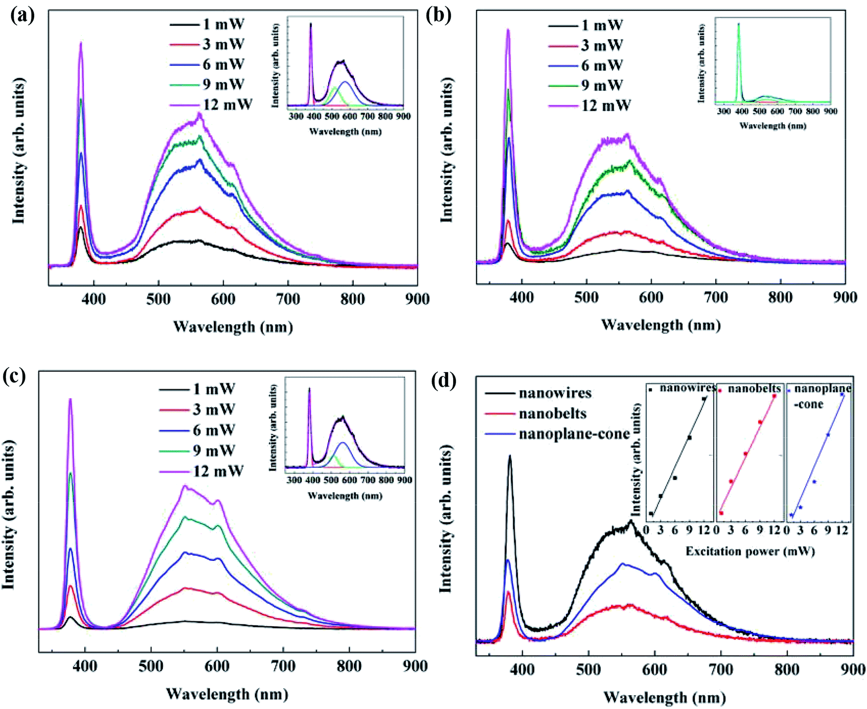 | ||
| Fig. 6 RTPL spectra of AZO nanostructures with different morphologies: (a) nanowires, (b) nanobelts, and (c) nanoplane-cone, respectively. (d) The relationship between the intensity of UV emission peak and excitation power. | ||
In addition, for different excitation laser power, the change of emission band intensity AZO nanowire and nanoplane-cone is uniform, which indicates that the overall growth morphology of AZO nanowire and nanoplane-cone is uniform. The peak ratio of UV and visible emission for three samples: nanowire > nanobelts > nanoplane-cone (see Fig. 6(d)), which shows that the crystallization quality of the nanowire is better than the nanobelts and nanoplane-cone. Noted that intensity of the UV emission peak increases sublinearly with excitation power as shown in the Fig. 6(d) for 325 nm excitations, and no appreciable shift in peak positions is observed. The experimental data can be fitted by the simple power law I ∝ Wμ, where I is the PL intensity, W is the excitation laser power. The dimensionless exponent (μ) represents the radiative recombination mechanism. The μ value satisfies with the relation of 1 < μ < 2 for the free- and bound-exciton emission.29,30 For AZO nanostructures, μ value is 1.16 (for nanowires), 1.08 (for nanobelts) and 1.12 (for nanoplane-cone), respectively. Thus, the obtained value of μ (1< μ < 2) confirms our assignment of the observed emission band in AZO spectra to the free- and bound-exciton emission.
Fig. 7(a–c) shows the LTPL spectra (UV region emission) of AZO nanostructures in the temperature range of 10–273 K. The inset shows the Vis region emission spectra. The results show that three components with center wavelengths at 3.37, 3.36, and 3.32 eV. The peak at 3.37 eV is caused by free excitons (FX = NBE) recombination. The peaks at 3.36 and 3.32 eV can be attributed to bound excitons. The similar phenomenon obtained by H. P. He et al.17 As shown in Fig. 7(a–c), the intensity of emission peak in the UV region decreased drastically with increasing temperature. Fig. 7(e) plots the intensity of the UV emission peak as a function of reciprocal temperature. The presence of two activation energy for thermal quenching is indicative of two competitive nonradiative recombination channels. Because our sample was doped with Al, it is reasonable to assign the UV emission peak to excitons bound to neutral Al donors. Thus, the activation energy may represent the thermal ionization energy of the Al donors. Fig. 7(f) shows the peak positions of the FX, a line and its first longitudinal optical (LO) replica as a function of temperature. When temperature exceeds 90 K, the dominant emission becomes the A line. As temperature further increases, the first LO-phonon replica gradually merges into the A line, resulting in the marked broadening of the NBE emission. The relative intensity of the DL emission peaks at about ∼2.20 eV is strongly reduced. The wavelength locations do not shift. No obvious change was observed for peak position of visible emission in the RTPL spectra.
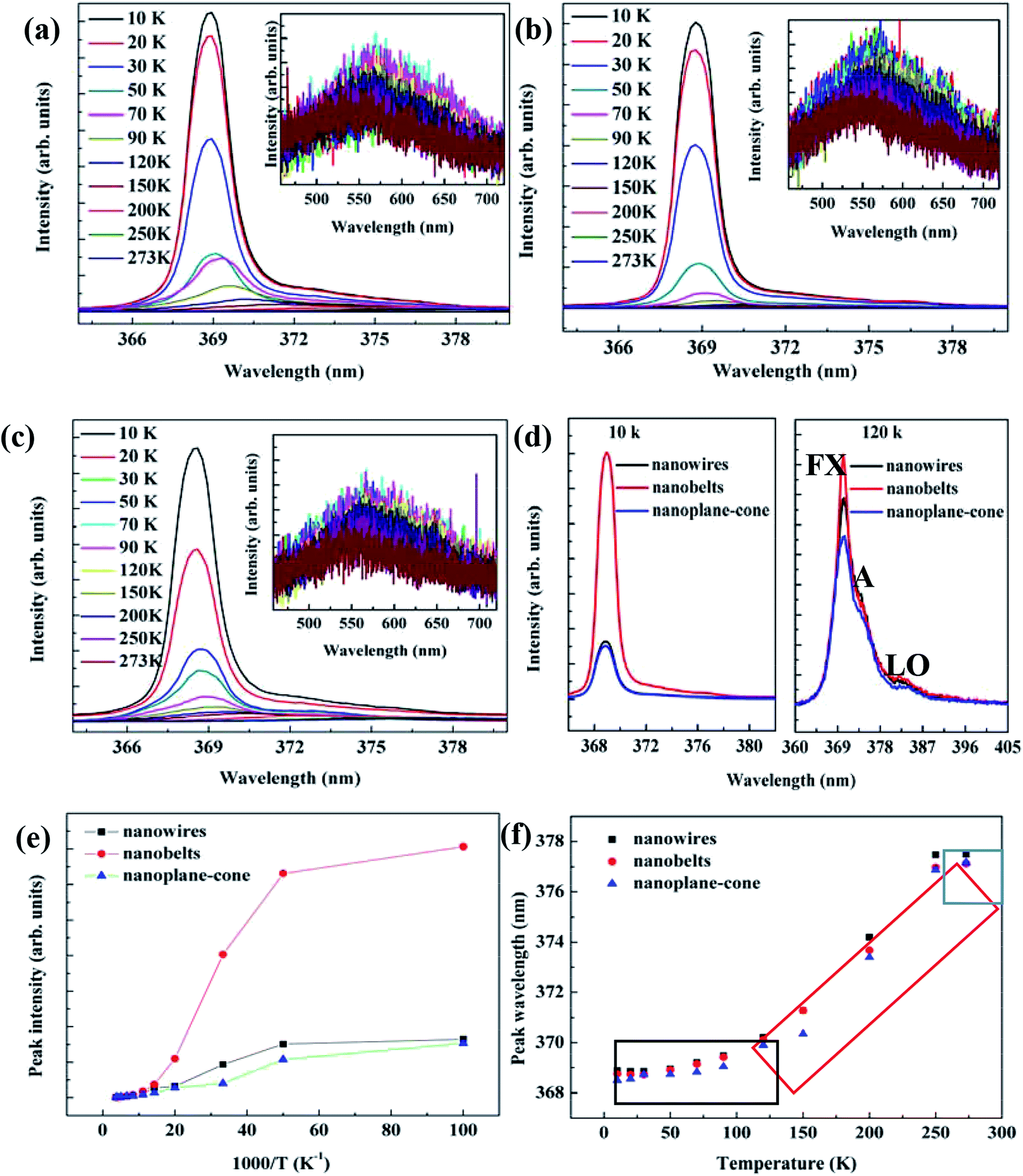 | ||
| Fig. 7 LTPL spectra of AZO nanostructures with different morphologies: (a) nanowires, (b) nanobelts, and (c) nanoplane-cone, respectively. (d) LTPL spectra of AZO nanostructures with different morphologies at 10 K and 120 K. (e) The intensity of the UV emission peak as a function of reciprocal temperature. (f) The peak positions of the FX as a function of temperature. | ||
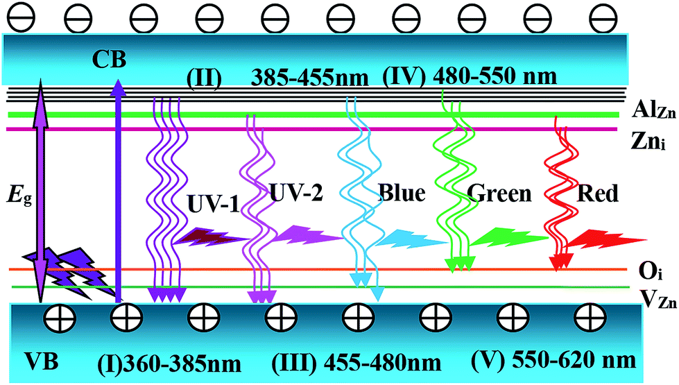
Illustration of the ZnO band, UV and DL emission is shown in Fig. 8. The Vis emission peak was observed in RTPL spectra of the AZO nanostructures. As shown in Fig. 8(I–VI), all emission peaks of the AZO nanostructures can be analyzed by considering the energy band diagram schematically. According to some reports, this visible wavelength emission is excited by the recombination of photogenerated hole with the singly ionized oxygen vacancy site.31–34 The UV emission is derived from the radiated composite luminescence of the forbidden band free excitons, and the blue light emission comes from the fact of the electron transition from Zni to zinc vacancy (VZn) or the top of the VB. For LTPL spectra, when the excitation laser light at 325 nm was launched in the AZO nanostructures, the electrons are excited from the VB to the CB. Hence, the electron density is increased in the FL of Al doping. These electrons are excited and transferred to the bottom of the CB, and recombined with holes in the VB of AZO nanostructures with radiative emission.
 | ||
| Fig. 8 Energy band diagram of the AZO system. | ||
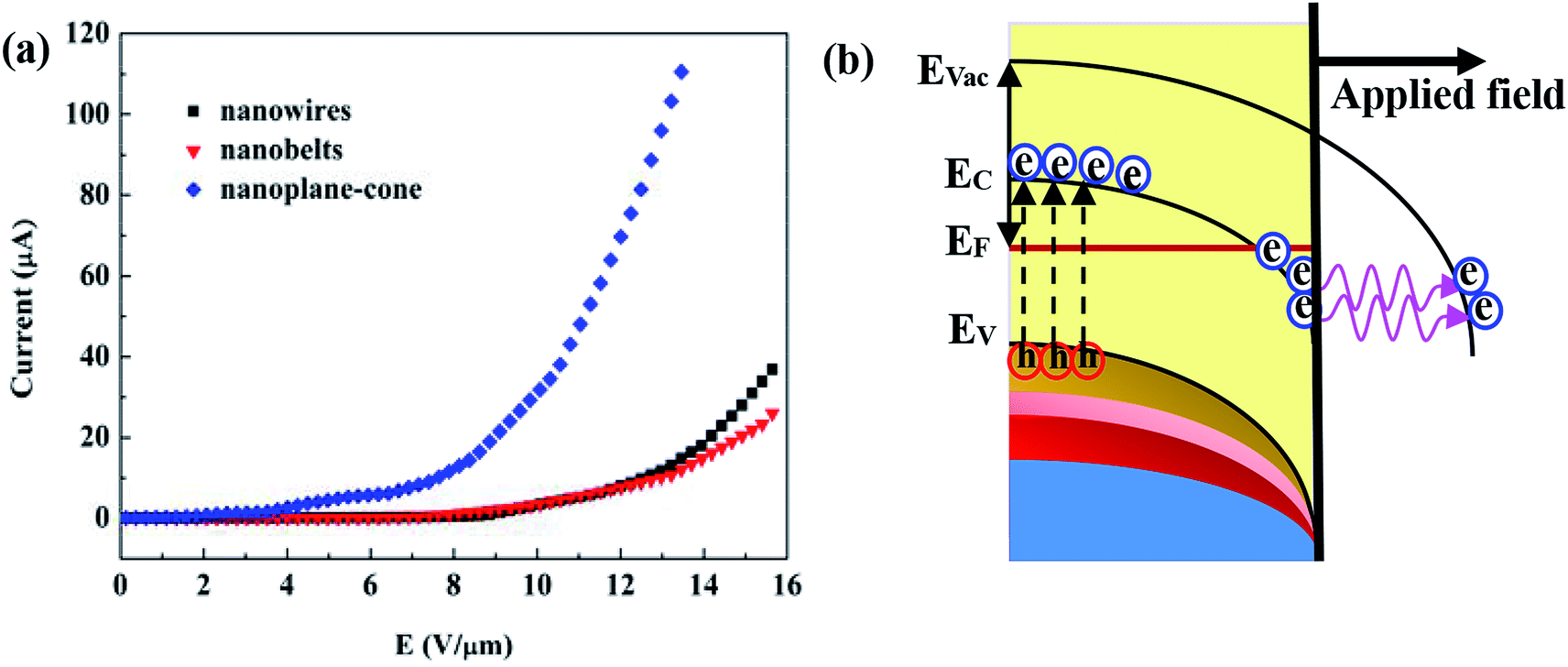
Fig. 9(a) shows the FE current density versus applied field (J–E) of AZO nanostructures with different morphologies. The current density is analyzed as a function of applied field for both samples using Fowler–Nordheim (F–N) theory.35,36 From the J–E curve, the value of the EF, required to draw an EC density of ∼10 μA cm−2, is observed to be ∼1 V μm−1. At a current density of 0.1 μA, the turn-on EF of AZO nanostructures under UV illumination are 4.42 V μm−1 (for nanowires), 5.28 V μm−1 (for nanobelts) and 2.52 V μm−1 (for nanoplane-cone), respectively. To understand the mechanism of the enhanced FE behavior of the AZO nanostructures, the energy band diagrams of AZO nanostructures schematically depicted in Fig. 9(b). Under UV illumination, the electrons transferred from the CB to Fermi energy level. The work function of AZO (4.75 eV) is smaller than ZnO (5.3 eV).37 The decreased work function lowered the turn-on EF. Similar nonlinear J–E plots have been reported for ZnO and doped or decorated ZnO semiconductors, such as Y. G. Fang et al.34 found that the turn-on EF of ZnO nanowires arrays at different reaction decreases from 4.56 to 3.69 V μm−1. S. S. Warule et al. found the turn-on field of ZnO nanopencils is 2.15 V μm−1.35 C. L. Hsu et al.36 found that the FE turn-on EF of Al doped ZnO nanowires are from 2.8 to 1.3 V μm−1. Compare with the present a part of results, the pure and Al doped ZnO nanostructures exhibit a higher applied field value; the reason comes from that the randomly distribution of nanowire arrays better displays the FE performance. In this work, our results showed that the enhanced FE performance of the AZO nanoplane-cone can be attributed to point effect compared to that of other AZO nanostructures. For ZnO nanoplane-cone, its excellent FE property can also attribute to the special morphology. The small tip size and high aspect ratio of nanoplane-cone morphology can generate a high local electric field, which will decrease the FE potential barrier and increase the FE current. The experimental results demonstrate that the FE properties of AZO nanostructures depend on their morphology, structure and crystallinity. The similar phenomenon in ZnO nanograsses has been reported by H. M. Dong et al.37
 | ||
| Fig. 9 (a) Emission current–voltage characteristics of the AZO nanostructures. (b) Band diagrams of AZO nanostructures under UV light. | ||
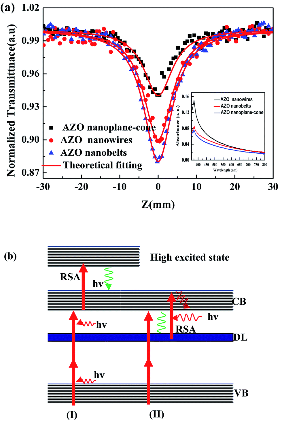
The nonlinear absorption characteristics of AZO nanowires, nanobelts, and nanoplane-cone were studied by Z-scan method with the wavelength at 800 nm and pulse width at 150 fs. Under the laser excitation intensity at 500 nJ, Fig. 10(a) shows the open-aperture Z-scan transmittance curves of AZO nanostructures with the nanowires, nanobelts, and nanoplane-cone morphologies. It can be seen form Fig. 10(a), the open-aperture Z-scan transmittance curves of AZO nanowires, nanobelts, and nanoplane-cone are valley. And the nonlinear absorption mechanism of AZO nanostructures is reverse saturable absorption (RSA). The laser excitation wavelength falls in the wing region of the exciton absorption, satisfying the condition for the occurrence of a three photon absorption (3PA) process (Eg/3 < hν < Eg/2, see inset Fig. 10(a)). The similar analysis process has been reported.38–43 From the experimental results, the 2PA induced conduction band or defect state RSA (two-step 3PA) behavior of AZO nanostructures with different morphologies has been determined. With standard Z scan theory, we extract the effective nonlinear absorption coefficients with the sample approximation. The nonlinear absorption coefficient (α3) was calculated using T3PA = 1/[1 + 2α3Leff(I0/(1 + (z/z0)2))2]1/2.38,39 Where I0 = c/(πr2), c = A/B; Leff = (1 − exp(−2α0L))/2α0, α0 = −(1/L)lnTL. I0 is the laser intensity at the focus; A is the laser energy; B is the pulse width; c is the peak power; r is the focal spot radius; Leff is the effective thickness of the sample; L is the actual thickness of the sample; TL is the linear transmittance of the sample. A fit to above the equation to the open aperture data Z-scan indicates that α3 is 6.48 × 10⁻² cm3 GW−2, 8.72 × 10⁻² cm3 GW−2 and 2.42 × 10⁻² cm3 GW−2 for nanowires, nanobelts, and nanoplane-cone, respectively. The nonlinear absorption coefficient for three AZO nanostructures: nanobelts > nanowire > nanoplane-cone. For AZO nanobelts, the maximum nonlinear absorption coefficient is 8.72 × 10⁻² cm3 GW−2. This is because the incorporation of excess Al into ZnO completely changes the original morphology of the material, and the nonlinear absorption properties of the AZO nanostructures are suppressed. In addition, M. G. Vivas et al.41 reported the reverse saturable, two- and three-photon absorption properties of ZnO at 500 nm, 730 nm and 820 nm, respectively. In contrast, the 3PA coefficient of the AZO nanostructures is larger than that of ZnO in the reference. Because of the Al donor doped ZnO provides more electrons, which lead to value of CB absorption cross-section of AZO nanostructures was increased, thereby the nonlinear absorption was increased. To interpret this intensity dependent nonlinear absorption coefficient, we present a possible optical physical process under 800 nm laser pulse excitation, as shown in Fig. 10(b). The system simultaneously absorbs two identical photons, promoting an electron from ground state to excited state by virtual states. Subsequently, the electron is excited to higher-lying excited state by absorbing another single photon, resulting in 2PA-induced RSA. The similar analysis process has been reported.44–49 Here, the Fig. 10(b) presents the nonlinear absorption mechanism diagram of AZO nanostructures upon direct excitation with 800 nm. In Fig. 10b(I) and (II), the AZO nanostructures have 2PA induced conduction band and 2PA induced defect state RSA at 800 nm in the femtosecond domain. Due to the incorporation of Al, the position of Zn is replaced, the impurity level VO and Zni are increased. And a small amount of Al is incorporated (see Fig. 3), the impurity defect state increases, and the nonlinear absorption of AZO nanostructures is the 2PA induced conduction band or defect state RSA behavior.
 | ||
| Fig. 10 (a) Transmittance curves of AZO nanostructures measured at 800 nm wavelength with 100 fs pulse width. (b) The nonlinear absorption mechanism diagram of AZO nanostructures. | ||
4. Conclusions
In summary, we investigated the structure, PL and FE properties of 1D-AZO nanostructures with three morphologies by a CVD method. The mechanism of the growth, PL and FE properties for AZO nanostructures is analyzed. The enhanced FE properties were achieved by tailoring the morphological design of AZO nanostructures. The FE studies reveal the turn-on EF of AZO nanostructures under UV illumination are 4.42 V μm−1 (for nanowires), 5.28 V μm−1 (for nanobelts) and 2.52 V μm−1 (for nanoplane-cone), respectively. The FE measurements indicated that the nanoplane-cone has a relative smaller turn-on EF than other kinds of samples. The femtosecond open-aperture Z-scan results show that the nonlinear absorption property of AZO nanostructures is RSA properties. And the nonlinear absorption mechanism of AZO nanostructures is 3PA induced RSA. It is calculated that the order of magnitude of the nonlinear absorption coefficient for the all AZO nanostructures is ∼10−2 cm3 GW−2. Our results indicate that AZO nanostructures show great potential as flat panel displays, high brightness electron sources, photoanodes in FE devices and nonlinear optical devices.Conflicts of interest
There are no conflicts to declare.Acknowledgements
This work was supported by the National Natural Science Foundation of China (11504072). University Nursing Program for Young Scholars with Creative Talents in Heilongjiang Province (No. UNPYSCT-2016179).References
- A. B. Djurišić, X. Chen, Y. H. Leung and A. M. C. Ng, ZnO nanostructures: growth, properties and applications, J. Mater. Chem., 2012, 22, 6526–6535 RSC.
- S. Singh, P. Thiyagarajan, K. M. Kant, D. Anita, S. Thirupathiah, N. Rama, B. Tiwari, M. Kottaisamy and M. S. R. Rao, Structure, microstructure and physical properties of ZnO based materials in various forms: bulk, thin film and nano, J. Phys. D: Appl. Phys., 2007, 40, 6312–6327 CrossRef CAS.
- C. Klingshirn, J. Fallert, H. Zhou, J. Sartor, C. Thiele, F. Maier-Flaig, D. Scherder and H. Kalt, 65 years of ZnO research – old and very recent results, Phys. Status Solidi B, 2010, 247, 1424–1447 CrossRef CAS.
- C. L. Hsu and S. J. Chang, Doped ZnO 1D nanostructures: synthesis, properties, and photodetector application, Small, 2014, 10, 4562–4585 CrossRef CAS.
- S. Suwanboon, P. Amornpitoksuk and A. Sukolrat, Dependence of optical properties on doping metal, crystallite size and defect concentration of M-doped ZnO nanopowders (M = Al, Mg, Ti), Ceram. Int., 2011, 37, 1359–1365 CrossRef CAS.
- Y. Zhao, R. J. Tong, M. Q. Chen and F. Xia, Relative humidity sensor based on hollow core fiber filled with GQDs-PVA, Sens. Actuators, B, 2019, 284, 96–102 CrossRef CAS.
- R. Deng, B. Yao, Y. F. Li, T. Yang, B. H. Li, Z. Z. Zhang, C. X. Shan, J. Y. Zhang and D. Z. Shen, Influence of oxygen/argon ratio on structural, electrical and optical properties of Ag-doped ZnO thin films, J. Cryst. Growth, 2010, 312, 1813–1816 CrossRef CAS.
- J. T. Yang, R. Fan, J. Li and F. L. Meng, Hydrogen leakage detectors based on a polymer microfiber decorated with Pd nanoparticles, IEEE Sens. J., 2019, 19(16), 6736–6741 Search PubMed.
- S. J. Young, C. C. Yang and L. T. Lai, Review–growth of Al-, Ga-, and In-doped ZnO nanostructures via a low-temperature process and their application to field emission devices and ultraviolet photosensors, J. Electrochem. Soc., 2017, 164, B3013–B3028 CrossRef CAS.
- B. Paul, B. Singh, S. Ghosh and A. Roy, A comparative study on electrical and optical properties of group III (Al, Ga, In) doped ZnO, Thin Solid Films, 2016, 603, 21–28 CrossRef CAS.
- P. P. Sahay and R. K. Nath, Al-doped ZnO thin films as methanol sensors, Sens. Actuators, B, 2008, 134, 654–659 CrossRef CAS.
- F. Khan, S. Ameen, M. Song and H. S. Shin, Influence of excitation wavelength on photoluminescence spectra of Al doped ZnO films, J. Lumin., 2013, 134, 160–164 CrossRef CAS.
- M. Chen, Z. L. Pei, C. Sun, L. S. Wen and X. Wang, Surface characterization of transparent conductive oxide Al-doped ZnO films, J. Cryst. Growth, 2000, 220, 254–262 CrossRef CAS.
- M. Shirazi, R. S. Dariani and M. R. Toroghinejad, Influence of doping behavior of Al on nanostructure, morphology and optoelectronic properties of Al Doped ZnO thin film grown on FTO substrate, J. Mater. Sci.: Mater. Electron., 2016, 27, 10226–10236 CrossRef CAS.
- Y. Liu, H. Zhang, X. An, C. Gao, Z. Zhang, J. Zhou, M. Zhou and E. Xie, Effect of Al doping on the visible photoluminescence of ZnO nanofibers, J. Alloys Compd., 2010, 506, 772–776 CrossRef CAS.
- A. Mohanta, J. G. S. Simmons Jr, H. O. Everitt, G. Shen, S. M. Kim and P. Kung, Effect of pressure and Al doping on structural and optical properties of ZnO nanowires synthesized by chemical vapor deposition, J. Lumin., 2014, 146, 470–474 CrossRef CAS.
- H. P. He, H. P. Tang, Z. Z. Ye, L. P. Zhu, B. H. Zhao, L. Wang and X. H. Li, Temperature-dependent photoluminescence of quasialigned Al-doped ZnO nanorods, Appl. Phys. Lett., 2007, 90, 023104 CrossRef.
- K. J. Chen, T. H. Fang, F. Y. Hung, L. W. Ji, S. J. Chang, S. J. Young and Y. J. Hsiao, The crystallization and physical properties of Al-doped ZnO nanoparticles, Appl. Surf. Sci., 2008, 254, 5791–5795 CrossRef CAS.
- F. Giovannelli, A. N. Ndimba, P. Diaz-Chao, M. Motelica-Heino, P. I. Raynal, C. Autret and F. Delorme, Synthesis of Al doped ZnO nanoparticles by aqueous coprecipitation, Powder Technol., 2014, 262, 203–208 CrossRef CAS.
- K. H. Kim, T. Umakoshi, Y. Abe, M. Kawamura and T. Kiba, Morphological properties of Al-doped ZnO nano/microstructures, Superlattices Microstruct., 2016, 91, 188–192 CrossRef CAS.
- J. L. Wang, T. Y. Hsieh, P. Y. Yang, C. C. Hwang, D. C. Shye and I. C. Lee, Oxygen annealing effect on field-emission characteristics of hydrothermally synthesized Al-doped ZnO nanowires, Surf. Coat. Technol., 2013, 231, 423–427 CrossRef CAS.
- F. Maldonado and A. Stashans, Al-doped ZnO: Electronic, electrical and structural properties, J. Phys. Chem. Solids, 2010, 71, 784–787 CrossRef CAS.
- Z. X. Lin, Y. A. Zhang, Y. Ye, X. T. Zhou and T. L. Guo, Synthesis and photoelectric properties of ZnO nanostructure with different morphologies via hydrothermal method, Mater. Technol., 2012, 27, 350–354 CrossRef CAS.
- X. Y. Yan, K. X. Zhang, C. B. Yao and Q. H. Li, Ultrafast nonlinear optical properties and optical Kerr effect of In-doped ZnO nanowires, Mater. Lett., 2016, 176, 49–51 CrossRef CAS.
- Y. V. Kaneti, Z. Zhang, J. Yue, Q. M. D. Zakaria, C. Chen, X. Jiang and A. Yua, Crystal plane-dependent gas-sensing properties of zinc oxide nanostructures: experimental and theoretical studies, Phys. Chem. Chem. Phys., 2014, 16, 11471–11480 RSC.
- A. K. Radzimska and T. Jesionowski, Zinc Oxide-from synthesis to application: A review, Materials, 2014, 7, 2833–2881 CrossRef.
- X. J. Wang, I. A. Buyanova, W. M. Chen, C. J. Pan and C. W. Tu, Effects of stoichiometry on defect formation In ZnO epilayers grown by molecular-beam epitaxy: an optically detected magnetic resonance study, J. Appl. Phys., 2008, 103, 023712 CrossRef.
- Y. C. Kong, D. P. Yu, B. Zhang, W. Fang and S. Q. Feng, Ultraviolet-emitting ZnO nanowires synthesized by a physical vapor deposition approach, Appl. Phys. Lett., 2001, 78, 407 CrossRef CAS.
- T. Schmidt, K. Lischka and W. Zulehner, Excitation-power dependence of the near-band-edge photoluminescence of semiconductors, Phys. Rev. B: Condens. Matter Mater. Phys., 1992, 45, 8989–8994 CrossRef.
- H. Yan, Y. Yang, Z. Fu, B. Yang, J. Zuo and S. Fu, Excitation-power dependence of the near-band-edge photoluminescence of ZnO inverse opals and nanocrystal films, J. Lumin., 2008, 128, 245–249 CrossRef CAS.
- K. Saravanan, B. K. Panigrahi, R. Krishnan and K. G. M. Nair, Surface plasmon enhanced photoluminescence and Raman scattering of ultra-thin ZnO–Au hybrid nanoparticles, J. Appl. Phys., 2013, 113, 033512 CrossRef.
- H. P. He, Q. Yang, C. Liu, L. W. Sun and Z. Z. Ye, Size-Dependent Surface Effects on the Photoluminescence in ZnO Nanorods, J. Phys. Chem. C, 2011, 115, 58–64 CrossRef CAS.
- V. A. Fonoberov, K. A. Alim, A. A. Balandin, F. Xiu and J. Liu, Photoluminescence investigation of the carrier recombination processes in ZnO quantum dots and nanocrystals, Phys. Rev. B: Condens. Matter Mater. Phys., 2006, 73, 165317 CrossRef.
- Y. G. Fang, K. M. Wong and Y. Lei, Synthesis and field emission properties of different ZnO nanostructure arrays, Nanoscale Res. Lett., 2012, 7, 197 CrossRef.
- S. S. Warule, N. S. Chaudhari, R. T. Khare, J. D. Ambekar, B. B. Kale and M. A. More, Single step hydrothermal approach for devising hierarchical Ag–ZnO heterostructures with significant enhancement in field emission performance, CrystEngComm, 2013, 15, 7475–7483 RSC.
- C. L. Hsu, C. W. Su and T. J. Hsueh, Enhanced field emission of Al-doped ZnO nanowires grown on a flexible polyimide substrate with UV exposure, RSC Adv., 2014, 4, 2980–2983 RSC.
- H. M. Dong, Y. H. Yang and G. W. Yang, Growth and field emission property of ZnO nanograsses, Mater. Lett., 2014, 115, 176–179 CrossRef CAS.
- Y. D. Zhang, Z. Y. Zhao, C. B. Yao, L. Yang, J. Li and P. Yuan, The nonlinear absorption and optical limiting in phenoxy-phthalocyanines Liquid in nano-and femto-second regime: Experimental studies, Opt. Laser Technol., 2014, 58(6), 207–214 CrossRef CAS.
- X. Y. Yan, C. B. Yao, J. Li, J. Y. Hu, Q. H. Li and S. B. Yang, Structural, photoluminescence and picosecond nonlinear optical effect of In-doped ZnO nanowires, Opt. Mater., 2016, 55, 73–77 CrossRef CAS.
- J. He, Y. Qu, H. Li, J. Mi and W. Ji, Three-photon absorption in ZnO and ZnS crystals, Opt. Express, 2005, 13, 9235–9247 CrossRef CAS.
- M. G. Vivas, T. Shih, T. Voss, E. Mazur and C. R. Mendonca, Nonlinear spectra of ZnO: reverse saturable, two- and three-photon absorption, Opt. Express, 2010, 18(9), 9628–9633 CrossRef CAS.
- U. P. Shaik, P. A. Kumar, M. G. Krishna and S. V. Rao, Morphological manipulation of the nonlinear optical response of ZnO thin films grown by thermal evaporation, Mater. Res. Express, 2014, 1, 046201 CrossRef.
- B. Gu, W. Ji, P. S. Patil, S. M. Dharmaprakash and H. T. Wang, Two-photon-induced excited-state absorption: Theory and experiment, Appl. Phys. Lett., 2008, 92, 091118 CrossRef.
- B. Gu, Y. Sun and W. Ji, Two-photon-induced excited-state nonlinearities, Opt. Express, 2008, 16, 17745–17751 CrossRef.
- B. Gu, K. Lou, H. T. Wang and W. Ji, Dynamics of two-photon-induced three-photon absorption in nanosecond, picosecond, and femtosecond regimes, Opt. Lett., 2010, 35, 417–419 CrossRef CAS.
- R. L. Sutherland, M. C. Brant, J. Heinrichs, J. E. Slagle, D. G. McLean and P. A. Fleitz, Excited state characterization and effective three-photon absorption model of two-photon-induced excited-state absorption in organic push–pull charge-transfer chromophores, J. Opt. Soc. Am. B, 2005, 22, 1939–1948 CrossRef CAS.
- P. A. Kurian, C. Vijayan, C. S. S. Sandeep, R. Philip and K. Sathiyamoorthy, Two-photon-assisted excited state absorption in nanocomposite films of PbS stabilized in a synthetic glue matrix, Nanotechnology, 2007, 18, 075708 CrossRef PubMed.
- T. C. Sabari Girisun, M. Saravanana and V. Rao Soma, Wavelength-dependent nonlinear optical absorption and broadband optical limiting in Au–Fe2O3–rGO nanocomposites, ACS Appl. Nano Mater., 2018, 111, 6337–6348 CrossRef.
- F. Wu, G. L. Zhang, W. Tian, W. J. Chen, G. F. Zhao, S. D. Cao and W. Xie, Two-photon absorption and two-photon assisted excited-state absorption in CdSe0.3S0.7 quantum dots, J. Opt. A: Pure Appl. Opt., 2009, 11, 065206 CrossRef.
| This journal is © The Royal Society of Chemistry 2019 |