
 Open Access Article
 This Open Access Article is licensed under a Creative Commons Attribution-Non Commercial 3.0 Unported Licence
The electrical properties and modulation of g-C3N4/β-As and g-C3N4/β-Sb heterostructures: a first principles study
Bo Liangab,
Yongchao Rao a and
Xiangmei Duan*ab
a and
Xiangmei Duan*ab
aSchool, of Physical Science and Technology, Ningbo University, 315211, China. E-mail: duanxiangmei@nbu.edu.cn
bLaboratory of Clean Energy Storage and Conversion, Ningbo University, Ningbo, 315211, China
First published on 26th November 2019
Abstract
The electronic properties of the g-C3N4/β-As and g-C3N4/β-Sb heterojunctions are investigated via density functional theory. We find that both heterostructures are indirect band gap semiconductors that, when applied to a photocatalytic device, will suffer from inefficient light emission. Fortunately, the band gap of the two junctions can be adjusted by external biaxial strain. As strain increases from compression to extensive, both compounds undergo a transition from metals, indirect semiconductors to direct semiconductors. Moreover, due to the charge transfer, each junction forms a large built-in electric field, which helps to prevent the recombination of electrons and holes. Our results are expected to widen the potential applications of these heterojunctions in nanodevices.
1. Introduction
The successful exfoliation of single layer of graphite1 led a revolution in two dimensional (2D) materials, which attracted widespread attention in the next few years for their special properties and potential applications. Graphene has excellent electron mobility,2,3 high thermal stability4 and conductivity,5,6 great mechanical7,8 and optical9 properties. However, the lack of band gap seriously restricts its actual utilization in microelectronic devices. Researchers have been working on finding other 2D materials. Recently, hexagonal boron nitride (h-BN),10,11 transition metal dichalcogenide (TMD),12–14 graphitic carbon nitride,15–18 and phosphorene19–21 have been synthesized successfully. Thereafter, ultrathin 2D van der Waals heterojunctions and their devices have received extensive attention.22,23Among the allotropes of the non-metallic carbon nitride, graphitic C3N4 (g-C3N4) is the most stable phase under ambient conditions.24 It exhibits the characteristic of semiconductor (with a band gap of 2.7 eV25), and is non-toxic, visible light responsive and easy to synthesize.26–28 In addition, g-C3N4 has caused great concern due to its conceivable usage in electronic devices and optoelectronic conversion.
For bulk arsenic and antimony, the most stable allotrope is beta gray arsenic and beta gray antimony, respectively. Both are buckled honeycomb structure analogous to blue phosphorus.29 And their monolayer counterparts are known as gray arsenene (β-As) and gray antimonene (β-Sb), respectively. β-As and β-Sb sheets have been experimentally synthesized,30–33 with a corresponding indirect band gap of 2.49 and 2.28 eV,30 as well as considerable carrier mobility.34–36 It is critical to have a tunable band gap for semiconductor materials, especially when applied to nanodevices. Previous studies have reported that the electronic structure of few-layer arsenic and antimony nanosheets depends sensitively on the number of layers, stacking modes and defects.36–40 Meanwhile, β-As or β-Sb can be converted into direct band gap semiconductors under electric field and biaxial strain.37,41,42 An interesting idea arises: can the electronic properties of β-As and β-Sb based heterostructures be modulated under strain?
In this paper, the electronic properties of g-C3N4/β-As and g-C3N4/β-Sb heterostructures are systematically investigated by using first-principles calculations. We find that the stable heterostructures can be readily formed due to the slight lattice mismatch between the compounds. The charge transfer between each junction results in a built-in electric field, which helps to prevent the recombination of electrons and holes. The heterostructures are indirect band gap semiconductors, however, their electronic properties could be tuned by the biaxial strain (ε).
2. Calculation methods
All the calculations are performed using the plane-wave basis Vienna Ab initio Simulation Package (VASP) code. The exchange–correlation potentials are described through the Perdew–Burke–Ernzerhof (PBE) functional within the generalized gradient approximation (GGA) formalism. A damped van der Waals correction (DFT-D2) based on Grimme's scheme is also incorporated to better describe the non-bonding interaction between the different layers.43 The vacuum region is 20 Å to avoid the spurious interaction caused by the periodic boundary condition. A Morkhorst-pack k points mesh of 5 × 5 × 1 and 11 × 11 × 1 is used to sample the Brillouin zone for geometry optimization and calculating the density of states, respectively. The cutoff energy of the plane–wave is set to be 500 eV. All of the self-consistent loops are iterated until the total energy difference of the systems between the adjacent iterating steps less than 10−5 eV, and the structures are fully relaxed with a force tolerance of 0.005 eV Å−1.Binding energy, Eb, can be used to present the structural stability of the heterostructure system. For instance, the binding energy of g-C3N4 and β-As is defined as
| Eb = (Eg-C3N4/β-As − Eg-C3N4 − Eβ-As)/N |
The charge density difference is determined by subtracting the electronic charge of the corresponding isolated compositions from the heterojunctions, for g-C3N4/β-Sb, that is, Δρ = ρg-C3N4/β-Sb − ρg-C3N4 − ρβ-Sb, where ρg-C3N4/β-Sb, ρg-C3N4, and ρβ-Sb are the charge density of the corresponding g-C3N4/β-Sb heterostructure, g-C3N4 and β-Sb sheet. The amount of transferred charge ΔQ(z) is calculated by 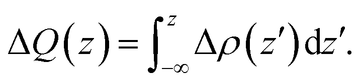
The biaxial strain is defined as ε = (l − l0)/l0 × 100%, where l and l0 is the strained and original lengths of the monolayer along one of strain direction. The sample is compressed or tensile in two distinct directions with the same strain level.
3. Results and discussion
As shown in Table 1, the optimized lattice parameters of g-C3N4, β-As, and β-Sb monolayers are 7.13, 3.62 and 4.06 Å, respectively, in good agreement with the previous theoretical and experimental reports (7.13, 3.68 and 4.01 Å).25,30,34 For the three kinds of sheets, GGA-PBE shows the band gaps of 1.20, 1.63, and 1.12 eV, which agree well with the reported data (1.19, 1.64, and 1.18 eV).34,44,45| g-C3N4 | β-As | β-Sb | |
|---|---|---|---|
| a (Å) | 7.13 (7.13)b | 3.62 (3.68)c | 4.06 (4.01)d |
| Eg (eV) | 1.20 (1.19)e | 1.63 (1.64)c | 1.12 (1.18)f |
To simulate the g-C3N4/β-As and g-C3N4/β-Sb heterostructures, a 2 × 2 supercell for β-As and a  cell for β-Sb are used separately to match the 1 × 1 g-C3N4 unit cell. The lattice mismatch is only 1.54% (1.37%) respectively between β-As (β-Sb) and g-C3N4, which should be suitable for building hybrid structures. The top and side views of g-C3N4/β-As and g-C3N4/β-Sb heterostructures are illustrated in Fig. 1. The g-C3N4 and β-As sheets remain their pristine geometries with a vertical distance of 3.44 Å. While in the junction of g-C3N4/β-Sb, the layer g-C3N4 tilts slightly, the average distance between the two counterparts is 3.42 Å. Therefore, the heterojunctions are connected by van der Waals interaction. The binding energy is calculated to be −37.14 meV and −42.86 meV for g-C3N4/β-As and g-C3N4/β-Sb, respectively, indicating the stability of both heterojunctions. The strength of the interaction is stronger than that of graphene/β-As (graphene/β-Sb) heterojunctions, in which Eb is −29.70 meV or −39.62 meV, as reported by similar DFT calculations.46,47
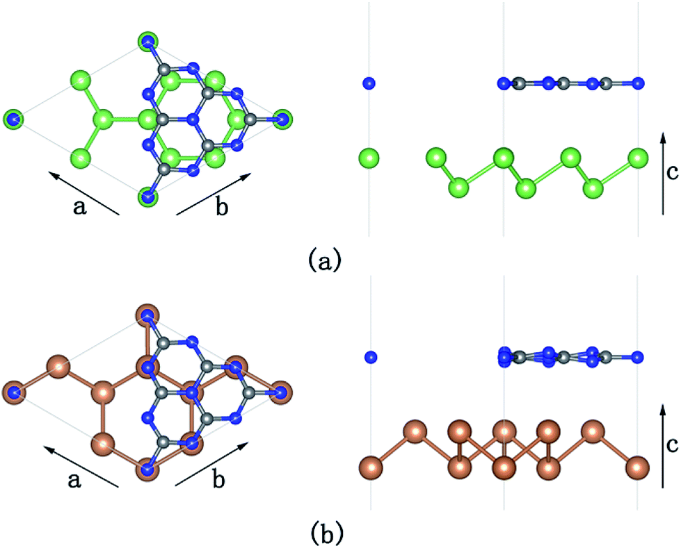 | ||
| Fig. 1 Top (left panel) and side (right panel) views of g-C3N4/β-As (a) and g-C3N4/β-Sb (b). Blue, gray, green, and brown spheres represent the N, C, As, and Sb atoms, respectively. | ||
Band structure and density of states for the hybrid g-C3N4/β-As and g-C3N4/β-Sb are shown in Fig. 2. The PBE calculation gives an indirect band gap of 1.24 eV for g-C3N4/β-As and 0.83 eV for g-C3N4/β-Sb. For the former, the VBM locates at Γ point and CBM at K point. While for the latter, the VBM is located at Γ too and CBM at M. Intriguingly, a large dispersion of band nears the VBM of the g-C3N4/β-Sb can be observed, indicating the high mobility of photogenerated holes. While both the CBM and VBM of g-C3N4/β-As are relatively localized, meaning a low carrier mobility.
 | ||
| Fig. 2 The band structure and DOS of g-C3N4/β-As (a) and g-C3N4/β-Sb (b). | ||
To quantitatively understand carrier migration, we calculate the effective mass of charge carriers by the formula 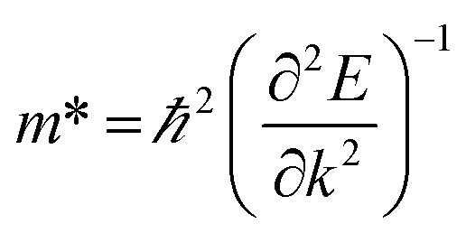 and list the results in Table 2. Generally, the values of effective masses along different directions have a large difference in g-C3N4/β-As and g-C3N4/β-Sb, confirming the obvious anisotropy in the heterojunctions. For β-As junction, the great values of holes,
  along the Γ–K and Γ–M directions, and the mass of electrons,
  along the K–M direction, reveal poor mobility of carrier migration. Fortunately, the mass
  along the Γ–K direction is small, which provides the possibility for potential application of this material. In the case of g-C3N4/β-Sb, the effective masses of
  along the Γ–K and Γ–M directions are reduced to 0.78 and 0.43 in comparison to the two separate sheets, which is expected to be used in photo-electronic devices.
|
|
|
|
|
|
|---|---|---|---|---|---|
| β-As | — | 0.57 | — | 0.53 | 0.71 |
| β-Sb | 0.49 | — | — | 0.92 | 0.48 |
| g-C3N4 | 0.83 | — | 2.86 | 4.87 | 2.66 |
| g-C3N4/β-As | 0.84 | — | 2.40 | 4.71 | 3.69 |
| g-C3N4/β-Sb | — | 0.62 | 4.29 | 0.78 | 0.43 |


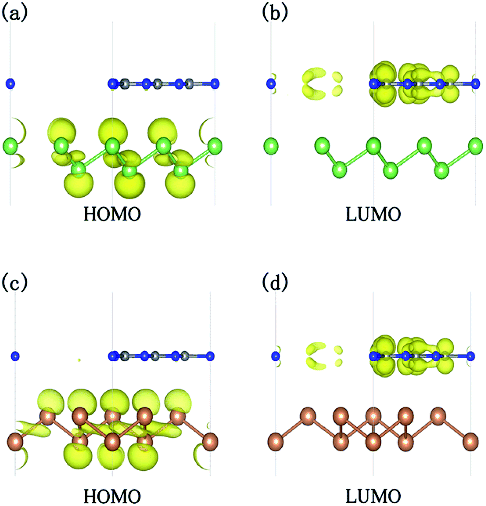
From the partial density of states (PDOS) plots (shown in Fig. 2) of the two heterostructures, it can be seen that the VBM of g-C3N4/β-As is mainly contributed by the 2p states of N atoms and slightly by the 2p states of C atoms, its CBM consists of the 2p states of C atoms and N atoms, i.e. the VBM and CBM are mostly contributed by g-C3N4 side. In the case of g-C3N4/β-Sb, the VBM is attributed by 5p states of the Sb atoms, in contrast, the CBM is composed of the 2p states of C atoms and N atoms. More intuitively, the orbital diagrams in Fig. 3 shows that the VBM and CBM of g-C3N4/β-As are both located in the monolayer g-C3N4 [see (a) and (b)].
 | ||
| Fig. 3 The charge density corresponding to the HOMO and LUMO states for g-C3N4/β-As (a and b) and g-C3N4/β-Sb (c and d) with an isosurface value of 0.004 e Å−3. | ||
The band edge alignment tells that g-C3N4/β-As is a type-I heterojunction, with the HOMO and LUMO locating in the same material of heterostructure. Whereas, the HOMO and LUMO of g-C3N4/β-Sb are located in different parts. The HOMO (VBM at Γ point) is mainly composed of the Sb atoms, while the LUMO (CBM at M point) is primarily contributed by the C atoms and N atoms from g-C3N4 side, indicating a type-II heterojunction, which has lower carrier recombination rate due to the separation of photogenerated electrons and holes, therefore it has higher carrier mobility and stronger photocatalytic activity.
We further investigate the charge density difference and the amount of transferred charge. Fig. 4(a) and (c) present the redistribution of charge density in two systems. Additionally, the vertical lateral charge transfer is shown in Fig. 4(b and d). We note that for g-C3N4/β-Sb junction, the charge density is redistributed by forming triangular shaped electron- and hole-rich regions, i.e., an electron–hole puddle within the β-Sb layer. The formation mechanism of electron–hole enrichment zone is due to the inhomogeneous planar g-C3N4 substrate. The planar averaged charge density difference in Fig. 4(b and d) shows that the g-C3N4 layer donates electrons to β-As or β-Sb side. Thus, the charge transfer between β-As or β-Sb and g-C3N4 introduces a built-in electric field, which produces a driving force to separate the photogenerated carriers to different monolayers.
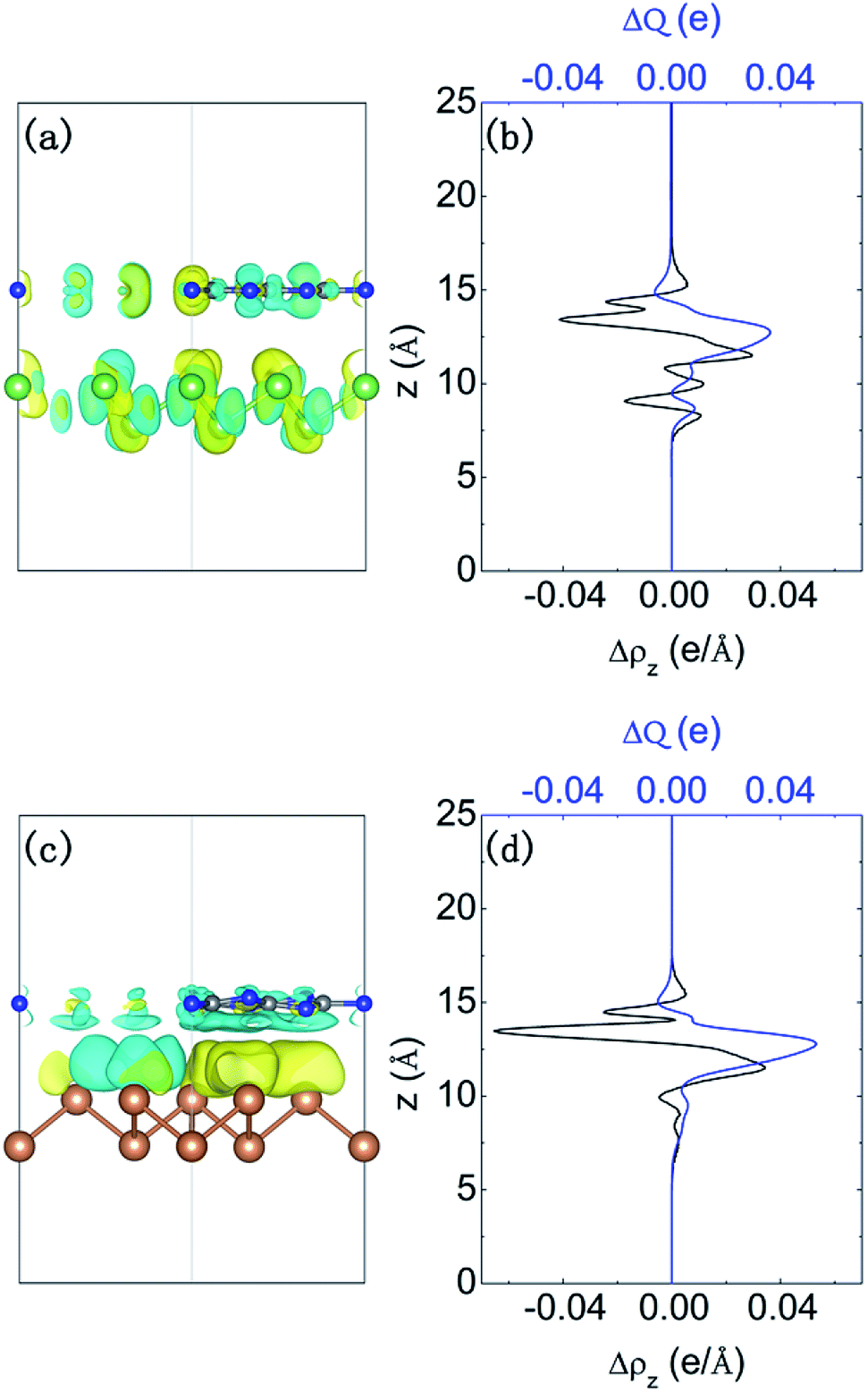 | ||
| Fig. 4 Charge density difference (a) and (c), with an isosurface value of 0.0002 e Å−3, the plane averaged differential charge density along the z direction Δρ and the amount of transferred charge ΔQ (b and d) for g-C3N4/β-As and g-C3N4/β-Sb junctions. | ||
It is well known that strain can significantly adjust the electronic properties of 2D materials, especially in the application of band engineering and device design. Since the systems g-C3N4/β-As and g-C3N4/β-Sb are all indirect band gap semiconductors, when applied to a photocatalytic device, they will suffer from poorly efficient light emission. We next study how the geometric stability and electronic properties of heterojunctions change under external biaxial strain, for the intact strain range, we then focus on their band regulation. Fig. 5(a) presents the stress varies with the strain for the two junctions. It can be seen that g-C3N4/β-As keeps its structure intact under the strain from 12% compressive to 8% tensile, while g-C3N4/β-Sb can sustain a biaxial compressive and tensile strain up to 10% means that the structure of the membrane is robust under a strain.
 | ||
| Fig. 5 (a) The stress of the junctions as a function of strain. Band gaps change under different biaxial strain of g-C3N4/β-As (b) and g-C3N4/β-Sb (c). Three regions are defined by the band type of the materials. m stands for metal, d and i represent the direct and indirect band gap of the semiconductors, respectively. The strain dependence of the band gap for isolated β-As and β-Sb are included for comparison. | ||
Combining the Fig. 5(b) and (c), it can be seen that the band gap of g-C3N4/β-As and g-C3N4/β-Sb junctions have a significant regulation under external biaxial strain (ε). When ε is in the range of [−6, 5], g-C3N4/β-As has an indirect band gap, which turns into a direct one when ε increases above 5%. A further decrease of ε less than −6%, the junction undergoes a transition from a semiconductor to a metal. Similarly, the g-C3N4/β-Sb exhibits metallic property when ε ≤ −6%. While it is still indirect band gap semiconductor in the strain range of [−5, 9]. When ε is in [−6, −5] and [9, 10], the junction experiences a transition from an indirect band gap semiconductor to a direct one. To figure out which part of the compounds dominate the change of the band structure under strain. We systematically investigate the electronic behavior of g-C3N4, β-As and β-Sb monolayers as a function of strain. As illustrated in Fig. 5(b) and (c), intriguingly, the variation trends of band gap for g-C3N4/β-As and g-C3N4/β-Sb are similar to the β-As and β-Sb, indicating β-As and β-Sb play a central role in the transition of the electronic characteristic of the junctions.
To reveal the mechanism for the transition of an indirect band gap semiconductor to a direct band gap, the electronic structure of g-C3N4/β-As at ε = 6% and g-C3N4/β-Sb at ε = 10% is compared with those of the unstrained system, respectively. For the junction containing β-As (β-Sb), the strain changes the CBM originally located at K (M) point to Γ point, while the location of VBM remains at Γ point. Moreover, the carrier distributions of the HOMO and LUMO states, as shown in Fig. 6, indicates the separation of electrons and holes for both systems, which is beneficial to prevent the recombination of the photogenerated carriers.
 | ||
| Fig. 6 The charge density distribution of the HOMO and LUMO states for g-C3N4/β-As at ε = 6% (a and b) and for g-C3N4/β-Sb under ε = 10% (c and d). The isosurface value is 0.004 e Å−3. | ||
4. Conclusion
In summary, we have systematically investigated the electronic properties of the g-C3N4/β-As and g-C3N4/β-Sb junctions by density functional theory. The heterojunctions exhibit various electronic properties. Firstly, the g-C3N4/β-As is a type-I heterostructure, while the complex g-C3N4/β-Sb is a type-II junction. Secondly, the band gap of g-C3N4/β-Sb junction is significantly reduced, which promotes its adsorption of visible light. Thirdly, a certain amount of charge transfers between the layers of the two heterojunctions, and a large built-in electric field is formed to block the recombination of electrons and holes. Particularly, both compounds undergo a transition from the metals, the indirect semiconductors to direct semiconductors under strain. Our findings are beneficial to the development of high performance nanodevices in the future.Conflicts of interest
There are no conflicts to declare.Acknowledgements
This research is supported by the Natural Science Foundation of China (grant no. 11574167 and 11874033) and the KC Wong Magna Foundation in Ningbo University.References
- K. S. Novoselov, A. K. Geim, S. V. Morozov, D. Jiang, Y. Zhang, S. V. Dubonos, I. V. Grigorieva and A. A. Firsov, Science, 2004, 306, 666–669 CrossRef CAS PubMed.
- K. S. Novoselov, A. K. Geim, S. V. Morozov, D. Jiang, M. I. Katsnelson, I. V. Grigorieva, S. V. Dubonos and A. A. Firsov, Nature, 2005, 438, 197–200 CrossRef CAS PubMed.
- K. I. Bolotin, K. J. Sikes, Z. Jiang, M. Klima, G. Fudenberg, J. Hone, P. Kim and H. L. Stormer, Solid State Commun., 2008, 146, 351–355 CrossRef CAS.
- H. Y. Nan, Z. H. Ni, J. Wang, Z. Zafar, Z. X. Shi and Y. Y. Wang, J. Raman Spectrosc., 2013, 44, 1018–1021 CrossRef CAS.
- A. A. Balandin, S. Ghosh, W. Bao, I. Calizo, D. Teweldebrhan, F. Miao and C. N. Lau, Nano Lett., 2008, 8, 902–907 CrossRef CAS PubMed.
- H. Malekpour, K. H. Chang, J. C. Chen, C. Y. Lu, D. L. Nika, K. S. Novoselov and A. A. Balandin, Nano Lett., 2014, 14, 5155–5161 CrossRef CAS PubMed.
- C. Lee, X. Wei, J. W. Kysar and J. Hone, Science, 2008, 321, 385–388 CrossRef CAS PubMed.
- R. Faccio, P. A. Denis, H. Pardo, C. Goyenola and Á. W. Mombrú, J. Phys.: Condens. Matter, 2009, 21, 285304 CrossRef PubMed.
- L. A. Falkovsky, J. Phys.: Conf. Ser., 2008, 129, 012004 CrossRef.
- K. Watanabe, T. Taniguchi and H. Kanda, Nat. Mater., 2004, 3, 404–409 CrossRef CAS PubMed.
- L. Song, L. Ci, H. Lu, P. B. Sorokin, C. Jin, J. Ni, A. G. Kvashnin, D. G. Kvashnin, J. Lou, B. I. Yakobson and P. M. Ajayan, Nano Lett., 2010, 10, 3209–3215 CrossRef CAS PubMed.
- Q. H. Wang, K. Kalantar-Zadeh, A. Kis, J. N. Coleman and M. S. Strano, Nat. Nanotechnol., 2012, 7, 699 CrossRef CAS PubMed.
- M. Chhowalla, H. S. Shin, G. Eda, L.-J. Li, K. P. Loh and H. Zhang, Nat. Chem., 2013, 5, 263 CrossRef PubMed.
- Y.-C. Rao, S. Yu and X.-M. Duan, Phys. Chem. Chem. Phys., 2017, 19, 17250–17255 RSC.
- A. Thomas, A. Fischer, F. Goettmann, M. Antonietti, J.-O. Müller, R. Schlögl and J. M. Carlsson, J. Mater. Chem., 2008, 18, 4893–4908 RSC.
- G. Gao, Y. Jiao, F. Ma, Y. Jiao, E. Waclawik and A. Du, Phys. Chem. Chem. Phys., 2015, 17, 31140–31144 RSC.
- S. Yu, Y.-C. Rao, H.-H. Wu and X.-M. Duan, Phys. Chem. Chem. Phys., 2018, 20, 27970–27974 RSC.
- Y.-C. Rao, Z.-Q. Chu, X. Gu and X.-M. Duan, Comput. Mater. Sci., 2019, 161, 53–57 CrossRef CAS.
- H. Liu, A. T. Neal, Z. Zhu, Z. Luo, X. Xu, D. Tománek and P. D. Ye, ACS Nano, 2014, 8, 4033–4041 CrossRef CAS PubMed.
- L. Kou, C. Chen and S. C. Smith, J. Phys. Chem. Lett., 2015, 6, 2794–2805 CrossRef CAS PubMed.
- Y.-C. Rao, P. Zhang, S.-F. Li, X.-M. Duan and S.-H. Wei, Phys. Chem. Chem. Phys., 2018, 20, 12916–12922 RSC.
- Y. Deng, Z. Luo, N. J. Conrad, H. Liu, Y. Gong, S. Najmaei, P. M. Ajayan, J. Lou, X. Xu and P. D. Ye, ACS Nano, 2014, 8, 8292–8299 CrossRef CAS PubMed.
- W. Hu and J. Yang, Comput. Mater. Sci., 2016, 112, 518–526 CrossRef CAS.
- D. M. Teter and R. J. Hemley, Science, 1996, 271, 53–55 CrossRef CAS.
- X. Wang, K. Maeda, A. Thomas, K. Takanabe, G. Xin, J. M. Carlsson, K. Domen and M. Antonietti, Nat. Mater., 2008, 8, 76 CrossRef PubMed.
- J. Zhang, X. Chen, K. Takanabe, K. Maeda, K. Domen, J. D. Epping, X. Fu, M. Antonietti and X. Wang, Angew. Chem., Int. Ed., 2010, 49, 441–444 CrossRef CAS PubMed.
- J. Liu, T. Zhang, Z. Wang, G. Dawson and W. Chen, J. Mater. Chem., 2011, 21, 14398–14401 RSC.
- S. Martha, A. Nashim and K. M. Parida, J. Mater. Chem. A, 2013, 1, 7816–7824 RSC.
- S. Zhang, M. Xie, F. Li, Z. Yan, Y. Li, E. Kan, W. Liu, Z. Chen and H. Zeng, Angew. Chem., Int. Ed., 2016, 55, 1666–1669 CrossRef CAS PubMed.
- G. Pizzi, M. Gibertini, E. Dib, N. Marzari, G. Iannaccone and G. Fiori, Nat. Commun., 2016, 7, 12585 CrossRef CAS PubMed.
- R. Gusmão, Z. Sofer, D. Bouša and M. Pumera, Angew. Chem., 2017, 129, 14609–14614 CrossRef.
- Y. Wang, P. Huang, M. Ye, R. Quhe, Y. Pan, H. Zhang, H. Zhong, J. Shi and J. Lu, Chem. Mater., 2017, 29, 2191–2201 CrossRef CAS.
- X. Wu, Y. Shao, H. Liu, Z. Feng, Y.-L. Wang, J.-T. Sun, C. Liu, J.-O. Wang, Z.-L. Liu, S.-Y. Zhu, Y.-Q. Wang, S.-X. Du, Y.-G. Shi, K. Ibrahim and H.-J. Gao, Adv. Mater., 2017, 29, 1605407 CrossRef PubMed.
- C. Kamal and M. Ezawa, Phys. Rev. B: Condens. Matter Mater. Phys., 2015, 91, 085423 CrossRef.
- M. Fortin-Deschênes, O. Waller, T. O. Menteş, A. Locatelli, S. Mukherjee, F. Genuzio, P. L. Levesque, A. Hébert, R. Martel and O. Moutanabbir, Nano Lett., 2017, 17, 4970–4975 CrossRef PubMed.
- K. Iordanidou, J. Kioseoglou, V. V. Afanas'ev, A. Stesmans and M. Houssa, Phys. Chem. Chem. Phys., 2017, 19, 9862–9871 RSC.
- S. Zhang, Z. Yan, Y. Li, Z. Chen and H. Zeng, Angew. Chem., 2015, 127, 3155–3158 CrossRef.
- Z. Zhang, J. Xie, D. Yang, Y. Wang, M. Si and D. Xue, Appl. Phys. Express, 2015, 8, 055201 CrossRef.
- L. Yang, Y. Song, W. Mi and X. Wang, RSC Adv., 2016, 6, 66140–66146 RSC.
- X. Sun, Y. Liu, Z. Song, Y. Li, W. Wang, H. Lin, L. Wang and Y. Li, J. Mater. Chem. C, 2017, 5, 4159–4166 RSC.
- H. Shu, Y. Li, X. Niu and J. Guo, J. Mater. Chem. C, 2018, 6, 83–90 RSC.
- L. Kou, Y. Ma, X. Tan, T. Frauenheim, A. Du and S. Smith, J. Phys. Chem. C, 2015, 119, 6918–6922 CrossRef CAS.
- S. Grimme, J. Comput. Chem., 2006, 27, 1787–1799 CrossRef CAS PubMed.
- F. Wu, Y. Liu, G. Yu, D. Shen, Y. Wang and E. Kan, J. Phys. Chem. Lett., 2012, 3, 3330–3334 CrossRef CAS.
- D. Singh, S. K. Gupta, Y. Sonvane and I. Lukačević, J. Mater. Chem. C, 2016, 4, 6386–6390 RSC.
- W. Li, T.-X. Wang, X.-Q. Dai, X.-L. Wang, Y.-Q. Ma, S.-S. Chang and Y.-N. Tang, Phys. E, 2017, 88, 6–10 CrossRef CAS.
- H. V. Phuc, N. N. Hieu, B. D. Hoi, L. T. T. Phuong, N. V. Hieu and C. V. Nguyen, Superlattices Microstruct., 2017, 112, 554–560 CrossRef CAS.
| This journal is © The Royal Society of Chemistry 2019 |