
 Open Access Article
 This Open Access Article is licensed under a Creative Commons Attribution-Non Commercial 3.0 Unported Licence
Solution-processable reduced graphene oxide template layer for molecular orientation control of organic semiconductors†
Keitaro Yamada,
Michitaka Okamoto,
Minori Sakurai,
Tomoyoshi Suenobu and
Ken-ichi Nakayama*
and
Ken-ichi Nakayama*
Department of Material and Life Science, Osaka University, 2-1 Yamadaoka, Suita, Osaka, Japan. E-mail: nakayama@mls.eng.osaka-u.ac.jp
First published on 15th October 2019
Abstract
A reduced graphene oxide (rGO) film is first applied to a surface template layer to control the molecular orientation of crystalline organic semiconductors. The ultrathin and ultrasmooth rGO layer was successfully prepared on a substrate without a transfer process by spin-coating a carefully purified GO aqueous dispersion. This rGO layer exhibited a strong templating effect rivaling monolayer graphene, inducing a face-on orientation of copper phthalocyanine molecules leading to significant improvement of vertical carrier mobilities. The highly-conductive and transparent rGO film does not hamper charge transport at the interface and photoabsorption unlike conventional templating materials. This method can be widely used for vertical organic devices that require high carrier mobilities and strong photoabsorption/emission.
Introduction
Most crystalline organic semiconductors exhibit anisotropic optoelectronic properties owing to their planar molecular structures. Moreover, charge carrier transport governed by the overlap of π-orbitals benefits the π–π stacking direction.1 Therefore, the molecular orientation with respect to the substrate surface significantly affects the performance of organic semiconductor devices. In lateral devices, charge carriers travel along the substrate surface; thus, an edge-on molecular orientation with molecular planes perpendicular to the substrate benefits in-plane charge transport. Surface treatment techniques with hydrophobic self-assembled monolayers have been employed to induce such edge-on orientation and very high carrier mobility (exceeding 10 cm2 V−1 s−1).2 In contrast, in vertical devices, charge carriers travel vertically to the substrate surface. For vertical charge transport, a face-on molecular orientation with molecular planes parallel to the substrates is ideal; however, because there is no standard method to obtain face-on oriented and highly crystalline films, vertical carrier mobility is generally ∼10−3 cm2 V−1 s−1, i.e., much lower than that of lateral devices. This is referred to as the vertical mobility problem.3 Owing to low mobility, very thin organic films are required to achieve better electrical properties, assuming film structures are not influenced by film thickness, making large-area mass production difficult. Moreover, light absorption and emission depend on the direction of the transition dipoles lying on the molecular planes.4 A face-on orientation aids efficient light extraction in organic light-emitting diodes (OLEDs)5 and strong photoabsorption in organic photovoltaics (OPVs).6Generally, inducing face-on orientation is difficult because edge-on orientation is thermodynamically preferable for most π-conjugated molecules. On substrates with stronger intermolecular interactions than molecule–substrate surface interactions, molecules aggregate according to the intermolecular interactions.7 The molecular edge, including a C–H bond, is usually more hydrophobic than the π-conjugated plane; therefore, molecules are preferably aligned with edge-on orientation on normal substrates to minimize the surface energy.8–10
The surface template layer technique effectively allows control over molecular orientation on the substrate surface. Template materials are inserted between the substrate and organic layers and induce the face-on orientation by using the interactions between the template materials and upper organic layers. Common templates, such as copper iodide (CuI) and perylene 3,4,8,9-tetracarboxylic dianhydride (PTCDA), have been widely used for the molecular orientation control of organic semiconductors.11–16 However, these materials often hamper charge transport at the interface between organic semiconductors and template materials because of the interface energy barrier.15,16
Monolayer graphene reportedly exhibits the strongest templating effect, allowing the face-on orientation of π-conjugated organic molecules based on π–π interactions between the molecules and π-conjugated planes of graphene.17–22 However, graphene grown by chemical vapor deposition must be transferred to objective substrates by using a supporting polymer layer;9,10 and the polymer residue on the graphene hampers the orientation control.20,23 Such a complicated transfer process hinders the practical use of the graphene template in the field of organic electronics that aims for the fabrication of low-cost and large-area devices. On the other hand, graphene oxide (GO) can be easily dispersed into water due to the functional groups and can be directly deposited to the substrate. Reduced graphene oxide (rGO) is obtained by reducing GO in an aqueous dispersion or after film deposition.24–27 The rGO film has been studied as a transparent electrode and as a hole transport layer in organic devices because the electrical conductivity of GO is enhanced by reduction treatments.28–30 However, there has been no report of rGO used as a surface template layer for molecular orientation control because GO aqueous dispersions inevitably contain unexfoliated graphite oxide bundles, resulting in rough film surfaces. The templating effect is very sensitive to the surface state.
In this study, the rGO film is first applied to the surface template layer to control the molecular orientation of crystalline organic semiconductors. An ultrathin and ultrasmooth rGO film was successfully prepared on a substrate by spin-coating without the transfer process. Careful purification and the reduction process after spin-coating prevents aggregation of rGO and realizes an ultrasmooth surface covered by large rGO flakes. The fabricated rGO film exhibited a strong templating effect that rivals monolayer graphene, and additionally has high electrical conductivity and high optical transparency. Copper phthalocyanine (CuPc) was used as a benchmark material to confirm the templating effect of rGO. A face-on orientation of CuPc molecules was efficiently induced, and vertical carrier mobilities of the film were significantly improved. The rGO film did not hamper the charge transport at the interface unlike the PTCDA and CuI templates. This direct preparation method on the substrate can be applied in mass production processes to append a face-on orientation to organic devices.
Results and discussion
Fig. 1 depicts the rGO film fabrication process. Strong inducement of face-on molecular orientation based on π–π interactions requires a large π-conjugated plane of graphene with an ultrasmooth surface. Moreover, high electrical conductivity is required to facilitate the electric current flow at the electrode interface for sandwich-type device applications. In the GO dispersion process, the substrate surface should be paved with large-area rGO flakes without breaks, overlaps, or aggregations. Hydrophilic substrate surfaces can reportedly assist in the parallel alignment of GO flakes with the substrates by forming hydrogen bonds between GO and hydroxyl functional groups on the substrate surface.31 Therefore, the hydrophilicity of the substrate was enhanced by UV-O3 treatment before spin-coating the GO aqueous dispersion. This process is important to enable ultrasmooth rGO films suitable for templating. After drying, the deposited GO was reduced to rGO by hydrazine vapor and thermal annealing. GO reduction in the film state is also important for preventing rGO flake aggregation and for obtaining an ultrasmooth surface. Careful optimization of the preparation conditions for the purification and centrifugation processes to obtain large-sized GO flakes without crumbling was performed, which required a low concentration (1.0 mg mL−1), a rotational speed for the spin-coating process to prevent the stacking of flakes, and reducing conditions to obtain high electrical conductivity. Detailed procedures and conditions are described in the Experimental section.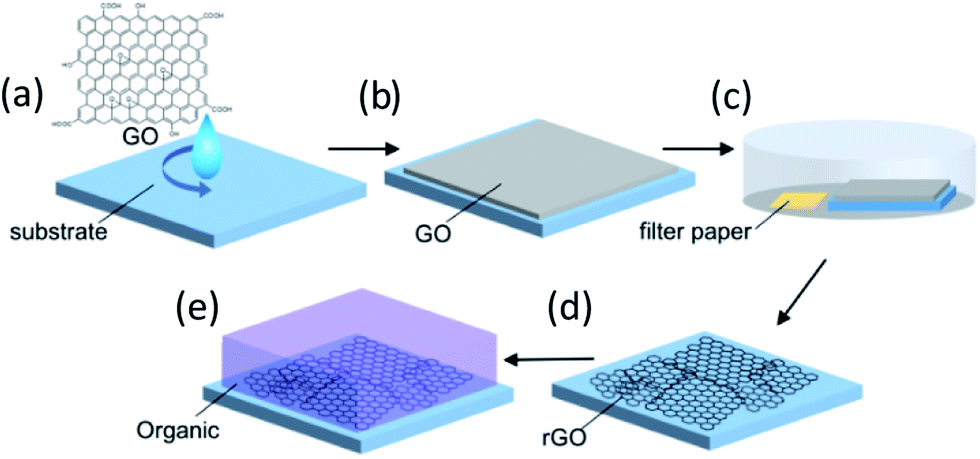 | ||
| Fig. 1 Fabrication of rGO films: (a) spin-coating of the GO aqueous dispersion on the substrates, (b) drying the spin-coated GO film, (c) hydrazine vapor reduction of the GO film with a hydrazine monohydrate-soaked filter paper in a Petri dish, (d) thermal reduction under nitrogen atmosphere, and (e) organic film deposition. | ||
Fig. 2a and b show the atomic force microscopy (AFM) images of GO (before reduction) and rGO (after reduction) on the glass substrate, respectively. The spin-coated, thin GO flakes covered the entire substrate surface without aggregation. The reduction process changed the rGO film morphology, whereby the rGO flake edges became unclear in comparison to the GO film. The root-mean square (RMS) value of the surface roughness decreased from 0.56 nm for GO to 0.27 nm for rGO. The average film thickness of the GO film was estimated by measuring the height of the film edge from the surface of the uncoated substrate (Fig. S1†). The thickness of the GO film was 3.6 nm and decreased to 1.9 nm after reduction. Therefore, the average number of layers of the obtained GO or rGO films was 3–4 because the thickness of a monolayer GO sheet is ∼1 nm.32 These observations indicate that the rGO film had an ultrasmooth surface, and that the decreased spacing between the rGO layers was the result of the detachment of the functional groups. Lateral size distribution and the average diameter of the GO films were analyzed from their AFM images. The average Feret diameter was 4.8 μm and the diameter of ∼50% of all flakes ranged from 2–4 μm (Fig. 3a). The optical transmission spectrum of the rGO film revealed excellent transmittance of 96.9% at 550 nm (Fig. 3b). Considering the high coverage of rGO from the AFM images, this high optical transmittance confirmed the successful formation of an ultrathin rGO film on the substrate.
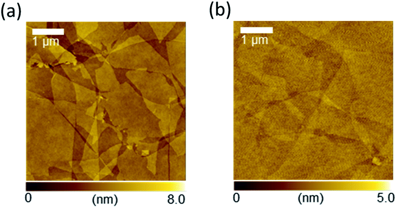 | ||
| Fig. 2 (a and b) Atomic force microscopy (AFM) images of (a) GO and (b) rGO. | ||
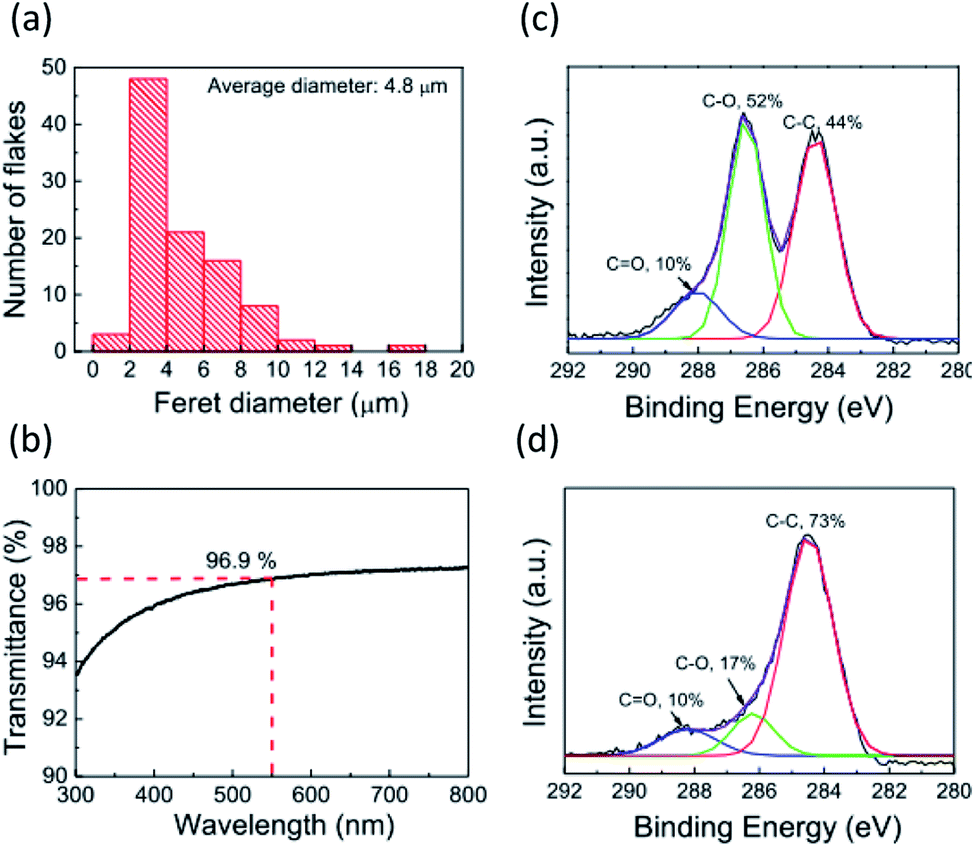 | ||
| Fig. 3 (a) Distribution of Feret diameters of GO flakes. (b) Optical transmission spectrum of the rGO film. (c and d) X-ray photoelectron spectroscopy (XPS) scans of (c) GO and (d) rGO films. | ||
The rGO layer for the template layer is expected to have a good electrical property because it is inserted between the electrode and the organic film. The in-plane electrical conductivities and sheet resistances of the GO and rGO films on the glass substrates were measured (Fig. S2†). The GO film exhibited a high sheet resistance of 3.9 × 10¹¹ Ω sq−1 and a low electrical conductivity of 8.9 × 10⁻⁶ S cm−1, indicating its insulating property. The reduction process drastically improved the electric properties; rGO exhibited a low sheet resistance of 4.6 × 10⁴ Ω sq−1 and a high electrical conductivity of 116 S cm−1. These values are consistent with values reported elsewhere.24,32 The electrical properties are strongly dependent on the chemical state of the rGO film. The C 1s XPS spectrum of the GO film was composed of peaks relating to C![[double bond, length as m-dash]](https://www.rsc.org/images/entities/char_e001.gif) O (∼287.8 eV), C–O (∼286.6 eV), and C–C (284.6 eV) bonds (Fig. 3c). Ratios of the CO, C–O, and C–C bond peaks were 10%, 52%, and 44%, respectively. In the rGO film after the reduction treatment, the ratio of the C–O bond peak decreased to 17%, and the C–C bond ratio increased to 73% (Fig. 3d). Based on the Lerf–Klinowski model that shows a common GO structure, GO has CO bond groups (carbonyl and carboxyl) at the sheet edges and C–O bond groups (ether and hydroxyl) at the basal planes.33 Therefore, the XPS spectra we observe here indicates the detachment of the ether and hydroxyl groups on the GO basal plane, and partial recovery of the π-conjugated planes of GO by the reduction treatment. On the other hand, carbonyl or carboxyl groups likely remained at the sheet edge of the rGO because the CO bond peak ratio did not change. These results from AFM, XPS, and electrical conductivity measurements suggest that the rGO sheet presumably resembled the structure of the graphene sheet, and consequently, could be used as the template layer.
O (∼287.8 eV), C–O (∼286.6 eV), and C–C (284.6 eV) bonds (Fig. 3c). Ratios of the CO, C–O, and C–C bond peaks were 10%, 52%, and 44%, respectively. In the rGO film after the reduction treatment, the ratio of the C–O bond peak decreased to 17%, and the C–C bond ratio increased to 73% (Fig. 3d). Based on the Lerf–Klinowski model that shows a common GO structure, GO has CO bond groups (carbonyl and carboxyl) at the sheet edges and C–O bond groups (ether and hydroxyl) at the basal planes.33 Therefore, the XPS spectra we observe here indicates the detachment of the ether and hydroxyl groups on the GO basal plane, and partial recovery of the π-conjugated planes of GO by the reduction treatment. On the other hand, carbonyl or carboxyl groups likely remained at the sheet edge of the rGO because the CO bond peak ratio did not change. These results from AFM, XPS, and electrical conductivity measurements suggest that the rGO sheet presumably resembled the structure of the graphene sheet, and consequently, could be used as the template layer.
The molecular orientation of the CuPc films on the rGO and normal glass substrates were investigated by X-ray diffraction (XRD) measurements both in out-of-plane and in-plane configurations. The CuPc films were 50 nm, 100 nm, and 300 nm thick. The out-of-plane XRD pattern of the rGO film did not show any diffraction peaks (Fig. S3†). Fig. 4a shows the out-of-plane XRD patterns. CuPc has multiple crystal polymorphs and shows the α phase for room temperature growth. Our XRD patterns were consistent with the crystal structure of α-CuPc having the triclinic slipped-stack structure which was investigated by Hoshino et al.34 The CuPc film on the normal glass substrate showed a distinct diffraction peak at 6.9° assigned to the (100) plane, indicating edge-on molecular orientation. In contrast, the (100) peak on the rGO substrate disappeared, and a distinct (11−2) peak emerged at 27.6° (d = 3.22 Å), thus suggesting face-on orientation (Fig. 4c). The in-plane XRD patterns also supported the change of molecular orientation. The CuPc films on the rGO substrate only show (h00) peaks corresponding to the face-on orientation, whereas those on the glass substrate showed (001) and (01-2) peaks at 7.2° and 26.6°, respectively (Fig. 4b). These in-plane XRD patterns are consistent with the results of the out-of-plane measurements because the former patterns at the face-on orientation should correspond with the latter patterns at the edge-on orientation. The in-plane peaks assigned to the (101) plane also followed this pattern because this plane became vertical to the substrate for the face-on condition. The peaks derived at the face-on orientation (at 27.6° and 6.9° in the out-of- and in-plane configurations, respectively) increased with increasing film thicknesses, indicating that the effect of the rGO under layer was maintained for films with thickness up to 300 nm. The observed XRD patterns of the CuPc film indicating the face-on orientation on rGO corresponds to reported XRD patterns of a CuPc film oriented with CVD graphene.17
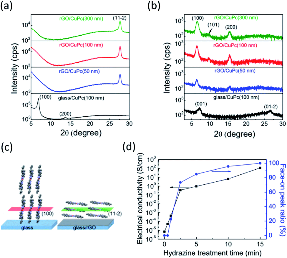 | ||
| Fig. 4 (a and b) X-ray diffraction peak patterns of CuPc in the (a) out-of-plane and (b) in-plane configurations. (c) Molecular orientation of CuPc on glass and rGO. (d) Electrical conductivities of rGO films and peak area ratios of the (11−2) peak showing face-on orientation for different hydrazine treatment times. | ||
The templating effect of rGO is sensitive to its surface condition. To elucidate the effect of reduction, the molecular orientation of the CuPc film on GO was investigated. Here, only the (100) peak assigned to the edge-on orientation was observed (Fig. S4a†), thus indicating that the GO film hardly interacted with the CuPc molecules owing either to the functional groups on the surface or to defected π-conjugated planes. In order to clarify the effect of residual oxygen contents on the templating effect of rGO, we investigated the effects of hydrazine treatment time on peak area ratios of the (11−2) peak of CuPc films and electrical conductivities of the rGO film (Fig. 4d). Electrical conductivities of the rGO films increased with the increase of hydrazine treatment time, indicating the decrease of oxygen content.26 The peak area ratios showed the same tendency, indicating that the molecular orientation changes from edge-on to face-on depending on the oxygen content. The peak area ratio reached 95.6% when the GO film was reduced for 10 minutes. The oxygen content, which can be estimated from the electrical conductivity according to the literature,26 was roughly 30% for that condition. Therefore, the rGO film can work well as the template, even if the oxygen content remains 30%. This result is explained as follows. Defect free graphene areas reportedly cover ∼60% of the rGO sheet and are mixed with defective areas in nanometer order scale.35 It has been also reported that the oxygen content depends on the rGO thickness and the surface is preferentially reduced.36 In that situation, defect free graphene domains would work as starting points of thin-film growth with face-on orientation. First molecules deposited onto the substrate should diffuse onto the surface and form a crystal nucleus due to the interactions with the defect free graphene areas. Molecules coming after that form the face-on orientation by using the firstly oriented molecule as the template.
To confirm the importance of surface smoothness, the molecular orientation on a rough rGO surface prepared via spin-coating a GO dispersion without centrifugation was measured, whereby some fiber structures were observed on the surface and the RMS value was 3.2 nm (Fig. S4b†). Moreover, the XRD patterns of the CuPc film indicate an incomplete face-on orientation with a clear (11−2) peak and weak (100) peak (Fig. S4a†), which suggests that the aggregation of rGO flakes hindered the π–π interactions and diffusion of molecules on the substrate surface. As rGO-flake size affected the molecular orientation and crystal growth, size was optimized by sonicating the GO aqueous dispersion. When CuPc was deposited on an rGO film comprising small-sized flakes with diameter of <1 μm (Fig. S5a†), the XRD pattern indicates an incomplete face-on orientation (Fig. S5b†). This result suggests that the grain boundaries between the rGO flakes and the rough rGO film surface interrupted orientation control. Thus, an ultrasmooth surface with large GO flakes and reduction to rGO are essential for the template layer to control the molecular orientation of organic semiconductors.
The vertical hole mobilities of the CuPc film with and without the rGO template layer were measured using the space-charge-limited current (SCLC) technique. After CuPc deposition, MoO3/Al electrodes were deposited for the hole-only device structure. The CuPc film onto the rGO coated ITO substrate showed the same XRD pattern with that onto the rGO coated glass substrate and the face-on orientation (Fig. S6†). The hole mobilities were estimated using the Mott–Gurney law in eqn (1):
 | (1) |
![[thin space (1/6-em)]](https://www.rsc.org/images/entities/char_2009.gif) J–logVappl plots with 100 nm thickness indicated a slope of 2, which implies that the SCLC was observed for the high-voltage region and thus hole mobility can be estimated from eqn (1). The SCLC hole mobility was enhanced by almost two orders of magnitude from 3.6 × 10⁻⁵ to 1.5 × 10⁻³ cm2 V−1 s−1. This is attributable to the face-on molecular orientation induced by the rGO template layer. The measured vertical hole mobility of the face-on oriented CuPc film is comparable to the horizontal mobility in the edge-on oriented film measured with the field-effect transistor.37 A similar enhancement of electrical properties and hole mobility was previously measured on a single-layer graphene template, which was attributed to an improved orientation of crystallites in the organic film.21 To clarify the relationship between molecular orientation and carrier mobility, the charge transport anisotropy of the CuPc crystal was quantitatively estimated by calculating the electronic couplings for dimer pairs using the Amsterdam Density Functional (ADF) package at the B3LYP/DZP level. The directions for the adjacent molecules are labeled P1, P2, and T1–T4 in the bc plane (Fig. 5b), and L in the ac plane (Fig. 5c). Electronic coupling for the P1 (P2) direction (corresponding to the column axis) has the largest value (22 meV). In contrast, electronic coupling for the other directions (corresponding to the edge-to-edge direction) exhibited small values (2 meV), which are in agreement with the low vertical mobility observed in the edge-on orientation. Thus, the face-on orientation of the CuPc molecules on the rGO substrate was preferable for charge transport owing to the large electronic couplings for the (11−2) direction (π–π stacking direction), thus significantly improving the vertical mobility. The hole mobility of 300 nm thick CuPc films deposited onto the rGO layer was also measured (Fig. S8†). This mobility was measured to be 1.2 × 10⁻² cm2 V−1 s−1 which was almost ten times higher than that of the film with the thickness of 100 nm. In a P3HT film on graphene, an increasing film thickness causes a mixture of crystallites with different orientations (edge-on, face-on and other orientations) producing an interconnected pathway for enhanced charge transport.21 This may also be the case in our study where such an effect might cause the mobility to enhance.
J–logVappl plots with 100 nm thickness indicated a slope of 2, which implies that the SCLC was observed for the high-voltage region and thus hole mobility can be estimated from eqn (1). The SCLC hole mobility was enhanced by almost two orders of magnitude from 3.6 × 10⁻⁵ to 1.5 × 10⁻³ cm2 V−1 s−1. This is attributable to the face-on molecular orientation induced by the rGO template layer. The measured vertical hole mobility of the face-on oriented CuPc film is comparable to the horizontal mobility in the edge-on oriented film measured with the field-effect transistor.37 A similar enhancement of electrical properties and hole mobility was previously measured on a single-layer graphene template, which was attributed to an improved orientation of crystallites in the organic film.21 To clarify the relationship between molecular orientation and carrier mobility, the charge transport anisotropy of the CuPc crystal was quantitatively estimated by calculating the electronic couplings for dimer pairs using the Amsterdam Density Functional (ADF) package at the B3LYP/DZP level. The directions for the adjacent molecules are labeled P1, P2, and T1–T4 in the bc plane (Fig. 5b), and L in the ac plane (Fig. 5c). Electronic coupling for the P1 (P2) direction (corresponding to the column axis) has the largest value (22 meV). In contrast, electronic coupling for the other directions (corresponding to the edge-to-edge direction) exhibited small values (2 meV), which are in agreement with the low vertical mobility observed in the edge-on orientation. Thus, the face-on orientation of the CuPc molecules on the rGO substrate was preferable for charge transport owing to the large electronic couplings for the (11−2) direction (π–π stacking direction), thus significantly improving the vertical mobility. The hole mobility of 300 nm thick CuPc films deposited onto the rGO layer was also measured (Fig. S8†). This mobility was measured to be 1.2 × 10⁻² cm2 V−1 s−1 which was almost ten times higher than that of the film with the thickness of 100 nm. In a P3HT film on graphene, an increasing film thickness causes a mixture of crystallites with different orientations (edge-on, face-on and other orientations) producing an interconnected pathway for enhanced charge transport.21 This may also be the case in our study where such an effect might cause the mobility to enhance.
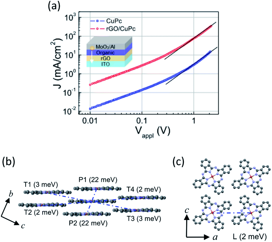 | ||
| Fig. 5 (a) Current density (J)–voltage (Vappl) plots of CuPc films with and without rGO. The CuPc film thickness was 100 nm. (b and c) Single crystal structures of CuPc and charge couplings in the (b) bc plane and (c) ac plane. | ||
Conclusions
In summary, an rGO template layer was prepared by reducing the GO films spin-coated from GO aqueous dispersion to induce the face-on orientation of organic semiconductor molecules. The ultrathin rGO films covered the substrates and showed high optical transparency and high electrical conductivity. The rGO template layer changed the edge-on molecular orientation of CuPc to the face-on orientation and improved its vertical hole mobility by almost two orders of magnitude owing to the preferable π–π stacking in the vertical direction. This efficient and easily fabricated template layer helps solving the vertical mobility problem and can potentially improve the performances of various vertical devices, including OLEDs, organic photovoltaic devices, and vertical organic transistors.Experimental section
Preparation of rGO films
GO aqueous dispersion (4 mg mL−1) was purchased from Sigma-Aldrich. The GO aqueous dispersion (1 mL, 1 mg mL−1) was centrifuged at 5000 rpm (1957g) for 15 min. The supernatant was collected and centrifuged at 3000 rpm (704g) for 30 min. This step was repeated 5 times. The supernatant was then centrifuged at 10000 rpm (7826g) for 30 min. The precipitate was finally redispersed in 1 mL of pure water and centrifuged at 10000 rpm for 60 min. The precipitate was collected and used for film fabrication. Concentration of the final purified product was ∼1 mg mL−1. Glass and ITO substrates, 20 × 25 mm squares were cleaned by rubbing with acetone soaked wipes, and sonicating in acetone and isopropanol for 10 min. The washed substrates were treated with a UV-O3 cleaner (Filgen, UV253V8). O2 gas was flown into the cleaner chamber at 0.1 MPa for 2 min, followed by UV-light irradiation onto the substrates for 20 min, and then N2 gas was flown into the chamber for 2 min. The water contact angle of the glass substrate changed from 37.5 degree to 3.6 degree by the UV-O3 treatment. 300 μL of the centrifuged GO aqueous dispersion was dropped on the substrates and spin-coated. In order to fabricate the uniform GO film and evaporate water, rotational speed was gradually accelerated. The substrates were rotated at 500 rpm for 120 s, then at 1000 rpm for 30 s, and at 2000 rpm for 30 s. The spin-coated GO films were then dried on a hot plate at 100 °C for 10 min in air. The GO films on the substrates were placed in a cleaned glass Petri dish, 120 mm diameter and 20 mm height with a filter paper containing 300 μL of hydrazine monohydrate for hydrazine vapor reduction. The dish was covered with another larger Petri dish and heated on a hot plate at 90 °C for 15 min in air. The GO films after hydrazine vapor reduction were heated at 300 °C for 6 h under a nitrogen atmosphere.
Organic film deposition and hole-only device fabrication
CuPc purified by sublimation was purchased from Lumtec and purified by sublimation before the thin film fabrication. The hole-only device structure was glass/ITO/rGO, none/CuPc (100 nm)/MoO3 (10 nm)/Al (100 nm). CuPc, MoO3, and Al were deposited by thermal vacuum evaporation through a shadow mask under a pressure of ∼10−4 Pa. The deposition rate of CuPc was 1 Å s−1.Analysis of rGO and CuPc films
The film surface morphologies were observed by an AFM (SII, SPA-400) with a DFM mode. The thin-film crystal structure was investigated by an X-ray diffractometer (Rigaku, SmartLab) with out-of-plane and in-plane configurations and Cu Kα radiation (λ = 1.5418 Å). The current–voltage properties were measured with a semiconductor parameter analyzer (Agilent, 4155C) in a nitrogen-filled glove box. The XPS spectra were measured by Shimadzu, KRATOS AXIS-165x with monochromated Al Kα radiation (hν = 1486.6 eV).Conflicts of interest
There are no conflicts of interest to declare.Acknowledgements
This research was supported by the Grants-in-Aid for Scientific Research (KAKENHI, JP17H03134) from the Japan Society for the Promotion of Science (JSPS). The authors wish to acknowledge Prof. A. Saeki from Osaka University for the photoelectron yield spectroscopy (PYS) measurement.References
- J. E. Anthony, J. S. Brooks, D. L. Eaton and S. R. Parkin, J. Am. Chem. Soc., 2001, 123, 9482–9483 CrossRef CAS.
- Y. Yuan, G. Giri, A. L. Ayzner, A. P. Zoombelt, S. C. B. Mannsfeld, J. Chen, D. Nordlund, M. F. Toney, J. Huang and Z. Bao, Nat. Commun., 2014, 5, 3005 CrossRef.
- K. Yamada, Y. Suwa, C. Katagiri and K.-i. Nakayama, Org. Electron., 2018, 53, 320–324 CrossRef CAS.
- A. Hinderhofer, U. Heinemeyer, A. Gerlach, S. Kowarik, R. M. J. Jacobs, Y. Sakamoto, T. Suzuki and F. Schreiber, J. Chem. Phys., 2007, 127, 194705 CrossRef.
- D. Yokoyama, J. Mater. Chem., 2011, 21, 19187–19202 RSC.
- I. Osaka, M. Saito, T. Koganezawa and K. Takimiya, Adv. Mater., 2014, 26, 331–338 CrossRef CAS.
- T. Minakata, H. Imai, M. Ozaki and K. Saco, J. Appl. Phys., 1992, 72, 5220–5225 CrossRef CAS.
- R. Ruiz, D. Choudhary, B. Nickel, T. Toccoli, K.-C. Chang, A. C. Mayer, P. Clancy, J. M. Blakely, R. L. Headrick, S. Iannotta and G. G. Malliaras, Chem. Mater., 2004, 16, 4497–4508 CrossRef CAS.
- S. B. Jo, H. H. Kim, H. Lee, B. Kang, S. Lee, M. Sim, M. Kim, W. H. Lee and K. Cho, ACS Nano, 2015, 9, 8206–8219 CrossRef CAS.
- N. N. Nguyen, S. B. Jo, S. K. Lee, D. H. Sin, B. Kang, H. H. Kim, H. Lee and K. Cho, Nano Lett., 2015, 15, 2474–2484 CrossRef CAS.
- S. Heutz, G. Salvan, T. S. Jones and D. R. T. Zahn, Adv. Mater., 2003, 15, 1109–1112 CrossRef CAS.
- C. H. Cheng, J. Wang, G. T. Du, S. H. Shi, Z. J. Du, Z. Q. Fan, J. M. Bian and M. S. Wang, Appl. Phys. Lett., 2010, 97, 083305 CrossRef.
- C. Schünemann, D. Wynands, K.-J. Eichhorn, M. Stamm, K. Leo and M. Riede, J. Phys. Chem. C, 2013, 117, 11600–11609 CrossRef.
- L. A. Rochford, D. S. Keeble, O. J. Holmes, G. J. Clarkson and T. S. Jones, J. Mater. Chem. C, 2014, 2, 6056–6060 RSC.
- T. Taima, M. Shahiduzzaman, T. Ishizeki, K. Yamamoto, M. Karakawa, T. Kuwabara and K. Takahashi, J. Phys. Chem. C, 2017, 121, 19699–19704 CrossRef CAS.
- K. Yamada and K. Nakayama, J. Electrochem. Soc., 2019, 166, B3103–B3108 CrossRef CAS.
- K. Xiao, W. Deng, J. K. Keum, M. Yoon, I. V. Vlassiouk, K. W. Clark, A.-P. Li, I. I. Kravchenko, G. Gu, E. A. Payzant, B. G. Sumpter, S. C. Smith, J. F. Browning and D. B. Geohegan, J. Am. Chem. Soc., 2013, 135, 3680–3687 CrossRef CAS.
- J. M. Mativetsky, H. Wang, S. S. Lee, L. Whittaker-Brooks and Y. L. Loo, Chem. Commun., 2014, 50, 5319–5321 RSC.
- L. Zhang, S. S. Roy, N. S. Safron, M. J. Shearer, R. M. Jacobberger, V. Saraswat, R. J. Hamers, M. S. Arnold and T. L. Andrew, Adv. Mater. Interfaces, 2016, 3, 1600621 CrossRef.
- B.-Y. Shi and W.-D. Dou, Thin Solid Films, 2017, 636, 723–729 CrossRef CAS.
- V. Skrypnychuk, N. Boulanger, V. Yu, M. Hilke, S. C. B. Mannsfeld, M. F. Toney and D. R. Barbero, Adv. Funct. Mater., 2015, 25, 664–670 CrossRef CAS.
- V. Skrypnychuk, N. Boulanger, V. Yu, M. Hilke, M. F. Toney and D. R. Barbero, J. Mater. Chem. C, 2016, 4, 4143–4149 RSC.
- W. H. Lee, J. Park, S. H. Sim, S. Lim, K. S. Kim, B. H. Hong and K. Cho, J. Am. Chem. Soc., 2011, 133, 4447–4454 CrossRef CAS.
- H. A. Becerril, J. Mao, Z. Liu, R. M. Stoltenberg, Z. Bao and Y. Chen, ACS Nano, 2008, 2, 463–470 CrossRef CAS.
- C. Mattevi, G. Eda, S. Agnoli, S. Miller, K. A. Mkhoyan, O. Celik, D. Mastrogiovanni, G. Granozzi, E. Garfunkel and M. Chhowalla, Adv. Funct. Mater., 2009, 19, 2577–2583 CrossRef CAS.
- N. Morimoto, T. Kubo and Y. Nishina, Sci. Rep., 2016, 6, 21715 CrossRef CAS.
- S.-S. Li, K.-H. Tu, C.-C. Lin, C.-W. Chen and M. Chhowalla, ACS Nano, 2010, 4, 3169–3174 CrossRef CAS.
- X. Wang, L. Zhi and K. Müllen, Nano Lett., 2008, 8, 323–327 CrossRef CAS PubMed.
- J. M. Yun, J. S. Yeo, J. Kim, H. G. Jeong, D. Y. Kim, Y. J. Noh, S. S. Kim, B. C. Ku and S. I. Na, Adv. Mater., 2011, 23, 4923–4928 CrossRef CAS.
- T. A. Amollo, G. T. Mola and V. O. Nyamori, Sol. Energy, 2018, 171, 83–91 CrossRef CAS.
- G. Eda and M. Chhowalla, Adv. Mater., 2010, 22, 2392–2415 CrossRef CAS.
- S. Stankovich, D. A. Dikin, R. D. Piner, K. A. Kohlhaas, A. Kleinhammes, Y. Jia, Y. Wu, S. T. Nguyen and R. S. Ruoff, Carbon, 2007, 45, 1558–1565 CrossRef CAS.
- A. Lerf, H. He, M. Forster and J. Klinowski, J. Phys. Chem. B, 1998, 102, 4477–4482 CrossRef CAS.
- A. Hoshino, Y. Takenaka and H. Miyaji, Acta Crystallogr., Sect. B: Struct. Sci., 2003, 59, 393–403 CrossRef.
- C. Gómez-Navarro, J. C. Meyer, R. S. Sundaram, A. Chuvilin, S. Kurasch, M. Burghard, K. Kern and U. Kaiser, Nano Lett., 2010, 10, 1144–1148 CrossRef.
- L. Sygellou, G. Paterakis, C. Galiotis and D. Tasis, J. Phys. Chem. C, 2016, 120, 281–290 CrossRef CAS.
- Z. Bao, A. J. Lovinger and A. Dodabalapur, Appl. Phys. Lett., 1996, 69, 3066–3068 CrossRef CAS.
Footnote |
| † Electronic supplementary information (ESI) available: Experimental details and additional data. See DOI: 10.1039/c9ra06258k |
| This journal is © The Royal Society of Chemistry 2019 |