
 Open Access Article
 This Open Access Article is licensed under a Creative Commons Attribution-Non Commercial 3.0 Unported Licence
Intermediate band solar cell materials through the doping of group-VA elements (N, P, As and Sb) in Cu2ZnSiSe4
Muhammad Jibrana,
Xia Sun *ab,
Bing Wanga,
Yasushi Yamauchib and
Zejun Dinga
*ab,
Bing Wanga,
Yasushi Yamauchib and
Zejun Dinga
aHefei National Laboratory for Physical Sciences at the Microscale, Department of Physics, University of Science and Technology of China, 96 Jinzhai Road, Hefei, Anhui 230026, China. E-mail: sunx@ustc.edu.cn
bNational Institute for Materials Science, 1-2-1 Sengen, Tsukuba, Ibaraki 305-0047, Japan
First published on 9th September 2019
Abstract
The electronic structure and optical properties of group-VA (N, P, As, and Sb)-doped Cu2ZnSiSe4 alloys have been studied using a hybrid functional through density functional theory calculations. The minor lattice distortion and small formation energy indicate that synthesis of these alloys is highly possible in experiment. For each doped alloy, an isolated and partially filled intermediate band (IB) appears in its band structure. The doping-induced IB is mainly contributed by the s states of the doped group-VA atom and the p states of four neighboring Se atoms, and slightly by the d states of eight Cu atoms. The existence of an IB obviously enhances the absorption coefficient with two additional absorption peaks in the visible light range. For P, As and Sb-doped Cu2ZnSiSe4 alloys, not only the bandgap between the valence band maximum and the conduction band minimum but also the sub bandgap between the valence band maximum and the IB are very close to the optimal values for visible light absorption. Therefore, these alloys are recommended as good candidates for IB solar cell materials.
1. Introduction
Intermediate band (IB) materials have attracted great attention due to their promising ability to enhance the efficiency of solar cells.1,3–11 The IB locates between the valence band maximum (VBM) and the conduction band minimum (CBM). To achieve high photocurrent and photo-voltage, the IB should be isolated and partially filled. Therefore, electrons can be excited not only from the VB to the CB, but also from the VB to the IB and from the IB to the CB. The detailed balance efficiency limit of IB solar cells (IBSCs) (63.1%)1 is greatly higher than that of ordinary single-junction solar cells (30%).2Many investigations have been carried to fabricate various kinds of IBSCs.3–11 First typical IBSC is designed and manufactured using quantum dot (QD) technology.3,4 Photocurrent produced by the electron transition from IB to CB is experimentally measured.3 However, the IBSCs fabricated by QD technology have low density of states (DOS) in the IB and small bandgap in the host material (such as 1.42 eV for GaAs). Both of the factors substantially limit the enhancement of their efficiency. It is reported that the optimal bandgap for IBSCs at 1 sun is 2.41 eV with IB locating at 0.92 eV from the CB or the VB.5 Chalcopyrite CuGaS2 is regarded as an excellent host for IBSCs due to its appropriate bandgap (2.43 eV).12 The IBs are predicted to be formed by doping of 3d-metal atoms such as Ti,11,13 Cr,10,11 Fe,8,14 and Ni8 in CuGaS2. The shortcomings of the IBs induced by doping of Ti, Fe and Ni in CuGaS2 are occupied or unoccupied based on relatively accurate hybrid functionals,8,15 but not partially filled states which are expected in practical applications. Furthermore, Yang et al. proposed that transition metals might not be the best dopant to fabricate IBSCs.16 The localized 3d states of transition metals may result in low light absorption coefficient and low carrier mobility.16 Elements from group-IV and VA as dopants create delocalized s states which could be more appropriate to enhance the parameters.16–19 For the host of Cu2ZnSnS4, the doping of Sb at Sn site has the lowest formation energy than other sites such as Cu, Zn and S.17 By using more accurate hybrid functional instead of the generalized gradient approximation (GGA), it is predicted that partially filled IBs can form in Sn-doped CuInS2 and CuGaS2,16 (P, As, Sb)-codoped CuGaS2 at Ga and S sites,19 (Si, Ge, Sn)-doped AgAlTe2,18 and Sb-doped Cu2ZnSnS4.17 Whereas, the use of toxic or costly elements, like Ga, Ag, Te or In, in the host materials is highly demanded to be replaced by nontoxic and cheap elements.
In this paper, the Cu2ZnSiSe4 alloy is chosen as host material, whose bandgap (2.33 eV)20 is very close to the ideal value (2.41 eV) for IBSCs.5 The group-VA elements (N, P, As, and Sb) are selected as dopants to replace Si atom in order to easily form n-type semiconductor. The delocalized s states of group-VA elements will help to form delocalized IBs and generate freely transported carriers. Our calculation shows that an isolated and partially filled IB is induced in all the four doped alloys. The IB is dominated by the hybridization of M-s and Se-p states as well as slightly contributed by Cu-d states. Compared with that of the host material, absorption coefficient of group-VA doped Cu2ZnSiSe4 is largely enhanced with additional two peaks in the visible light range.
2. Computational details
All calculations are performed with in the density functional theory (DFT) using Vienna Ab initio Simulation Package (VASP)21,22 with the projector augmented wave (PAW) method.23 The plane-wave energy cutoff is set to 400 eV. Our previous study has revealed that the total energy of Cu2ZnSiSe4 in kesterite (KS) structure (Fig. 1a) is lower than those in stannite and wurtzite-stannite structures through both GGA and hybrid functional calculations.24 Experimentally, Cu2ZnSiSe4 and Cu2ZnSiS4 are observed in wurtzite-stannite structure25,26 but Cu2ZnGeSe4 in KS structure.27 Here, a 2 × 2 × 1 supercell of KS structure is used which includes 64 atoms. One Si atom is replaced by one group-VA atom M (M = N, P, As and Sb) in this supercell. Correspondingly, the dopant concentration is 12.5%. A 4 × 4 × 4 k-point mesh is applied using Monkhorst–Pack method in all calculations.28 Structural optimizations are performed by GGA with the Perdew–Burke–Ernzerhof (PBE) form.29 The band structure and optical property are calculated through hybrid functional, which is known to be more accurate than GGA in prediction of electronic property of semiconductors. However, the calculated bandgap of Cu2ZnSiSe4 is 1.76 eV through standard HSE06,30 which is obviously still smaller than the experimental value (2.33 eV).20 The bandgap depends on the mixing parameter α, which defines the fraction of exact exchange and is set as 0.25 in HSE06.30 When the value of α is adjusted to 0.35, the corresponding bandgap is increased to 2.26 eV, which is much closer to the experimental value. The adjustment of α is also adopted in the calculation of Cu2ZnSnS4 (ref. 17) and Cu2CdxZn1−xSnS4.31 In this study, all calculations have used an increased α value (0.35).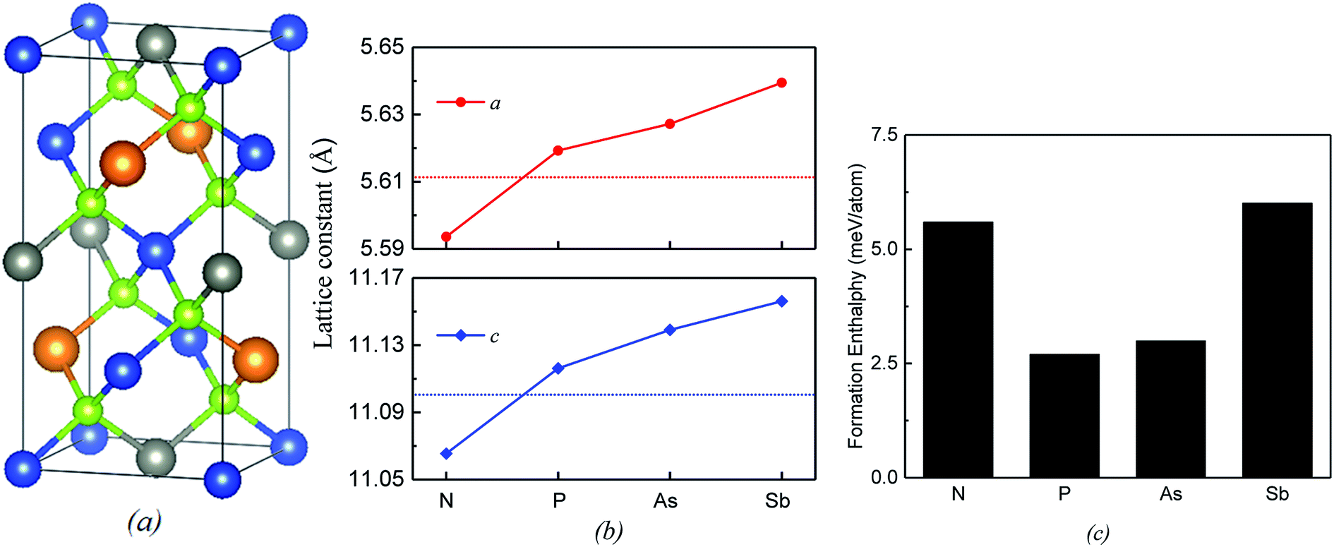 | ||
| Fig. 1 (a) Crystal structure of Cu2ZnSiSe4 in kesterite (KS) phase. The Cu, Zn, Si, and Se atoms are represented by blue, grey, orange and green spheres, respectively. (b) The calculated lattice constants. (c) Formation enthalpy of group-VA doped Cu2ZnSi0.875M0.125Se4 (M = N, P, As and Sb) alloys. | ||
3. Results and discussion
Our calculations show that the lattice constants (a and c) decrease in the presence of the N substitution and increase in the presence of the P, As and Sb substitutions (Fig. 1a and b). For the P-doped alloy, the lattice variation is only 0.16% due to atomic radii of the doped P element close to the one of Si element. Even for the elements with larger atomic number (As, Sb), the lattice variations are less than 0.6%, indicating that the lattice distortion is minor. Such minor lattice distortion is quite favorable to the synthesis of doped alloys. Actually, primary change occurs at the local geometry around dopant. The bond length of Si–Se in the host Cu2ZnSiSe4 is 2.337 Å. After the substitution of one Si atom by one group-VA atom M, the bond lengths of M-Se (M = N, P, As and Sb) are 2.199, 2.438, 2.543 and 2.683 Å, respectively. In accordance with atomic radii, the variation is smallest by the doping of P and largest by that of Sb. To evaluate the miscibility of group-VA doped Cu2ZnSiSe4 alloys, the formation enthalpy ΔH(M) is defined and calculated as:| ΔH(M) = ECu2ZnSi0.875M0.125Se4 − 0.875ECu2ZnSiSe4 − 0.125ECu2ZnMSe4 |
Band structures of the host and doped alloys are shown in Fig. 2a. The calculated bandgap of Cu2ZnSiSe4 (2.26 eV) agrees well with the experimental value (2.33 eV).20 Energy interval of 0.40 eV between the VBM and the Fermi level (EF) is smaller than that value of 1.86 eV between the EF and the CBM. After the doping of group-VA atom M (M = N, P, As and Sb), the bandgaps between CBM and VBM (ΔCBM–VBM) are among 2.21–2.39 eV, close to that of host (Fig. 2b). The most significant variation in band structure is the introduction of IB. For all the four doped cases, IBs are isolated and partially filled. This is exactly what IBSCs need to ensure the three-photon absorption processes. As indicated in Fig. 2a, IBs introduced by these four dopants have similar shapes, but positions of the band edges (CBM and VBM) show dependence on the specific dopants. Fig. 2b shows the bandgap and two sub bandgaps of doped alloys, one is between the CBM and IB at the Γ point (Δ1 CBM–IB) and the other is between the IB and VBM at the Γ point(Δ2 IB–VBM). It is noticed that shapes of the edges of VBM and CBM have no big difference among four doped alloys. The N-doped alloy has the largest Δ1 CBM–IB(2.09 eV) and the smallest Δ2 IB–VBM (0.29 eV). In contrast, the P-doped alloy has the smallest Δ1 CBM–IB (1.30 eV) and the largest Δ2 IB–VBM (1.00 eV), which will be discussed later.
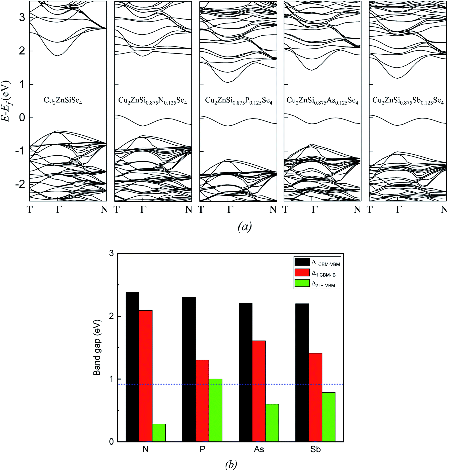 | ||
| Fig. 2 (a) The band structures of host material (Cu2ZnSiSe4) and group-VA doped alloys Cu2ZnSi0.875M0.125Se4 (M = N, P, As and Sb). Fermi level of each alloy is set to zero (b) the bandgap between CBM and VBM, and two sub bandgaps between CBM and IB, IB and VBM, respectively. The dotted line represents the optimal value of sub bandgap for IBSCs. | ||
Fig. 3a and b show the total DOS and projected DOS (PDOS) of group-VA doped Cu2ZnSiSe4 alloys. The VBM are mainly composed by Cu-3d and Se-4p states (Fig. 3b), same as the host material. As to the conduction band, a prominent peak locates at about 2.0 eV. Beside the Se-4p and Si-3s states, there is obvious contribution from the p states of doped elements M (M = N, P, As and Sb) to this peak. Fig. 3c plots the isosurface of the band-decomposed charge density of IB for the P-doped alloy. IB charge density is contributed dominantly by one doping atom (P) and four neighboring Se atoms, as well as slightly by eight adjacent Cu atoms in the supercell. Similarly, the IBs of other three doped alloys are also primarily composed by the anti-bonding states of M-s and Se-4p. The atomic orbital energies of N-2s, P-3s, As-4s and Sb-5s are −18.58, −13.97, −14.49 and −12.83 eV, respectively. Since the atomic orbital energy of N-2s is much lower than the other three, the corresponding IB formed by the anti-bonding hybridization of N-2s and Se-4p is at the lowest position and closest to the VBM, resulting in the smallest Δ2 IB–VBM. Besides the atomic orbital energy, interactions between doped elements and Se atoms are influenced by their bond lengths. Although atomic orbital energy of P-3s (−13.97 eV) is lower than that of Sb-5s (−12.83 eV), the bond length of P–Se (2.438 Å) is smaller than that of As–Se (2.683 Å). The anti-bonding state by P-3s and Se-4p is pushed to a higher energy than that by Sb-4s and Se-4p. Therefore, the IB of P-doped alloy stays at the highest position among four anti-bonding states and has the largest value of Δ2 IB–VBM, as indicated in Fig. 2b.
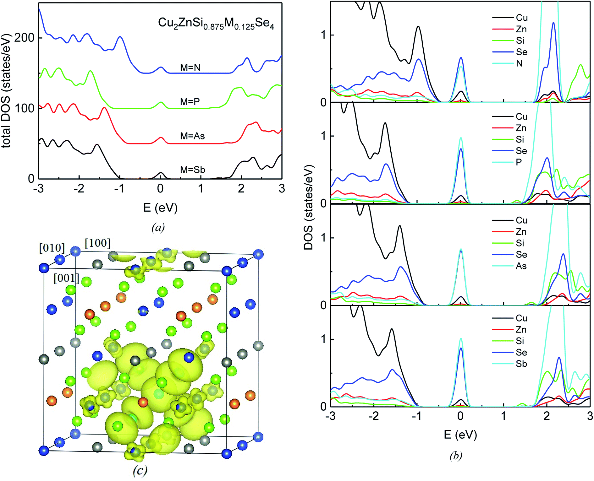 | ||
| Fig. 3 (a) Total DOS and (b) PDOS of Cu, Zn, Si, Se and M (M = N, P, As, Sb) of group-VA doped Cu2ZnSi0.875M0.125Se4. (c) Partial charge density of the intermediate band (IB) of Cu2ZnSi0.875P0.125Se4. The iso-surface is plotted with 0.0015 e Å−3. The blue, grey, orange, green and cyan spheres represent Cu, Zn, Si, Se and P atoms, respectively. | ||
Fig. 4 compares optical absorption coefficients α(ω) of group-VA doped alloys with that of the host material. Solar spectrum is also shown in the background. It can be seen that the difference of α(ω) in the zz and xx directions (parallel to the c and a axis, respectively) is insignificant. For the host of Cu2ZnSiSe4 (blue lines in Fig. 4), there is only one absorption peak (2.62 eV) at the main solar light energy range, which corresponds to the electron transition from the VB to the CB. Furthermore, absorption coefficient is considerably small when the photon energy is below 2.0 eV. It is noticed that there are three absorption peaks (labeled as I, II, and III, respectively, in Fig. 4) for each doped alloy. The peak I, caused by electron transition from VB to CB, slightly shifts to higher energy for the doping of N and P but shifts to lower energy for the doping of Sb. This is due to the bandgap between the VBM and CBM slightly increases for the doping of N and P and decreases for the doping of Sb. The additional two peaks (II and III), caused by electron transitions from the IB to CB and from the VB to IB, locate at lower energy with more intensity of the solar light. Therefore, the absorption energy range is substantially broadened and the absorption coefficient is greatly enhanced due to dopant-introduced IBs. It is worth noticing that except N-doped alloy, the sub bandgaps Δ2 IB–VBM of P, As and Sb-doped alloys (1.00, 0.64 and 0.80 eV, respectively) are very close to the optimal value (0.92 eV), indicating that these doped alloys are promising candidates for the IBSC materials.
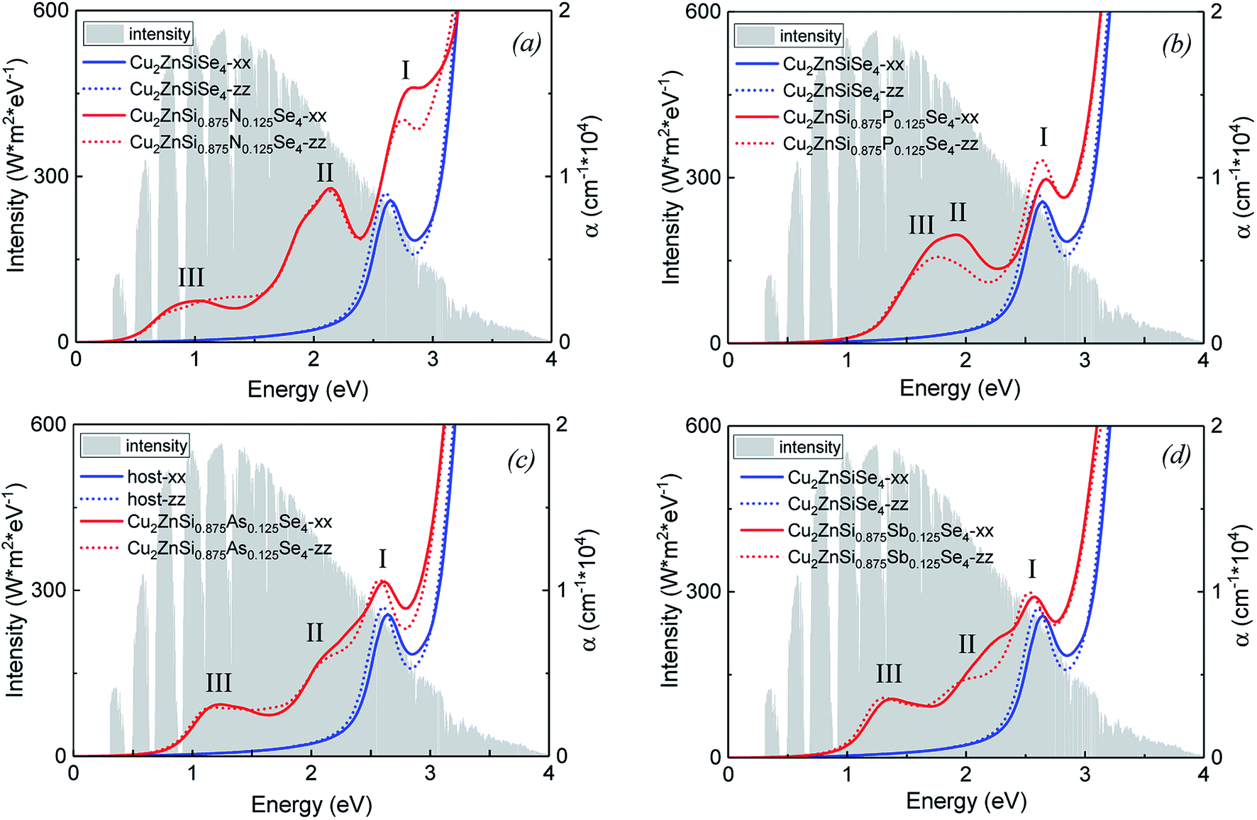 | ||
| Fig. 4 The absorption coefficients of group-VA doped and host alloys. The solid and dotted lines represent the absorption coefficients parallel to the a-axis (αxx) and c-axis (αzz), respectively. The intensity of the solar light spectrum is also shown as a background. (a) M = N, (b) M = P, (c) M = As, (d) M = Sb. M is the doped group-VA atom. | ||
4. Conclusions
We have investigated electronic and optical properties of the group-VA (N, P, As, and Sb)-doped Cu2ZnSiSe4 alloys through hybrid functional calculations. The band structure predicted with an adjusted mixing parameter α (0.35) is more accurate than that through standard HSE06 functional. An isolated and partial filled IB is introduced by the doping of group-VA elements. IBs are formed dominantly by the anti-bonding hybridization of doped M-s states (M = N, P, As and Sb) and Se-4p states. For all of the four doped alloys, three absorption peaks can be clearly observed in the spectra and corresponding to the electron transitions from the VB to CB, IB to CB and VB to IB, respectively. The absorption energy range is substantially broadened and the absorption coefficient is greatly enhanced. This result indicates that group-VA doped Cu2ZnSiSe4 alloys are promising intermediate band solar cell materials with high absorption efficiency for solar energy.Conflicts of interest
There are no conflicts of interest to declare.Acknowledgements
This work was supported by the National Natural Science Foundation of China under Grant Nos. 11674297, 11574289, U1632273 and Anhui Initiative in Quantum Information Technologies (AHY090300).References
- A. Luque and A. Martí, Increasing the efficiency of ideal solar cells by photon induced transitions at intermediate levels, Phys. Rev. Lett., 1997, 78, 5014–5017 CrossRef CAS.
- W. Shockley and H. Queisser, Detailed Balance Limit of Efficiency of p-n Junction Solar Cells, J. Appl. Phys., 1960, 1640, 510–519 Search PubMed.
- A. Martí, E. Antolín, C. R. Stanley, C. D. Farmer, N. López, P. Díaz, E. Cánovas, P. G. Linares and A. Luque, Production of photocurrent due to intermediate-to-conduction-band transitions: A demonstration of a key operating principle of the intermediate-band solar cell, Phys. Rev. Lett., 2006, 97, 247701 CrossRef PubMed.
- S. Tomić, Intermediate-band solar cells: Influence of band formation on dynamical processes in InAs/GaAs quantum dot arrays, Phys. Rev. B: Condens. Matter Mater. Phys., 2010, 82, 195321 CrossRef.
- A. Martí, D. F. Marrón and A. Luque, Evaluation of the efficiency potential of intermediate band solar cells based on thin-film chalcopyrite materials, J. Appl. Phys., 2008, 103, 073706 CrossRef.
- T. Tanaka, M. Miyabara, Y. Nagao, K. Saito, Q. Guo, M. Nishio, K. M. Yu and W. Walukiewicz, Photocurrent induced by two-photon excitation in ZnTeO intermediate band solar cells, Appl. Phys. Lett., 2013, 102, 052111 CrossRef.
- I. Aguilera, P. Palacios and P. Wahnón, Optical properties of chalcopyrite-type intermediate transition metal band materials from first principles, Thin Solid Films, 2008, 516, 7055 CrossRef CAS.
- M. Han, X. Zhang and Z. Zeng, The investigation of transition metal doped CuGaS2 for promising intermediate band materials, RSC Adv., 2014, 4, 62380–62386 RSC.
- P. Palacios, I. Aguilera, K. Sánchez, J. C. Conesa and P. Wahnón, Transition-metal-substituted indium thiospinels as novel intermediate-band materials: prediction and understanding of their electronic properties, Phys. Rev. Lett., 2008, 101, 046403 CrossRef CAS PubMed.
- P. Chen, M. Qin, H. Chen, C. Yang, Y. Wang and F. Huang, Cr incorporation in CuGaS2 chalcopyrite: a new intermediate-band photovoltaic material with wide-spectrum solar absorption, Phys. Status Solidi A, 2013, 210, 1098 CrossRef CAS.
- I. Aguilera, P. Palacios and P. Wahnón, Enhancement of optical absorption in Ga-chalcopyrite-based intermediate-band materials for high efficiency solar cells, Sol. Energy Mater. Sol. Cells, 2010, 94, 1903 CrossRef CAS.
- Ternary chalcopyrite semiconductors: growth electronic properties and applications, ed. J. L. Shay, J. H. Wernick and B. R. Pamplin, Pergamon Press, Oxford, New York, 1st edn, 1975, pp. 110–128 Search PubMed.
- X. Lv, S. Yang, M. Li, H. Li, J. Yi, M. Wang, G. Niu and J. Zhong, Investigation of a novel intermediate band photovoltaic material with wide spectrum solar absorption based on Ti-substituted CuGaS2, Sol. Energy, 2014, 103, 480–487 CrossRef CAS.
- B. Marsen, S. Klemz, T. Unold and H. W. Schock, Investigation of the sub-bandgap photoresponse in CuGaS2: Fe for intermediate band solar cells, Prog. Photovolt. Res. Appl., 2012, 20, 625–629 CrossRef CAS.
- J. Hashemi, A. Akbari, S. Huotari and M. Hakala, Multi-intermediate-band character of Ti-substituted CuGaS2: implications for photovoltaic applications, Phys. Rev. B: Condens. Matter Mater. Phys., 2014, 90, 075154 CrossRef.
- C. Yang, M. Qin, Y. Wang, D. Wan, F. Huang and J. Lin, Observation of an intermediate band in Sn-doped chalcopyrites with wide-spectrum solar response, Sci. Rep., 2013, 3, 1286 CrossRef PubMed.
- X. Zhang, M. Han, Z. Zeng and Y. Duan, The role of Sb in solar cell material Cu2ZnSnS4, J. Mater. Chem. A., 2017, 5, 6606–6612 RSC.
- D. Huang, J.-W. Jiang, J. Guo, Y.-J. Zhao, R. Chen and C. Persson, Group-IV (Si, Ge, and Sn)-doped AgAlTe2 for intermediate band solar cell from first principles study, Semicond. Sci. Technol., 2017, 32, 065007 CrossRef.
- M. Han, X. Zhang, Y. Zhang and Z. Zeng, The group VA element non-compensated n-p codoping in CuGaS2 for intermediate band materials, Sol. Energy Mater. Sol. Cells, 2016, 144, 664–670 CrossRef CAS.
- H. Matsushita, T. Ichikawa and a Katsui, Structural, thermodynamical and optical properties of Cu2-II-IV-VI4 quaternary compounds, J. Mater. Sci., 2005, 40, 2003–2005 CrossRef CAS.
- G. Kresse and J. Furthmüller, Efficiency of ab-initio total energy calculations for metals and semiconductors using a plane-wave basis set, Comput. Mater. Sci., 1996, 6, 15–50 CrossRef CAS.
- G. Kresse and J. Furthmüller, Efficient iterative schemes for ab initio total-energy calculations using a plane-wave basis set, Phys. Rev. B: Condens. Matter Mater. Phys., 1996, 54, 11169–11186 CrossRef CAS PubMed.
- P. E. Blochl, Projector augmentead-wave method, Phys. Rev. B, 1994, 50, 17953 CrossRef PubMed.
- M. Jibran, Z. Y. Li, X. Sun, B. Wang, Y. Yamauchi and Z. J. Ding, Structural, electronic and optical properties of bandgap-tunable Cu2ZnSixSn1-xSe4 alloys, Chem. Phys. Lett., 2018, 705, 92–96 CrossRef CAS.
- A. P. Litvinchuk, V. M. Dzhagan, V. O. Yukhymchuk, M. Ya. Valakh, O. V. Parasyuk, L. V. Piskach, X. Wang, A. J. Jacobson and D. R. T. Zahn, Crystal structure and vibrational properties of Cu2ZnSiSe4 quaternary semiconductor, Phys. Status Solidi B, 2016, 253, 1808–1815 CrossRef CAS.
- M. Guc, S. Levcenko, V. Izquierdo-Roca, X. Fontane, M. Ya. Valakh, E. Arushanov and A. Pérez-Rodríguez, Polarized Raman scattering analysis of Cu2ZnSiS4 and Cu2ZnSiSe4 single crystals, J. Appl. Phys., 2013, 114, 173507 CrossRef.
- M. Ya. Valakh, A. P. Litvinchuk, V. M. Dzhagan, V. O. Yukhymchuk, A. M. Yaremko, Yu. A. Romanyuk, M. Guc, I. V. Bodnar, A. Pérez-Rodríguez and D. R. T. Zahn, Fermi resonance in the phonon spectra of quaternary chalcogenides of the type Cu2ZnGeS4, J. Phys.: Condens. Matter, 2016, 28, 065401 CrossRef PubMed.
- H. J. Monkhorst and J. D. Pack, Special points for Brillouin-zone integrations, Phys. Rev. B: Solid State, 1976, 13, 5188–5192 CrossRef.
- J. P. Perdew, K. Burke and M. Ernzerhof, Generalized gradient approximation made simple, Phys. Rev. Lett., 1996, 77, 3865–3868 CrossRef CAS PubMed.
- J. Heyd, G. E. Scuseria, M. Ernzerhof, J. Heyd, G. E. Scuseria and M. Ernzerhof, Hybrid functionals based on a screened Coulomb potential hybrid functionals based on a screened Coulomb potential, J. Chem. Phys., 2003, 118, 8207–8215 CrossRef CAS.
- S. Kumar, D. K. Sharma and S. Auluck, Stability, electronic, and optical properties of wurtzite Cu2CdxZn1-xSnS4 alloys as photovoltaic materials: first-principles insight, Phys. Rev. B, 2016, 94, 235206–235216 CrossRef.
- S. H. Wei and A. Zunger, Band offsets and optical bowings of chalcopyrites and Zn-based II-VI alloys, J. Appl. Phys., 1995, 78, 3846–3856 CrossRef CAS.
- Q. Shu, J. Yang, S. Chen, B. Huang, H. Xiang, X. Gong and S. Wei, Cu2Zn(Sn,Ge)Se4 and Cu2 Zn(Sn,Si)Se4 alloys as photovoltaic materials: Structural and electronic properties, Phys. Rev. B: Condens. Matter Mater. Phys., 2013, 87, 115208 CrossRef.
- S. Chen, A. Walsh, J.-H. Yang, X.-G. Gong, L. Sun, P.-X. Yang, J.-H. Chu and S.-H. Wei, Compositional dependence of structural and electronic properties of Cu2ZnSn(S,Se)4 alloys for thin film solar cells, Phys. Rev. B: Condens. Matter Mater. Phys., 2011, 83, 125201 CrossRef.
| This journal is © The Royal Society of Chemistry 2019 |