
 Open Access Article
 This Open Access Article is licensed under a
 Creative Commons Attribution 3.0 Unported Licence
CVD controlled growth of large-scale WS2 monolayers
Zhuhua Xua,
Yanfei Lva,
Jingzhou Libc,
Feng Huanga,
Pengbo Niebc,
Siwei Zhangbc,
Shichao Zhao*a,
Shixi Zhao c and
Guodan Wei*bc
c and
Guodan Wei*bc
aCollege of Materials & Environmental Engineering, Hangzhou Dianzi University, Hangzhou, 310018, P. R. China. E-mail: zhaoshichao@hdu.edu.cn
bTsinghua-Berkeley Shenzhen Institute (TBSI), Tsinghua University, Shenzhen, 518055, P. R. China. E-mail: weiguodan@sz.tsinghua.edu.cn
cTsinghua Shenzhen International Graduate School, Tsinghua University, Shenzhen, 518000, P. R. China
First published on 19th September 2019
Abstract
Monolayer tungsten disulfide (WS2) with a direct band gap of ca. 2.0 eV and stable properties has been a hotspot in two-dimensional (2D) nanoelectronics and optoelectronics. However, it remains challenging to successfully prepare monolayer WS2. In this paper, we report the chemical vapor deposition (CVD) growth behavior of hexagonal WS2 monolayers by using WS2 powders and sodium triosulfate (Na2S2O3) as precursors. We observed the Na2S2O3 has a significant effect on the WS2 triangular and leaf-like shapes. In addition, based on proposed S-termination and W-termination theory, the growth mechanisms for different shapes of WS2 were discussed.
1. Introduction
In recent years, transition metal dichalcogenides with tunable band gap have attracted tremendous interest.1 Monolayer tungsten disulfide (WS2) with a direct band gap ca. 2.0 eV, shows potential applications in the fields of light emitting diodes, photodetectors, sensors, catalysts etc.2–6 Before the practical application, many efforts have been focused on the preparation. Approaches, such as physical and chemical exfoliation, chemical synthesis, atomic layer deposition, laser annealing, physical vapor deposition and chemical vapor deposition have been reported.6–21 Among them, exfoliation, chemical synthesis and chemical vapor deposition are the most used methods. Exfoliation is a versatile method for the low cost, scalable production of monolayer 2D materials.6–10 High crystal quality of monolayer WS2 prepared by this method is beneficial for fundamental property studies.10 Small size, nonuniform thickness, and agglomeration in solution are drawbacks of this method. Chemical synthesis, such as the reaction of H3PW12O40 with H2S, thermolysis of (NH4)WS4 and organometallic precursors, is facile but hard to obtain large-area film.12–15Chemical vapor deposition (CVD) is an efficient, scalable method to grow large-scale monolayer WS2 film aiming for the fabrication of integrated device.16,17 Tungsten oxides (WO3), metallic tungsten, WCl6, W(CO)6, (NH4)6H2W12O40·XH2O, WS2 are used as tungsten precursor.22–27 The most utilized CVD process is the sulfurization of WO3 powders in sulfur vapor.27–40 However, the crystal quality was influenced by various experimental parameters, such as metal catalyst, pressure, substrate, the time of S-precursor introduction, temperature and location of precursor and substrate, carrier gas flow, pretreatment of the precursor or not, and growth temperature.33,41–43 The growth mechanism is unclear and under discussing. Wu et al. investigated the growth of MoS2 by sulfurization and found that sulfur enough condition promoted MoS2 film growth. They suggested that the film growth is determined by the background sulfur concentration.44 In our previous work, we also proposed that a delegation of tungsten precursor and an excess of sulfur are the predominate reasons for the monolayer growth.2 Cain et al. investigated the nucleation and they found that monolayer growth belongs to heterogeneous nucleation growth on oxi-chalcogenide nanoparticles.45 Therefore, the monolayer WS2 growth is complicated and mechanism is unclear. The CVD method needs to be further investigated.
To decrease the high melting point of the precursor should be considered before the controllable and reproducible CVD growth of WS2. To solve this problem, molten salt was introduced, such as sodium chloride (NaCl). Li et al. and Zhou et al. reported the alkali metal halides assisted growth of atomically thin metal dichalcogenides at relatively low temperature. Intermediate product volatile oxyhalides (as intermediate products) are considered as a promoter for monolayer growth.46,47 Modtland et al. prepared monolayer WS2 by chemical vapor transport deposition using WS2 as a precursor and NaCl as a transport agent. They suggested that nonvolatile WS2 reacts with NaCl to form gaseous tungsten chloride and sulfur.48 Wang et al. synthesized MoS2–WS2 in-plane heterostructures by ambient pressure chemical vapor deposition. They suggested Na-containing intermediate product is formed, which reduces the reaction energy.49 In addition, Lin et al. obtained 2H and 1T phase monolayer WS2 with assistance of iron oxide and NaCl.50 Shogo et al. prepared Nb-doped WS2 monolayers with the halide-assisted chemical vapor deposition (CVD).51
In this paper, we investigated the growth behavior of monolayer WS2 with WS2 powders and sodium triosulfate (Na2S2O3) as precursor in Ar/H2 atmosphere. Utilization of Na2S2O3 is based on the following consideration. Na2S2O3 differs from commonly used flux NaCl in that Na2S2O3 not only serves as the flux, but also the sulfur-rich precursor. Na2S2O3 will react with H2 to form excess H2S at high temperature, which can benefit the enhancement of WS2 crystal quality. Although, lots of work on the NaCl promoted growth of WS2 has been done, the role of sodium ions played is unclear.52 Here, we obtained separated triangular domains and continuous leaf-like film by CVD method at a relatively low temperature. In addition, we discussed the growth mechanism of leaf-like shape WS2 and the role of sodium salt. We believe our finds could provide a clue to prepare other 2D materials.
2. Experimental
Monolayer WS2 growth
WS2 monolayer was prepared by co-firing WS2 powders and Na2S2O3 in a sealed tube. Fig. 1 shows growth setup consisting of a tube furnace and vacuum system. WS2 powders and solid Na2S2O3 were used as precursor. Silicon wafer with 300 nm of oxide layer (SiO2/Si) (100 × 15 mm) was used as the growth substrate. Before growth, the precursor (mixture of 0.1 g WS2 and 0.1 g Na2S2O3) was loaded into a quartz boat (80 × 10 mm) and placed in the center of the tube (25.4 mm in diameter). The substrate was covered on the quartz boat with the SiO2 side facing down to the precursor. For the growth of WS2 layers with triangular shape, the furnace tube was heated to 500 °C from room temperature in 40 min with 30 sccm Ar/H2 (5% H2). Then the tube was sealed at an atmospheric pressure and kept at 500 °C for 1 h before the tube was cooled to room temperature, naturally. For the growth of leaf-like WS2 film, the furnace tube temperature was 700 °C. Other experimental parameters kept unchanged.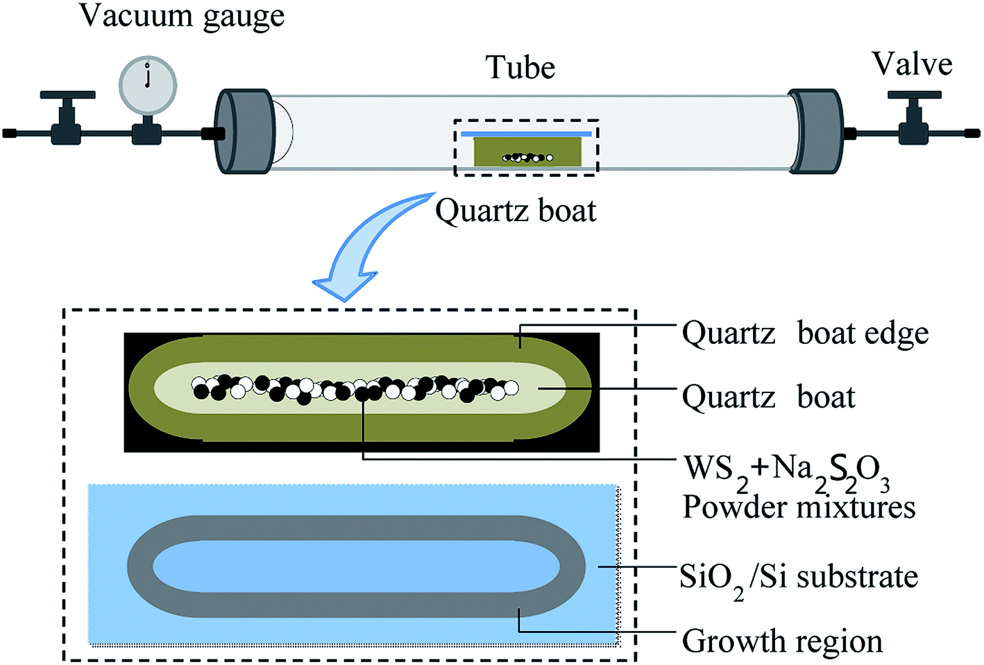 | ||
| Fig. 1 Schematic diagram of monolayer WS2 growth setup (upper), quartz boat and precursor (middle) and growth region (bottom) on SiO2/Si substrate. Growth zone shape is consistent with the edge of the quartz boat. | ||
Characterization
Optical and photoluminescence (PL) imaging was taken on a Jiangnan MV3000 digital microscope and a Nib400 fluorescence microscope (Jiangnan Novel Optics Co., Ltd.), respectively. Scanning electron microscopy (SEM) was conducted on a desktop scanning electron microscope (COXEM EM-30 AX Plus). PL and Raman spectra were acquired on a home-built Raman system, consisting of an inverted microscope (Ti eclipse, Nikon), a Raman spectrometer (iHR320, Horiba) with a CCD camera (Syncerity, Horiba) and a semiconductor laser at 532 nm.3. Results and discussion
We observed the triangular WS2 crystals were grown on the substrate. Fig. 2a and c show optical microscopy image of WS2 layers with a triangular shape. Different contrast colors represent different thickness of WS2 (see discussion in Fig. 3). The triangular areas circled in black, red, green and blue colors are bulk, monolayer, bilayer and multilayer in Fig. 2c, respectively. The size of the monolayer WS2 domain is ca. 12.7 μm. The possible reason to why the domain cannot grow up is the low surface energy of the substrate. The hexagonal WS2 crystal can be assumed to begin from a hexagonal nucleus with three sides of W atom terminations and three sides of S atom terminations. When the W![[thin space (1/6-em)]](https://www.rsc.org/images/entities/char_2009.gif) :S atomic ratio is less than 1:2, W terminations will grow faster than S terminations to become smaller or disappear until the hexagonal WS2 crystal grows to triangular in S rich structure. When the W:S atomic ratio is larger than 1:2, S terminations will grow faster than W terminations to become smaller or disappear until the hexagonal WS2 crystal grows to triangular in W rich structure. Both of these two cases could result in triangular shape WS2 growth. Therefore, the unbalanced the S and W termination growth at three sides of original hexagon could result in triangular WS2 growth.53,54 In this experiment, S source is sufficient from Na2S2O3, resulting in triangular WS2 growth.
:S atomic ratio is less than 1:2, W terminations will grow faster than S terminations to become smaller or disappear until the hexagonal WS2 crystal grows to triangular in S rich structure. When the W:S atomic ratio is larger than 1:2, S terminations will grow faster than W terminations to become smaller or disappear until the hexagonal WS2 crystal grows to triangular in W rich structure. Both of these two cases could result in triangular shape WS2 growth. Therefore, the unbalanced the S and W termination growth at three sides of original hexagon could result in triangular WS2 growth.53,54 In this experiment, S source is sufficient from Na2S2O3, resulting in triangular WS2 growth.
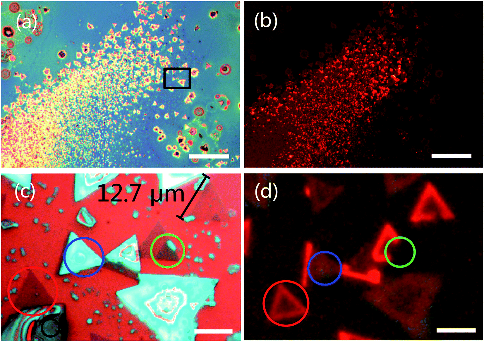 | ||
| Fig. 2 Optical microscopy (a) and photoluminescence (PL) (b) images of WS2 layers grown on SiO2/Si substrate. (c) Magnified optical microscopy and corresponding PL images taken from the boxed area in (a). (a) and (b) were taken at same location. The scale bars in figure (a) and (b) represent 100 μm, and 10 μm in (c) and (d). The red color in (b) and (d) is due to the PL emission of monolayer WS2. | ||
Fig. 2b and d show PL images from monolayer WS2 with 485 nm excitation wavelengths. Being different from the indirect band gap of multilayer, monolayer has a direct band structure with high external quantum efficiency. Therefore, we only observed bright PL emission from monolayer WS2 with 485 nm excitation wavelengths in Fig. 2b and d. Clearly, the edge of the WS2 domain (circled in red color in Fig. 2d) shows intensive PL emission. Inhomogeneous PL intensity within a monolayer domain (circled in red color in Fig. 2d) is due to the uniformity of composition and defects from the center to the edge.52
Raman spectrum is commonly used to identify the layer number of WS2 layer. Fig. 3a shows Raman spectra of WS2 layers at room temperature with 532 nm laser excitation corresponding to the marked regions in Fig. 2c. The Raman data was calibrated by the Raman peak of Si at 520 cm−1. Two main peaks at 351.1 cm−1 and 417.3 cm−1 are characteristic Raman peaks of monolayer WS2. The peak at 351.1 cm−1 is due to the in-plane phonon mode E12g, and 417.3 cm−1 for the out-of plane mode A1g. Therefore, the triangular domain circled in red color in Fig. 2c is monolayer WS2. The peak position and peak frequency difference between the two modes are the function of the number of WS2 layers. With the increase of the layer number, the E12g peak position decreases from 351.1 cm−1 of monolayer to 348.3 cm−1 of bulk; and the A1g peak position increases from 417.3 cm−1 of monolayer to 419.4 cm−1 of bulk. The peak frequency difference increases with the increase of the thickness shown in Fig. 3b. The frequency differences are 66.2 cm−1, 69.2 cm−1, 70.9 cm−1, and 71.1 cm−1 corresponding to monolayer, bilayer, multilayer and bulk, respectively.
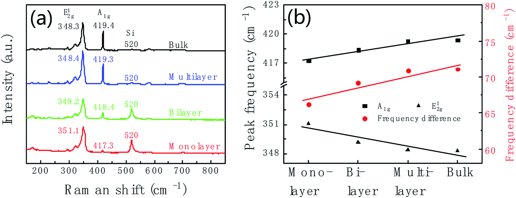 | ||
| Fig. 3 (a) Raman spectra of monolayer (red line), bilayer (green line), multilayer (blue line) and bulk (black line) WS2 corresponding to the sample in Fig. 2c. (b) Thickness dependent of Raman peak position and the peak frequency difference between E12g and A1g. | ||
Fig. 4 shows the thickness-dependent PL spectra of WS2. An intense PL emission peak in the monolayer (red line) at 636.2 nm is observed, which is due to the A− exciton emission. Compare to the monolayer, the PL intensity of bilayer (green line) is decreased by ca. 10-fold. For the multilayer (blue line), the PL intensity was further decreased. In bulk WS2 (black line), PL emission is hardly observed. Different behaviors in PL lie in the different band gap structures. Not like multilayer, monolayer has a direct band gap structure thus resulting in the intense PL emission. In addition, the PL peak position shows blueshift. We suspect the blueshift maybe be due to the defects and stress in the sample.55,56
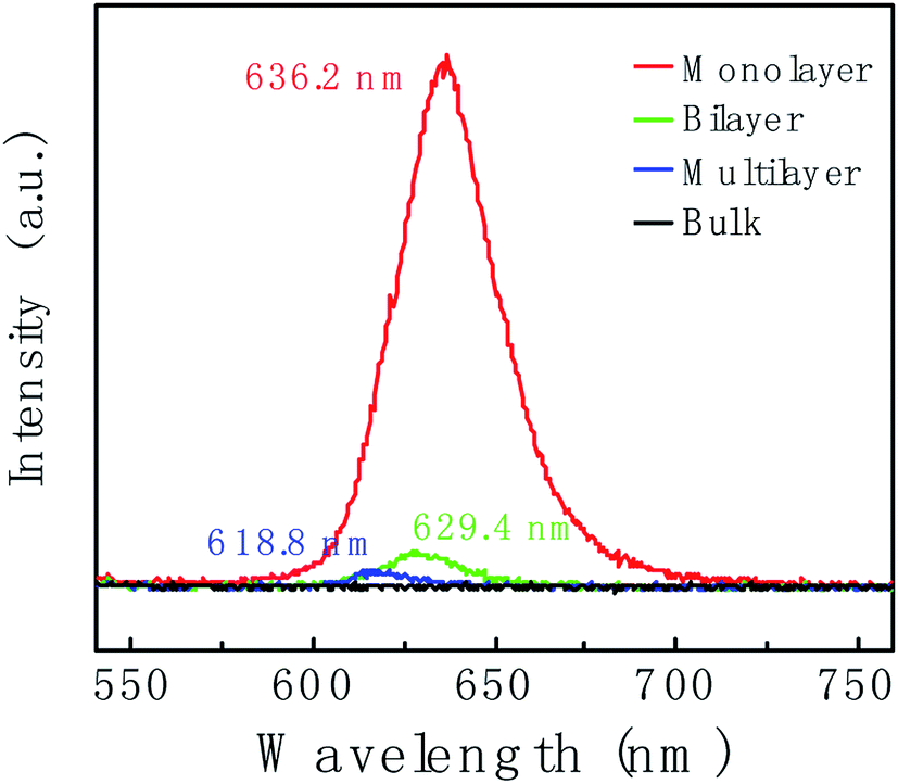 | ||
| Fig. 4 Photoluminescence (PL) spectra of WS2 layers corresponding to the region marked with a red circle, blue circle, green circle and black circle in Fig. 2c, respectively. | ||
Besides the triangular WS2 domains, we also observed the leaf-like WS2 film in Fig. 5. Fig. 5a and c are the optical microscopy images of the leaf-like WS2 film. Fig. 5d is the PL image corresponding to the sample in Fig. 5c. The bright red color is due to the monolayer. The shape size is up to 1150 μm (Fig. 5a). Inside is bulk WS2 (marked with black dot in Fig. 5b). Around the bulk WS2 is multilayer WS2 (dark lines in Fig. 5d) extending in all direction like leaf veins. Continuous monolayer WS2 (red color in Fig. 5d) connects the multilayer. The thickness is determined by following Raman and PL data in Fig. 6. This unique interconnection of the WS2 domains will benefit the future large-scale application in optoelectronics such as photodetectors in which the monolayer of WS2 could capture the excitation light signal and the generated free carriers could transport through the “leaf veins” channels of the multilayer of WS2.
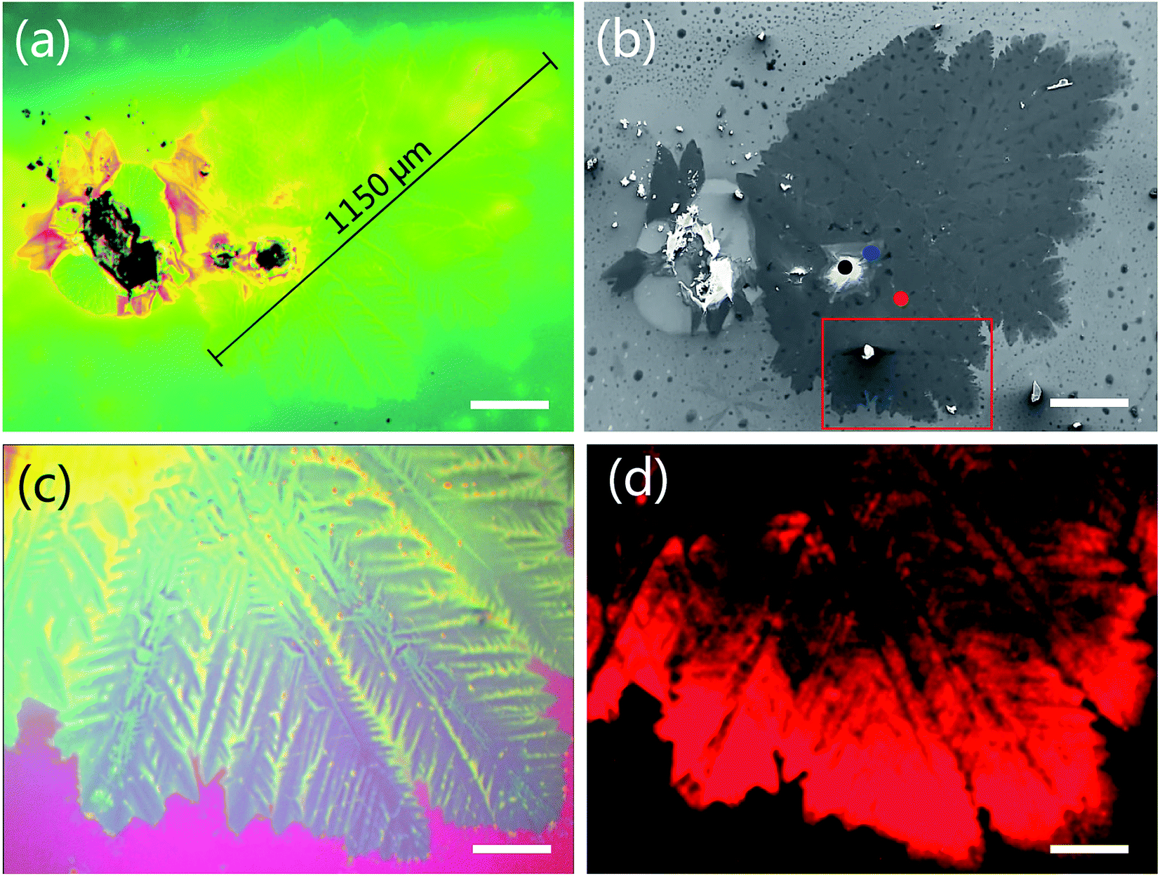 | ||
| Fig. 5 Optical microscopy (a) and SEM (b) images of WS2 film taken at the same location. (c) Magnified optical microscopy image of (a). (d) The photoluminescence (PL) image corresponding to the sample of (c). (c) and (d) are taken at the same location. The red color in (d) is due to the PL emission of monolayer WS2. The scale bars in figure (a), (b), (c) and (d) represent 200 μm, 200 μm, 50 μm and 50 μm, respectively. | ||
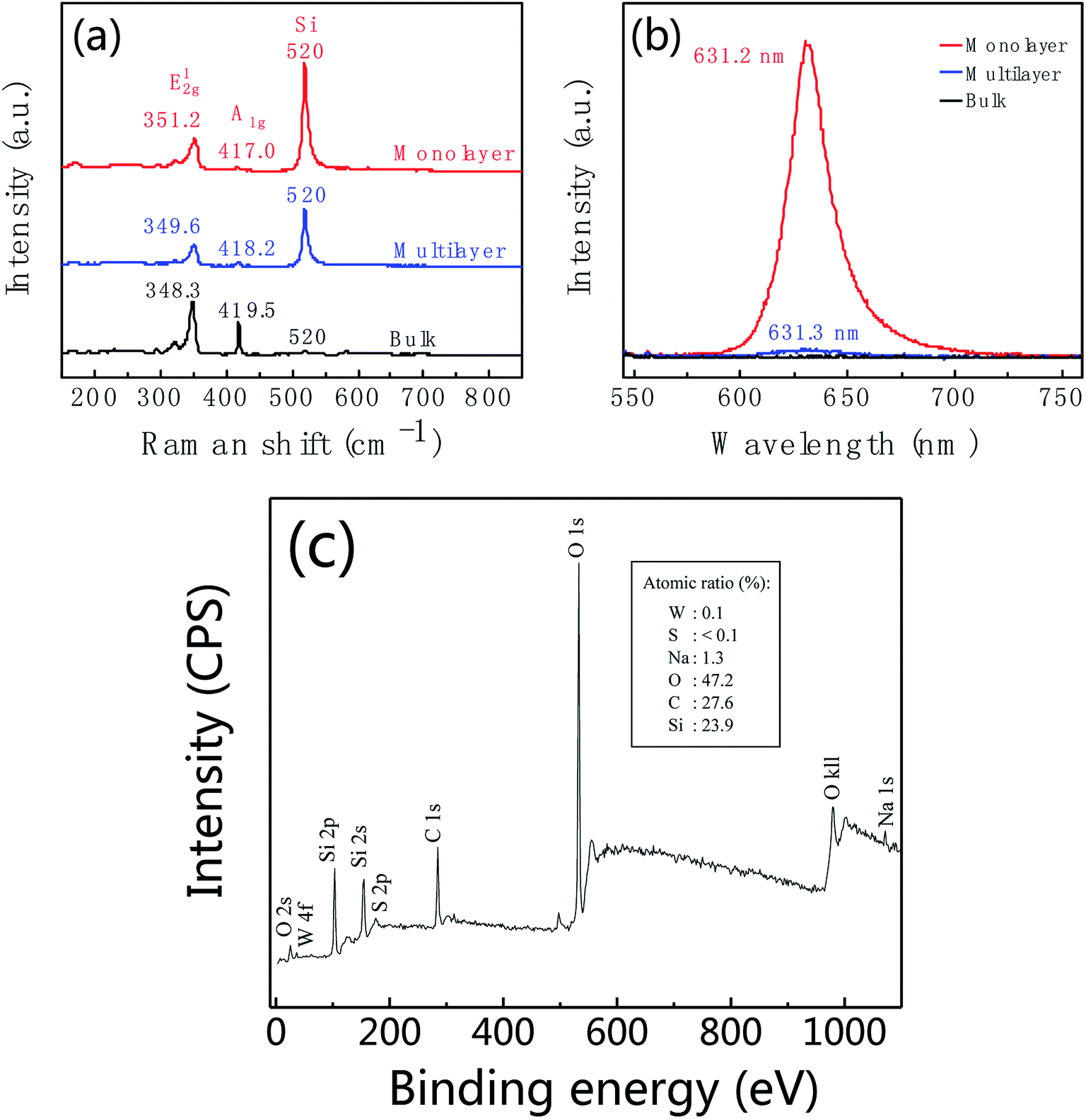
Fig. 6a and b shows the Raman and PL spectra of WS2 at different locations corresponding to the regions marked with red, blue and black spots in Fig. 5b. For the region marked with red color, Raman peaks of E12g and A1g are at 351.2 cm−1 and 417.0 cm−1, respectively, with peak frequency difference of 65.8 cm−1 (red curve in Fig. 6a). As well as this region shows intensive PL emission at 631.2 nm. These features indicate that the region marked with a red dot in Fig. 5b is monolayer WS2. By further analysis, we found the regions marked with blue and black dots in Fig. 5b are multilayer and bulk, respectively. Fig. 6c is XPS of leaf-like domain showing W atomic ratio is 0.1% and S atomic ratio is <0.1%. Therefore, W:S atomic ratio is larger than 1:2. Carbon is from CO2 which was adsorbed on the surface of sample. Silicon is from substrate.
 | ||
| Fig. 6 Raman (a) and photoluminescence (b) spectra of WS2 taken from the regions marked with red, blue and black spots in Fig. 5b. (c) XPS of leaf-like domain of as-prepared WS2. Insert is atomic ratio. | ||
Here, the leaf-like shape WS2 growth mechanism should be different from the triangular WS2 and more like kinetically limited growth (Fig. 7). We suspect that the leaf-like shape is due to the preferential orientation growth. The above-mentioned triangle growth is due to preferential growth with W terminations. However, the preferential growth of leaf-like shape is S terminations. Sodium ions (Na+) from the sodium triosulfate (Na2S2O3) precursor is diffused all over the Si substrate during the heating up steps, wherein S terminations will absorb the Na+ to form sodium-passivated S terminations, resulting the terminated chemical reaction between S and W and the further growth of WS2 (Fig. 7a). At 500 °C, Na+ is physically adsorbed on substrate surface, so the absorption quantity is so little that there is no obvious effect on resulting sodium-passivated S termination. Thus, preferential growth of triangle shape is W terminations. At 700 °C, Na+ is chemically adsorbed on substrate surface, so the absorption quantity is enough to result sodium-passivated S termination. As a result, the preferential growth of leaf-like shape is S terminations (Fig. 7b) which is consistent with the XPS results that the W and S atomic ratio is larger than 1:2. The defects are introduced combined with the faster growth and lead to the multilayer growth with Stranski–Krastanow mode (SK mode) which refers to layer plus island growth: 2D film grows on the surface of substrate and there is distortion due to lattice mismatch between film and substrate. Then, the 2D film will adsorb the deposited atoms, forming islands in the way of nucleation growth, and eventually grows into film. Therefore, the “leaf veins” (in Fig. 5c and d) are produced. Followed the growth of “leaf veins”, is the relatively slow-growing S terminations as shown in the inset of Fig. 7b, where triangular shape of WS2 could be formed to successfully fill the gaps among the branched leaf veins. Therefore, the interconnected WS2 in large scale has been formed.
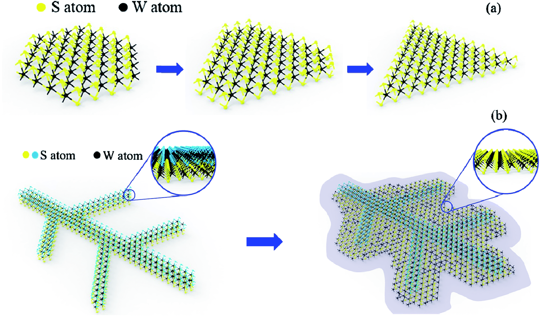 | ||
| Fig. 7 Schematic drawing of the growth mechanism of (a) triangular WS2 and (b) leaf-like WS2. | ||
4. Conclusion
In conclusion, we have successfully prepared WS2 layers by CVD with the WS2 and Na2S2O3 as precursors. Na2S2O3 used as sulfur precursor and molten salt has a significant effect on the film growth. Triangular and leaf-like shapes of WS2 film were obtained. The S-termination could absorb the Na+ to form sodium-passivated S terminations and terminate the further growth of WS2, resulting the triangular shape of WS2. On contrast, the W-termination grows much faster than the S-termination, resulting the leaf vein shape growth of WS2. Followed the growth of “leaf veins”, there are more locations of S-termination in the branched veins of WS2 which is favorable for triangular WS2 growth to fill the gaps among the various veins in the leaf structured WS2. Therefore, the controllable WS2 layers have been demonstrated with Na2S2O3 precursors as growth motivators which could provide informative guidance for future large-scale 2D growth.Conflicts of interest
There are no conflicts of interest to declare.Acknowledgements
This work was supported by the Natural Science Foundation of Zhejiang Province, China Projects (LY16E020008) and Chinese NSF Projects (61106100). We thank Shenzhen Municipal Development and Reform Commission, and New Energy Technology Engineering Laboratory (Grant Number: SDRC [2016]172).References
- Q. H. Wang, K. Kalantar-Zadeh, A. Kis, J. N. Coleman and M. S. Strano, Nat. Nanotechnol., 2012, 7, 699–712 CrossRef CAS PubMed.
- Z. H. Xu, Y. F. Lv, F. Huang, C. Zhao, S. C. Zhao and G. D. Wei, Materials, 2019, 12, 1883 CrossRef PubMed.
- Y. Chen, L. Gan, H. Q. Li, Y. Ma and T. Y. Zhai, Adv. Mater., 2017, 29, 1603550 CrossRef PubMed.
- W. H. Yang, J. Z. Shang, J. P. Wang, X. N. Shen, B. C. Cao, N. Peimyoo, C. J. Zou, Y. Chen, Y. L. Wang, C. X. Cong, W. Huang and T. Yu, Nano Lett., 2016, 16, 1560–1567 CrossRef CAS PubMed.
- M. Feierabend, Z. Khatibi, G. Berghauser and E. Malic, Phys. Rev. B, 2019, 99, 195454 CrossRef CAS.
- D. Voiry, H. Yamaguchi, J. W. Li, R. Silva, D. C. B. Alves, T. Fujita, M. W. Chen, T. Asefa, V. B. Shenoy, G. Eda and M. Chhowalla, Nat. Mater., 2013, 12, 850–855 CrossRef CAS PubMed.
- S. M. Notley, J. Colloid Interface Sci., 2013, 396, 160–164 CrossRef CAS PubMed.
- B. K. M. a. S. R. Morrison, J. Appl. Phys., 1988, 63, 4970–4974 CrossRef.
- L. H. Yuwen, H. Yu, X. R. Yang, J. J. Zhou, Q. Zhang, Y. Q. Zhang, Z. M. Luo, S. Su and L. H. Wang, Chem. Commun., 2016, 52, 529–532 RSC.
- A. Ghorai, A. Midya, R. Maiti and S. K. Ray, Dalton Trans., 2016, 45, 14979–14987 RSC.
- W. J. Zhao, Z. Ghorannevis, L. Q. Chu, M. L. Toh, C. Kloc, P. H. Tan and G. Eda, ACS Nano, 2013, 7, 791–797 CrossRef CAS PubMed.
- Z. Liu, K. Suenaga, Z. Y. Wang, Z. J. Shi, E. Okunishi and S. Iijima, Nat. Commun., 2011, 2, 213 CrossRef PubMed.
- A. S. George, Z. Mutlu, R. Ionescu, R. J. Wu, J. S. Jeong, H. H. Bay, Y. Chai, K. A. Mkhoyan, M. Ozkan and C. S. Ozkan, Adv. Funct. Mater., 2014, 24, 7461–7466 CrossRef CAS.
- K. C. Kwon, C. Kim, Q. V. Le, S. Gim, J. M. Jeon, J. Y. Ham, J. L. Lee, H. W. Jang and S. Y. Kim, ACS Nano, 2015, 9, 4146–4155 CrossRef CAS PubMed.
- D. Barrera, Q. X. Wang, Y. J. Lee, L. X. Cheng, M. J. Kim, J. Kim and J. W. P. Hsu, J. Mater. Chem. C, 2017, 5, 2859–2864 RSC.
- Y. Zhang, Y. F. Zhang, Q. Q. Ji, J. Ju, H. T. Yuan, J. P. Shi, T. Gao, D. L. Ma, M. X. Liu, Y. B. Chen, X. J. Song, H. Y. Hwang, Y. Cui and Z. F. Liu, ACS Nano, 2013, 7, 8963–8971 CrossRef CAS PubMed.
- R. Gatensby, N. McEvoy, K. Lee, T. Hallam, N. C. Berner, E. Rezvani, S. Winters, M. O'Brien and G. S. Duesberg, Appl. Surf. Sci., 2014, 297, 139–146 CrossRef CAS.
- J. G. Song, J. Park, W. Lee, T. Choi, H. Jung, C. W. Lee, S. H. Hwang, J. M. Myoung, J. H. Jung, S. H. Kim, C. Lansalot-Matras and H. Kim, ACS Nano, 2013, 7, 11333–11340 CrossRef CAS PubMed.
- B. Groven, M. Heyne, A. N. Mehta, H. Bender, T. Nuytten, J. Meersschaut, T. Conard, P. Verdonck, S. Van Elshocht, W. Vandervorst, S. De Gendt, M. Heyns, I. Radu, M. Caymax and A. Delabie, Chem. Mater., 2017, 29, 2927–2938 CrossRef CAS.
- M. E. McConney, N. R. Glavin, A. T. Juhl, M. H. Check, M. F. Durstock, A. A. Voevodin, T. E. Shelton, J. E. Bultman, J. Hu, M. L. Jespersen, M. K. Gupta, R. D. Naguy, J. G. Colborn, A. Haque, P. T. Hagerty, R. E. Stevenson and C. Muratore, J. Mater. Res., 2016, 31, 975 CrossRef.
- W. F. Yang, H. Kawai, M. Bosman, B. S. Tang, J. W. Chai, W. L. Tay, J. Yang, H. L. Seng, H. L. Zhu, H. Gong, H. F. Liu, K. E. J. Goh, S. J. Wang and D. Z. Chi, Nanoscale, 2018, 10, 22927–22936 RSC.
- J. Park, W. Lee, T. Choi, S. H. Hwang, J. M. Myoung, J. H. Jung, S. H. Kim and H. Kim, Nanoscale, 2015, 7, 1308–1313 RSC.
- G. V. Bianco, M. Losurdo, M. M. Giangregorio, A. Sacchetti, P. Prete, N. Lovergine, P. Capezzuto and G. Bruno, RSC Adv., 2015, 5, 98700–98708 RSC.
- S. J. Yun, S. H. Chae, H. Kim, J. C. Park, J. H. Park, G. H. Han, J. S. Lee, S. M. Kim, H. M. Oh, J. Seok, M. S. Jeong, K. K. Kim and Y. H. Lee, ACS Nano, 2015, 9, 5510–5519 CrossRef CAS PubMed.
- Y. P. Fan, G. L. Hao, S. W. Luo, X. Qi, H. X. Li, L. Ren and J. X. Zhong, AIP Adv., 2014, 4, 057105 CrossRef.
- X. D. Duan, C. Wang, J. C. Shaw, R. Cheng, Y. Chen, H. L. Li, X. P. Wu, Y. Tang, Q. L. Zhang, A. L. Pan, J. H. Jiang, R. Q. Yu, Y. Huang and X. F. Duan, Nat. Nanotechnol., 2014, 9, 1024–1030 CrossRef CAS PubMed.
- Q. Fu, W. H. Wang, L. Yang, J. Huang, J. Y. Zhang and B. Xiang, RSC Adv., 2015, 5, 15795–15799 RSC.
- C. Y. Lan, C. Li, Y. Yin and Y. Liu, Nanoscale, 2015, 7, 17980 RSC.
- J. G. Song, G. H. Ryu, S. J. Lee, S. Sim, C. W. Lee, T. Choi, H. Jung, Y. Kim, Z. Lee, J. M. Myoung, C. Dussarrat, C. Lansalot-Matras, J. Park, H. Choi and H. Kim, Nat. Commun., 2015, 6, 7817 CrossRef PubMed.
- Y. Gao, Z. B. Liu, D. M. Sun, L. Huang, L. P. Ma, L. C. Yin, T. Ma, Z. Y. Zhang, X. L. Ma, L. M. Peng, H. M. Cheng and W. C. Ren, Nat. Commun., 2015, 6, 8569 CrossRef CAS PubMed.
- P. V. Sarma, P. D. Patil, P. K. Barman, R. N. Kini and M. M. Shaijumon, RSC Adv., 2016, 6, 376–382 RSC.
- S. Hussain, M. F. Khan, M. A. Shehzad, D. Vikraman, M. Z. Iqbal, D. C. Choi, W. Song, K. S. An, Y. Seo, J. Eom, W. G. Lee and J. Jung, J. Mater. Chem. C, 2016, 4, 7846–7852 RSC.
- S. Hu, X. F. Wang, L. Meng and X. H. Yan, J. Mater. Sci., 2017, 52, 7215–7223 CrossRef CAS.
- P. Y. Liu, T. Luo, J. Xing, H. Xu, H. Y. Hao, H. Liu and J. J. Dong, Nanoscale Res. Lett., 2017, 12, 558 CrossRef PubMed.
- F. F. Lan, R. X. Yang, Y. K. Xu, S. Y. Qian, S. Zhang, H. J. Cheng and Y. Zhang, Nanomaterials, 2018, 8, 100 CrossRef PubMed.
- P. Kumar and V. Balakrishnan, Appl. Surf. Sci., 2018, 436, 846–853 CrossRef CAS.
- W. Zeng, L. P. Feng, J. Su, H. X. Pan and Z. T. Liu, J. Alloys Compd., 2018, 745, 834–839 CrossRef CAS.
- C. Y. Lan, Z. Y. Zhou, Z. F. Zhou, C. Li, L. Shu, L. F. Shen, D. P. Li, R. T. Dong, S. P. Yip and J. Ho, Nano Res., 2018, 11, 3371–3384 CrossRef CAS.
- Y. Yu, Z. Y. Wang, J. L. Wei, W. Y. Zhao, X. Lin, Z. M. Jin, W. M. Liu and G. H. Ma, J. Phys.: Condens. Matter, 2018, 30, 495701 CrossRef PubMed.
- B. Shi, D. M. Zhou, S. X. Fang, K. Djebbi, S. L. Feng, H. Q. Zhao, C. Tlili and D. Q. Wang, Nanomaterials, 2019, 9, 578 CrossRef CAS PubMed.
- S. H. Zhang, J. Y. Wang, Y. Lu, W. W. Hou, K. Cao, S. H. Guo, Z. D. Wang and L. Wang, Chem. Phys., 2019, 523, 106–109 CrossRef CAS.
- B. Zhou, C. Z. Su, B. Shi, Y. J. Wang, L. Yu, S. Feng and D. Wang, Int. Conf. Manipulation, Manuf. Meas. Int. Conf. Manipulation, Manuf. Meas. Nanoscale, 2017, 379–383 Search PubMed.
- M. E. Pam, Y. Shi, L. K. Ang and H. Y. Yang, IEEE Nanotechnology Magazine, 2017, 91–92 Search PubMed.
- C. R. Wu, X. R. Chang, C. H. Wu and S. Y. Lin, Sci. Rep., 2017, 7, 42146 CrossRef CAS PubMed.
- J. D. Cain, F. Y. Shi, J. S. Wu and V. P. Dravid, ACS Nano, 2016, 10, 5440–5445 CrossRef CAS PubMed.
- S. S. Li, S. F. Wang, D. M. Tang, W. J. Zhao, H. L. Xu, L. Q. Chu, Y. Bando, D. Golberg and G. Eda, Appl. Mater. Today, 2015, 1, 60–66 CrossRef.
- J. D. Zhou, J. H. Lin, X. W. Huang, Y. Zhou, Y. Chen, J. Xia, H. Wang, Y. Xie, H. M. Yu, J. C. Lei, D. Wu, F. C. Liu, Q. D. Fu, Q. S. Zeng, C. H. Hsu, C. L. Yang, L. Lu, T. Yu, Z. X. Shen, H. Lin, B. I. Yakobson, Q. Liu, K. Suenaga, G. T. Liu and Z. Liu, Nature, 2018, 556, 355–359 CrossRef CAS PubMed.
- B. J. Modtland, E. Navarro-Moratalla, X. Ji, M. Baldo and J. Kong, Small, 2017, 13, 1701232 CrossRef PubMed.
- Z. Wang, Y. Xie, H. L. Wang, R. X. Wu, T. Nan, Y. J. Zhan, J. Sun, T. Jiang, Y. Zhao, Y. M. Lei, M. Yang, W. D. Wang, Q. Zhu, X. H. Ma and Y. Hao, Nanotechnology, 2017, 28, 325602 CrossRef PubMed.
- Y. C. Lin, C. H. Yeh, H. C. Lin, M. D. Siao, Z. Liu, H. Nakajima, T. Okazaki, M. Y. Chou, K. Suenaga and P. W. Chiu, ACS Nano, 2018, 12, 12080–12088 CrossRef CAS PubMed.
- S. Sasaki, Y. Kobayashi, Z. Liu, K. Suenaga, Y. Maniwa, Y. Miyauchi and Y. Miyata, Appl. Phys. Express, 2016, 9, 071201 CrossRef.
- Y. Zhu, H. Yi, Q. Y. Hao, J. D. Liu, Y. X. Ke, Z. Wang, D. Y. Fan and W. J. Zhang, Appl. Surf. Sci., 2019, 485, 101–107 CrossRef CAS.
- S. S. Wang, Y. M. Rong, Y. Fan, M. Pacios, H. Bhaskaran, K. He and J. H. Warner, Chem. Mater., 2014, 26, 6371–6379 CrossRef CAS.
- L. Dong, Y. Wang, J. Sun, C. Pan, Q. Zhang, L. Gu, B. Wan, C. Song, F. Pan, C. Wang, Z. Tang and J. Zhang, 2D Mater, 2019, 6, 015007 CrossRef.
- F. Wang, I. A. Kinloch, D. Wolverson, R. Tenne, A. Zak, E. O'Connell, U. Bangert and R. J. Young, 2D Mater, 2017, 4, 015007 CrossRef.
- G. Zhang and Y. W. Zhang, Mech. Mater., 2015, 91, 382–398 CrossRef.
| This journal is © The Royal Society of Chemistry 2019 |