
 Open Access Article
 This Open Access Article is licensed under a Creative Commons Attribution-Non Commercial 3.0 Unported Licence
Two-dimensional polar metals in KNbO3/BaTiO3 superlattices: first-principle calculations†
Gang Li‡
a,
Huiyu Huang‡a,
Shaoqin Penga,
Ying Xiongb,
Yongguang Xiaoa,
Shaoan Yan c,
Yanwei Caod,
Minghua Tang*a and
Zheng Li*a
c,
Yanwei Caod,
Minghua Tang*a and
Zheng Li*a
aSchool of Materials Science and Engineering, Xiangtan University, Xiangtan, Hunan 411105, China. E-mail: tangminghua@xtu.edu.cn; lizheng@xtu.edu.cn
bSchool of Mathematics and Computational Science, Xiangtan University, Xiangtan 411105, China
cSchool of Mechanical Engineering, Xiangtan University, Xiangtan 411105, China
dCAS Key Laboratory of Magnetic Materials and Devices, Ningbo Institute of Materials Technology and Engineering, Chinese Academy of Sciences, Ningbo, Zhejiang 315201, China
First published on 1st November 2019
Abstract
Polar metals, commonly defined by the coexistence of polar structure and metallicity, are thought to be scarce because free carriers eliminate internal dipoles that may arise owing to asymmetric charge distributions. By using first-principle electronic structure calculations, we explored the possibility of producing metallic states in the polar/nonpolar KNbO3/BaTiO3 superlattice (SL) composed of two prototypical ferroelectric materials: BaTiO3 (BTO) and KNbO3 (KNO). Two types of polar/nonpolar interfaces, p-type (KO)−/(TiO2)0 and n-type (NbO2)+/(BaO)0, which can be constituted into two symmetric NbO2/BaO–NbO2/BaO (NN-type) and KO/TiO2–KO/TiO2 (PP-type) SL, as well as one asymmetric KO/TiO2–NbO2/BaO (PN-type) SL. The spatial distribution of ferroelectric distortions and their conductive properties are found to be extraordinarily sensitive to the interfacial configurations. An insulator-to-metal transition is found in each unit cell of the symmetric interfacial SL models: one exhibiting quasi-two-dimensional n-type conductivity for NN-type SL, while the other being quasi-two-dimensional p-type conductivity for PP-type SL. The anisotropic coexistence of in-plane orientation of free carriers and out-of-plane orientation of ferroelectric polarization in KNO/BTO SL indicates that in-plane free carriers can not eliminate the out-of-plane dipoles. Our results provide a road map to create two-dimensional polar metals in insulating perovskite oxide SL, which is expected to promote applications of new quantum devices.
1 Introduction
Metals cannot exhibit ferroelectricity because free carriers eliminate static internal electric fields that may arise owing to asymmetric charge distributions.1 But in 1965 Anderson and Blount2 first predicted that two seemingly incompatible properties, i.e., ferroelectricity and metallicity, could coexist in polar metals (also called ferroelectric metals). Such unique and counter-intuitive cases have puzzled us for half a century until LiOsO3 was discovered,3 whose metal behavior was found unchanged but rather it underwent a structural phase transition around in 140 K. In addition to the intrinsic polar metals,4–8 structural phase transitions can occur in metallic noncentrosymmetric oxides, designed by “weak-coupling” mechanism (e.g., SrCaRu2O6)9 or “geometric design” method (e.g., NdNiO3).10 However, a wide variety of materials surveys have indicated that metal-based oxide compounds are extremely rare being polar metals.8,11,12Because of the lack of metal-based polar metals, it is urgent to design easily-realizable polar metals for further research and practical applications. Analogous to metal-based polar metals with structural phase transitions,3–12 ferroelectric-based polar metals are another category of polar metals with insulator–metal transitions.13–20 Compared with the structural phase transitions hardly occurred in metals, insulator–metal transitions are prone to be realized in ferroelectrics, and they have broad practical application prospects due to the enormous range of ferroelectrics and their compounds readily available at room temperature. A conventional approach to achieve metal behavior in ferroelectrics is to introduce electron carriers into the ferroelectrics by injecting vacancies or doping,13–19 e.g., O vacancies in BTO,13,14 element or electrostatic doping in BTO.15–19 The polarization displacements show a rapid decrease with increasing carrier concentration. But recently, Cao et al.20 created a room temperature quasi-two-dimensional polar metal with a tri-layer BaTiO3/SrTiO3/LaTiO3 SL, the two-dimensional electron gas (2DEG) at the interface of SrTiO3/LaTiO3 provides metal conductivity and simultaneously realizes ferroelectric structure phase transition by BaTiO3. This approach provides a new road map to create and enrich polar metals in perovskite oxide compositions and the discovery of new physical phenomena.
The formation of 2DEG or two-dimensional hole gas (2DHG) is one of the most important ways to realize the interfacial conductivity of insulating perovskite oxide heterostructures (HS) or SL.21–30 Since the discovery of 2DEG at the n-type interface in LaAlO3/SrTiO3 HS,21 based on experimental and theoretical studies, a lot of intriguing physical properties have been explored in n-type interface of perovskite oxide HS.21–26 Although theoretical investigations have predicted a 2DHG exists in p-type interfaces,27 most of the experimentally verified p-type interfaces exhibit an insulating behavior.21,28 Excitingly, 2DHG was first observed on oxide p-type interfaces of SrTiO3/LaAlO3/SrTiO3 HS very recently,29 and it was found that eliminating ionic point defects is the key to realize a 2DHG. According to the formation mechanisms of interfacial conductivity in perovskite oxide compounds, there are essentially two main categories of mechanisms that can form the 2DEG or 2DHG.30,31 The first one is polar discontinuity,21–26,31–35 i.e., polar catastrophe, including polar/nonpolar and polar/polar interfacial structures. This interfacial metal behavior formation mechanism is principally attributed to the intrinsic electronic reconstruction. For example, for a polar/nonpolar interfacial structure, a 2DEG exists at the n-type (LaO)+/(TiO2)0 interface21 and a 2DHG exists at the p-type (AlO2)−/(SrO)0 interface29 in the LaAlO3/SrTiO3 system. While for the polar/polar interfacial structure, such as n-type (LaO)1+/(TaO2)1+ in the LaAlO3/KTaO3 system,31,36 two donor layers make it to have larger interface carrier density than that in the polar/nonpolar LaAlO3/SrTiO3 system. The second formation mechanism is to form interfacial metal states at the nonpolar/nonpolar interface via the polarization discontinuity. The interfacial metal states here are more sensitive to the polarization orientation rather than the interfacial configuration.30,36–41 For example for the CaHfO3/SrTiO3 system,37,38 when the polarization direction is toward the interface, electrons are transferred from CaHfO3 to SrTiO3 driven by the polarization field, resulting in the formation of a 2DEG at the SrTiO3 interface. Whereas when the polarization reverses backward at the interface, electrons are transferred from SrTiO3 into CaHfO3, forming a 2DHG at SrTiO3 interface.
In this work, to reveal the underlying relationship of electrical conductivity and the intensity and stability of polarization in ferroelectric-based polar metals, we designed a KNO/BTO SL composed of two prototypical ferroelectric materials, and surveyed two symmetric and one asymmetric category of KNO/BTO SL models. We also investigated the magnitude and robustness of polarization, electronic properties, and band diagram in the KNO/BTO SL by using the density functional theory (DFT) calculations. The design idea is to obtain the interfacial metal behavior at the polar/nonpolar interface via polar discontinuity and polarization discontinuity, where the electrostatic field generated by polarization plays a major role in the redistribution of electrons from the interface to other regions. We have found that the spatial distribution of polarization distortions, the robustness of polarization, and conductivity are quite sensitive to the interface structure. Moreover, there exist insulator–metal transitions in two symmetric SL models, and these SL models exhibit quasi-two-dimensional conductivity. In addition, the relationship between the direction and intensity of polarization versus the concentration of free carriers in each cell are elucidated in this paper.
2 Structural modeling and computational details
At room temperature, bulk KNO42 and BTO43 compounds crystallize in a tetragonal phase (space group no. 99, P4mm), and all of them are prototypical ferroelectric materials. The experimental spontaneous polarizations are 37 μC cm−2 and 27 μC cm−2,44,45 apart. The DFT equilibrium (experimental) lattice constant a is 4.022 Å (4.003 Å)42 and 4.012 Å (3.996 Å)43 for KNO and BTO, respectively. The lattice mismatch f between the KNO and BTO is defined as f = (a1 − a2)/a2, where a1 and a2 are the free lattice constants of KNO and BTO, respectively. Therefore it can be considered that the KNO/BTO SL is unstrained because the lattice mismatch f between KNO and BTO is almost negligible.We employed a sandwich structural model to simulate the polar/nonpolar KNO/BTO SL, where two kinds of ferroelectric KNO and BTO were alternately stacked along the [001] orientation. The initial ferroelectric polarization direction along the +c-axis is defined as upward polarization (Pup). Correspondingly, downward polarization (Pdw) is represented along −c-axis. Here, two types of interface structures exist in our model, i.e., (KO)−/(TiO2)0 and (NbO2)+/(BaO)0. Hence, both types of interfacial configurations were modeled in our polar/nonpolar KNO/BTO SL system, which can structure three categories of KNO/BTO SL models. 4.5 or 4 monolayers of KNO and BTO are included in the symmetric and asymmetric model, separately. Illustrated in Fig. 1 are two symmetric NbO2/BaO–NbO2/BaO (NN-type) and KO/TiO2–KO/TiO2 (PP-type) interfacial SL models (Fig. 1(a and b)), and one asymmetric KO/TiO2–NbO2/BaO (PN-type) interfacial model considering the polarization orientation (Fig. 1(c and d)).
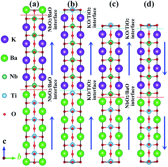 | ||
| Fig. 1 Side view of KNO/BTO SL for different interfacial structure, (a) NN-type, (b) PP-type, (c) PN-type with Pup, (d) PN-type with Pdw, the blue arrows represent the ferroelectric polarization direction, the red and cyan dot line represent the (NbO2)+/(BaO)0 and (KO)−/(TiO2)0 interface, respectively. | ||
Our DFT electronic structure calculations were implemented using the Vienna Ab initio Simulation Package (VASP).46,47 The projector augmented wave (PAW) potentials were used for treating electron–ion interactions,48 and the generalized gradient approximation (GGA) parametrized by Perdew–Burke–Ernzerhof (PBE) plus the on-site Coulomb interaction approach (GGA + U) were applied for the exchange-correlation functional.49 To appropriately describe the electronic states of strongly correlated Ti 3d and Nb 4d electrons, we calculated the Ev, Ec, Eg of BTO and KNO with different on-site Coulomb effective U values listed in Table S1 as ESI,† in which Ev of BTO was used as a reference. The on-site Coulomb effective U parameter value of 5.8 eV (ref. 50) and 5.0 eV (ref. 31) were used for Ti 3d orbitals and Nb 4d orbitals, respectively. A cutoff energy of 450 eV for the plane wave expansion was used. The Monkhorst–Pack k-point grids for Brillouin zone sampling were set to 9 × 9 × 2 for ionic relaxation and 25 × 25 × 3 for static calculations, respectively. All crystal structures relaxations were optimized until the Hellman–Feynman forces on the relaxed atoms were less than 0.01 eV Å−1. For the electronic self-consistency loop, total energy convergence was less than 10−6 eV per cell. The density of states (DOS) was calculated using a value of Gaussian smearing of 0.05 eV.
3 Results and discussion
3.1 Polarization displacement and polarization robustness
Polar metal is a material where polar crystal structure and metallicity coexist. For the purpose of probing whether the KNO/BTO SL is a polar metal, we first examined the ferroelectric polarization property of KNO/BTO SL. Even though we know that KNO and BTO are typical ferroelectric materials, it is necessary to verify whether ferroelectricity is possessed when they are composed of SLs with different interfacial structures. Therefore, ferroelectric displacements and the double-well potentials of KNO/BTO SLs with different interfacial structures were calculated, as shown in Fig. 2. In order to more intuitively inspect the change of cation–anion ferroelectric displacement and ferroelectric robustness in a SL, we give the relevant calculated values of bulk KNO and BTO as references. | ||
| Fig. 2 (a) Calculated layer-resolved Ti–O or Nb–O displacements in the KNO/BTO SL for different interfacial structure, the solid and hollow symbols indicate Pup and Pdw, respectively, the black arrows represent the polarization direction, the parallel orange (violet) dash line indicate Ti–O (Nb–O) displacement of bulk BTO (KNO), the vertical cyan short dot indicate interface of BTO/KNO SL. (b) Calculated total energy per unit cell as a function of polarization distortion for KNO/BTO SL with different interfacial structures as well as bulk KNO and BTO, in which λ = −1 (λ = 1) and λ = 0 represent the ferroelectric phase and the paraelectric phase, respectively. Note, the total energy per unit cell for the NN-type and PP-type SL is the total energy of the KNO/BTO SL divided by 9, while for the PN-type SL, it is divided by 8. | ||
For the Ti–O and Nb–O displacement of each atomic layer in KNO/BTO SLs with different interfacial structure as displayed in Fig. 2(a), we can see that the magnitude of polarization displacements are exceedingly sensitive to interfacial configuration in KNO/BTO SLs. Different polarization distortion patterns are formed in different interfacial configuration models because of different interfacial electronic reconstructions induced by polar catastrophe. In addition, the direction of polarization also has a certain influence on the spatial distribution of ferroelectric distortions, especially on the PN-type SL, displaying a completely different ferroelectric distortion pattern when polarization is flipped. But for two categories of the symmetric SL model, the NN-type and the PP-type SL, the spatial distribution of ferroelectric distortions in BTO and KNO region along the polarization direction are exactly the same for Pup state and Pdw state, thus the strength of total ferroelectric polarization remains unchanged even if the polarization is reversed. That is why, for the convenience of analyzing the symmetric interface SL model, only the Pup state needs to be considered.
In Fig. 2(a), for NN-type SL, along with the polarization direction, the magnitude of Ti–O displacement in the atomic layers in the BTO region shows a gradual decrease. While in the KNO region, the magnitude of Nb–O displacement in atomic layers manifests an abruptly decrease. By comparing with the reference value of bulk BTO or KNO, besides the NbO2 atomic layer of the left interface in the KNO region, we can clearly find that the magnitude of Ti–O and Nb–O displacements in other atomic layer is significantly smaller than the reference value, which indicates that NN-type SL reduces the strength of total polarization. The double-well potential in Fig. 2(b) can further verify this fact. The switch potential barrier height dE of the ferroelectrics is defined as the difference between the energy of the ferroelectric phase (λ = ±1) and the paraelectric phase (λ = 0). Large dE means that a ferroelectric has stronger stability, and implies a larger Curie temperature (TC, ferroelectric–paraelectric transition temperature). The dE value of the NN-type SL obviously is lower than that of either bulk BTO or KNO, which means that the polarization robustness is weakened in the NN-type SL. The itinerant electron generated at the n-type interface in the NN-type SL reduces the strength of polarization and stability, which is consistent with the previously reported finding that electron-doping in BTO reduces ferroelectric displacements.13
The evolution of ferroelectric displacements in the atomic layer along the polarization direction in the PP-type SL is completely opposite to that in the NN-type SL. The magnitude of Ti–O displacement in the BTO region shows a rapid increase and Nb–O displacement tardily increase in the KNO region. Surprisingly, toward the direction of polarization, the difference between Ti–O (Nb–O) displacement of the atomic layer and the reference value of bulk BTO (KNO) exhibits excellent complementation when taking the middle atomic layer as a reference, which indicates that the strength of total polarization was unchanged. Moreover, the dE value of PP-type SL is in the middle of values of BTO and KNO bulk, meaning that its ferroelectric robustness is as strong as the bulk BTO or KNO. Unlike the itinerant electron in NN-type SL, the itinerant holes produced at the p-type interface seemingly have no effect on the ferroelectricity of the PP-type SL.
The spatial distribution of ferroelectric distortions of asymmetric PN-type SLs is fully distinct to that of symmetric KNO/BTO SLs. For Pup state, the polarization disappears in BTO region while it remains in the KNO region. The polarization vanishes in KNO region and it remains in BTO region when switching polarization Pup state to Pdw state. The reason why the ferroelectric vanishes in the tail region of the polarization direction may be the fact that itinerant electrons generated by n-type interface and holes produced by p-type interface are aligned with polarization direction thus screening the electric dipole. As shown in Fig. 2(b), the double-well potential indicates that there exists one metastable state (local energy minimum, Pup state) and one ground state (global energy minimum, Pdw state) in the PN-type SL. Both potential barrier heights dE are smaller than that of the NN-type SL so that its stability is worse than the NN-type SL. This quite remarkably illustrates that the simultaneous presence of the n-type and p-type interface is more detrimental to the ferroelectric stability of a SL.
3.2 Metal behavior and layer-resolved carriers
In the previous section, the ferroelectricities of three categories of interfacial configurations of SLs were researched, confirming that the ferroelectricity in KNO/BTO SL does not vanish. Therefore, the next task is to explore whether an insulator–metal transition occurs in the KNO/BTO SL to further make sure that it is a polar metal. Here, we calculated the total DOS for three categories of KNO/BTO SLs as shown in Fig. 3, where the asymmetric interfacial configuration of PN-type SL was considered in the polarization direction. In addition, electronic band structures of four categories of SLs are plotted in Fig. S1 in the ESI.† Since only the NN-type SL has a weak magnetic moment, magnetic properties are not considered here for the sake of convenience. Our calculated total DOS clearly displays that an insulator–metal transition occurs in the KNO/BTO SL model with a symmetric interfacial configuration. The Fermi level of the NN-type SL is migrated into the conduction bands, leading to an exhibition of n-type conductivity (Fig. 3(a) and S1(a)†). While the Fermi level of PP-type SL is diverted into valence bands resulting in p-type conductivity (Fig. 3(b) and S1(b)†). In contrast, the total DOS remarkably exhibits an insulating nature for the PN-type SL (Fig. 3(c and d)), with a bandgap of 0.71 eV and 0.85 eV (Fig. S1(c and d)†) when switching polarization from Pup state to Pdw state. | ||
| Fig. 3 Calculated total DOS for BTO/KNO SL, (a) NN-type, (b) PP-type, (c) PN-type@Pup, (d) PN-type@Pdw, the zero of energy is at Fermi level (EF). | ||
We computed the total number of electrons and holes by integrating the total DOS of the carrier occupied states near the Fermi level. Interestingly, the total number of free carriers for NN-type and PP-type SL is exactly 1 e− and 1 h+, respectively. According to the polar discontinuity mechanism, about 0.5 e− is transferred from KNO to BTO at the (NbO2)+/(BaO)0 interface. However, for the (KO)−/(TiO2)0 interface, about 0.5 h+ is transported from KNO to BTO. Here, each of the two symmetric (NbO2)+/(BaO)0 interfaces is donated with 0.5 e− in NN-type SL, while each of the two symmetric (KO)−/(TiO2)0 interfaces is supplied with 0.5 h+ in PP-type SL. The fact that the number of total free carriers is 1 in symmetric SL evidently indicates that the carriers were only contributed by the polar discontinuity, regardless of the polarization discontinuity. The reason for this may be that although polarization discontinuity at each interface induces electrons or holes on both sides of the interface, these electrons and holes will undergo electron–hole recombination thus canceling each other out in BTO or KNO region. Perspectively, the asymmetric PN-type SL can also support this view. On the one hand, the polar discontinuity mechanism does not have any effect on electrical conductivity here, this is because of one (NbO2)+/(BaO)0 interface offers 0.5 e− while another one (KO)−/(TiO2)0 interface provides 0.5 h+, leading to the full electron–hole recombination. On the other hand, even though the interfacial polarization discontinuity is especially noticeable, on both sides of the interface, the polarization exists on one side and disappears on the other side, leaving PN-type SL still with the insulating property.
 | ||
| Fig. 4 Calculated layer-resolved partial DOS for the NN-type BTO/KNO SL, along with its charge density plot projected on the bands forming the metallic states, the energy range from −1 to 0 eV. | ||
Unlike a strong intrinsic electric field existing in the ferroelectric-based heterostructures, such as BaTiO3/SrTiO3,30 CaHfO3/SrTiO3,37 etc., which drives charge transfer and forms a 2DEG, there is no an obvious net electric field in the NN-type SL, as seen in Fig. 4, which is consistent with our previous hypothesis that polarization does not contribute to free carriers.
To have a quantitative comparison among the metallic states of each layer, we estimated the orbital electron numbers by integrating the partial DOS of occupied Ti 3d (Nb 4d) orbitals at each TiO2 (NbO2) layer for the NN-type SL, as shown in Fig. 5. As aforementioned, electrons are mainly concentrated in the KNO region, particularly in the NbO2 layer at the interface. Moreover, in the BTO or KNO region, electrons per layer increase as the number of atomic layers increases, and the changing trend is consistent with the polarization direction. In detail, the orbital-resolved orbital electrons intuitively show that the dxy states are dominantly occupied on most of the atomic layers, and dyz/dxz states are partially occupied in few NbO2 layers around the right side of the KNO region, whose dyz/dxz orbital electrons decay exponentially until it almost vanishes in the BTO region, hence, exhibiting quasi-two-dimensional n-type conductivity property in the NN-type SL.
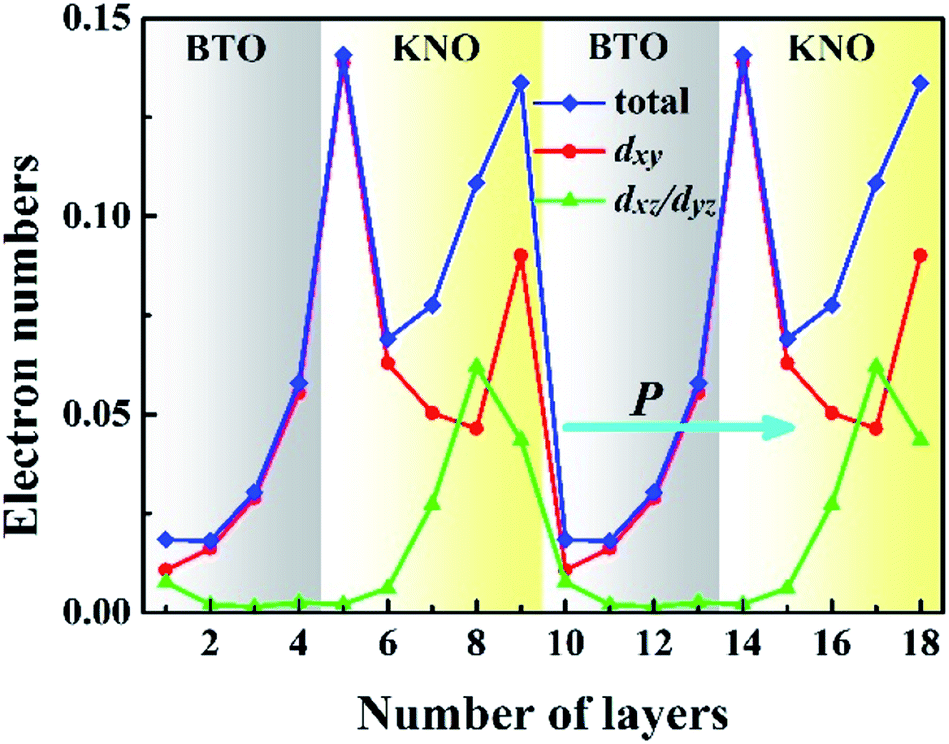 | ||
| Fig. 5 Calculated layer-resolved orbital electron distribution for each TiO2 (NbO2) layer in the NN-type SL. | ||
In addition, we calculated values of the bandgap Eg of BTO and KNO under different on-site Coulomb effective U parameter values, with results shown in Table S1.† The calculated layer-resolved partial DOS and 3D charge density for the NN-type SL when using U = 0 eV are plotted in Fig. S2,† while the calculated layer-resolved total orbital electrons for the NN-type SL with different U values are plotted in Fig. S3 in ESI.† We can clearly find that increasing the U values can increase the bandgap Eg of BTO and KNO, making it closer to the experimental band gap, but in fact, it has a slight influence on the layer-resolved electron distribution in the NN-type SL (Fig. S2 and S3†).
In conjunction with Fig. 2(a), when the ferroelectric displacement of an atomic layer dominantly occupied by the dxy states are slightly reduced, or even increased in few atomic layers (the NbO2 layer of the left interface in KNO region), while for atomic layers in which partially occupied by the dxz/dyz states, the ferroelectric displacement shows a rapid decrease, till nearly total disappearance (the NbO2 layer of the right interface in KNO region). Furthermore, in our calculations, the maximum numbers of electrons located at the NbO2 layer of the left and right interface in the KNO region (0.143 and 0.131 e−, respectively) are slightly larger than the reported 0.11 e−/(unit cell) of critical concentration for BTO-based ferroelectric.15 Incredibly, both are beyond the critical concentration, the ferroelectric displacement of the right interface with dxz/dyz states partially occupied is almost 0, yet the magnitude of polarization at left interface NbO2 layer with the dxy states fully occupied is not reduced but bigger than the reference value of bulk KNO, even though the electron density is slightly larger than the right interface NbO2 layer. The magnitude of polarization is reduced by dxz/dyz states having out-of-plane dispersion, while dxy states possessing in-plane dispersions do not have any influence to the polarization, which may be the reason why the magnitude of polarization is reduced and the polarization robustness is weakened for the NN-type SL, as shown in Fig. 2. Based on this fact, we can conjecture that the out-of-plane electrons are parallel to the polarization direction and thus can screen the net electric field to eliminate the local electric dipole, while in-plane electrons cannot eliminate the local electric dipole due to the fact that they are perpendicular to the polarization direction. In other words, in-plane electrons cannot screen out-of-plane polarization, which is why metallicity and ferroelectricity coexist in NN-type SLs.
To verify this inference, we calculated the ferroelectricity and metallicity of NN-type SLs with different thicknesses. Here, the thickness of KNO and BTO are n and m (n, m = 1, 2, 3, …), respectively, as shown in Fig. S4 in the ESI.† In Fig. S4(a),† the ferroelectricity gradually increases with increasing thickness n of KNO. When the SL thickness is small, the ferroelectricity disappears completely, which indicates that the ferroelectricity of the NN-type SL has a critical thickness. For example, for the KNO/BTO SL with n = 2 and m = 2 as shown in Fig. S4(b),† the number of dxz/dyz electrons is larger than that of dxy electrons, resulting in electric dipole being fully eliminated by the dxz/dyz electrons. When the layer number of the SL is sufficiently large, the ferroelectricity of the NN-type SL does not increase significantly as illustrated in Fig. S4(c).† Simultaneously, the metal states still exist in each unit cell and dxy electrons dominate, as shown in Fig. S4(d),† indicating that the in-plane dxy electrons have basically no effect on the out-of-plane polarization, and suggesting the metallicity of the NN-type SL may not having a critical thickness.
 | ||
| Fig. 6 Calculated layer-resolved partial DOS for PP-type SL, along with its charge density plot projected on the bands forming the metallic states, the energy range from 0 to 1 eV. | ||
To quantify the metallic state of each layer, we estimated their orbital hole numbers by integrating the partial DOS of unoccupied O 2p orbitals at each TiO2 (NbO2) layer for the PP-type SL, with results shown in Fig. 7. We can see that the hole carriers are symmetric in the BTO or KNO region when the intermediate atomic layer is used as a reference, indicating that the polarization has no effect on the distribution of hole carriers. Furthermore, the orbital-resolved orbital hole distribution intuitively displays that the px/py states having in-plane dispersion are absolutely unoccupied on all of the atomic layers, in combination with analysis of Fig. 2, there is no significant change in polarization and robustness in the PP-type SL, which further proves that the in-plane carriers cannot screen the out-of-plane polarization, hence, exhibiting quasi-two-dimensional p-type conductivity property in the PP-type SL. In addition, for the PP-type SL with n = 1 and m = 1 as shown in Fig. S5 in ESI,† the ferroelectricity does not disappear at the minimum thickness because px/py holes are still dominant, implying that the ferroelectricity of the PP-type SL has no critical thickness.
 | ||
| Fig. 7 Calculated layer-resolved orbital hole distribution for each TiO2 or NbO2 layer in the PP-type SL. | ||
3.3 Band alignment and band diagram
According to the polar catastrophe mechanism, in order to form a 2DEG at an interface between two insulating perovskite compounds, one prerequisite is that the conduction band minimum (Ec) of electron-acceptor must be lower than that of the electron-donor material.33,51 Similarity, to form a 2DHG, the necessary condition is that the valence band maximum (Ev) of the hole-acceptor oxide must be higher than that of the hole-donor material. However, 2DEG (2DHG) caused by polarization discontinuity does not need to consider the position of Ec (Ev) because carrier transfer is driven by an intrinsic electric field unless one of Ec (Ev) is much higher than the other.30To explore the formation mechanism of metallic states of each unit cell in the KNO/BTO SL, we calculated the total and partial DOS of bulk BTO and KNO by aligning their core energy levels of O 2s orbitals (the olive dashed line in Fig. 8(a)). The Ec (Ev) can be determined from the total DOS. The relative band alignments of the Ec (Ev) between the BTO and KNO are shown in Fig. 8(b), where we can find that both values of Ec and Ev of bulk BTO are higher than those of the bulk KNO. In Table S1 in ESI,† the calculated values of ΔEv, ΔEc, ΔEg between BTO and KNO at different U values indicate that ΔEv, ΔEc, ΔEg only change slightly when the U values increase. Therefore, by ignoring other factors and only looking from the position of bands at the interface, electrons will flow from the BTO region into the KNO region. The transfer of holes is exactly the opposite (as indicated by the pink and purple slim arrows in Fig. 8(b)). After reaching a temporary electrostatic equilibrium, the band diagrams for the KNO/BTO SL shown in Fig. 8(c) are formed on both sides of the interface, with upward band bending and downward band bending in BTO and KNO region, respectively, thus forming hole quantum well and electron quantum well. Note the shape changes of Ec and Ev as shown in Fig. 8(b and c). Based on this, we first consider the effect of polarization on carrier distribution. Generally speaking, when a ferroelectric material is combined with other materials, positive and negative charges are distributed in the head and tail terminals of polarization for ferroelectric materials (the middle illustration in Fig. 8(c)). Hence, electrons and holes are driven by polarization in the head terminal and tail terminal of polarization into other material, respectively (the pink and purple slim curved arrows in Fig. 8(c)). Yet since the values of both Ec and Ev of KNO are lower than those of BTO, at the right interface of KNO region, electrons return again whereas holes flow back into the left interface of BTO region (see the cyan and green slim curved arrows in Fig. 8(c)).
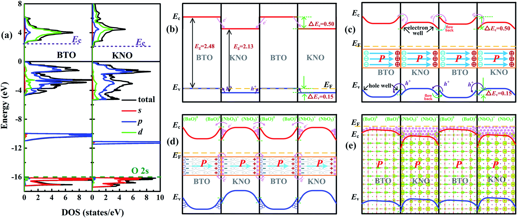 | ||
| Fig. 8 (a) Calculated total and partial DOS of bulk KNO and BTO, the DOS is aligned with respect to the O 2s state of the bulk BTO, the Ev of bulk BTO was set as reference (the zero of energy). (b) Band alignment of bulk KNO and BTO, (c) band diagram for a KNO/BTO SL before considering polarization, (d) band diagram for NN-type SL after considered polarization, (e) the final band diagram for NN-type SL. The orange dashed line, the red and blue thick solid line represent EF, Ec, and Ev, separately. The pink and purple slim arrows represent the direction of electrons (pink solid circles) and holes (blue hollow circles) transfer, respectively, and light blue thick straight arrow indicates the direction of polarization. The green thin straight arrows represent the polarization of atomic layers, and its length is proportional to the magnitude of the displacement. | ||
For a specific SL, the interfacial configuration needs to be considered. The band diagram for a NN-type SL after the discussed polarization effect is shown in Fig. 8(d). A large amount of electrons accumulate in the electron quantum well at the interface of the KNO region and a large number of holes accumulate in the quantum well at the interface of the BTO region. It was previously mentioned that for polar catastrophe mechanism to produce a 2DEG, it requires a minimum of Ec for nonpolar material. Therefore, it seems that the polar/nonpolar (NbO2)+/(BaO) interface of the NN-type SL may not be able to generate a 2DEG. However it is not the case since there is a small difference of in the value of Ec between BTO and KNO, many electrons accumulate at the interface of the KNO region, and it is easy for these electrons to occupy the energy level much higher than the Ec of BTO. Thus, the electrons caused by the polar discontinuity are easily and directly transferred into the conduction bands of BTO (as indicated by the slim curved arrows in Fig. 8(d)). Electrons are first completely recombined with holes at the interface of BTO, and then the remaining electrons continually transfer into the BTO region until about 0.5 e− transfer is completed. Electrons transferred to the interface of the BTO region occupy high conduction bands, turning the original upward band bending into downward band bending (notice the change of Ec (Ev) shown in Fig. 8(d and e)). The downward bending of the macroscopic averaged electrostatic potential at the interface can confirm this inference in Fig. S6 in ESI.† The polarization induced holes are fully recombined with part of electrons generated by the polar/nonpolar interface. This is the reason why the total electron number is 1 in our calculation and why we think that carriers are fully induced by the polar discontinuity rather than the polarization discontinuity.
Here, we need to clarify that there are two parts of unstable electrons in our NN-type SL, i.e., the electrons induced by the polar discontinuity and those by the polarization discontinuity concentrating at the left and right interfaces of BTO and KNO, respectively, which forms a temporary 2DEG at the interface. Hence, electrons occupy higher conduction bands need to move to lower conduction bands to achieve electrostatic equilibrium. Moreover, electrons in the left interface of the BTO or KNO region would drift to the right interface driven by the polarization electric field (the direction of electron increase in Fig. 5 is consistent with the direction of polarization in Fig. 8(d)). Simultaneously, owing to the fact Ec of the KNO is lower than that of the BTO, most of the electrons at the interface of BTO region reflow into the interface of the KNO region (electrons are mainly distributed in the interface of the KNO region in Fig. 5, also see the 3D electron density of the NN-type SL as the background image in Fig. 8(e)). The system reaches an electrostatic equilibrium when the polarization electric field can no longer drive the electron flow. In other words, the highest occupied conduction bands (EF in Fig. 8(e)) of BTO and KNO regions align with each other. The polarization electric field plays an important role in the redistribution of electrons throughout the whole system, especially for the dxz/dyz state electrons. The polarization electric field drives the distribution of dxz/dyz state electrons toward the right of interface of the KNO region. This in turn eliminates partial local electric dipoles to reduce the polarization (as indicated by the length of the green arrow that rapidly decreases as shown in Fig. 8(d)). The presence of electrons also can affect the spatial distribution of ferroelectric distortions, due to the fact that positive and negative charges are distributed in the head and tail terminals of polarization. As a consequence, these existing electrons will enhance the negative charge of the left interface and screen the positive charge of the right interface in BTO or KNO region, specifically enhancing the displacement at the left interface of KNO.
For the PP-type SL, the band diagram is shown in Fig. S7(a–c) in ESI.† Because the value of Ev of KNO is slightly smaller than that of BTO, holes are easily transferred to the BTO regions and most of the holes are distributed in the BTO region. In addition, since holes are almost entirely contributed by px/py states, they cannot be driven by the intrinsic electric field, and thus are approximately symmetrically distributed along with intermediate atomic layer in BTO or KNO region.
4 Conclusions
The ferroelectric polarization and crystal conductivity of two mainly canonical symmetric interface models of KNO/BTO SLs were investigated by first-principle electronic structure calculations. Different spatial distributions of ferroelectric distortions and quasi-two-dimensional conductive characteristics are shown in two symmetric interface models, indicating that they should belong to polar metals. For NN-type KNO/BTO SLs, electron carriers are mostly contributed by dxy states (in-plane dispersion) of Ti (Nb) atoms of TiO2 (NbO2) layers. At the same time, due to the presence of a small amount of dxz/dyz state electrons (out-of-plane dispersion), the magnitude of polarization is reduced and the polarization robustness is weakened. While for symmetric KNO/BTO SLs, hole carriers are almost contributed by occupied px/py states (in-plane dispersion) of O atoms of TiO2 (NbO2) layers, therefore, the magnitude of polarization and polarization robustness have not changed. Hence, the relationship between carrier and polarization reveals that the anisotropic coexistence of in-plane carrier and out-of-plane polarization is the key to achieve polar metals.In summary, the relationship between the polarization intensity and conductivity of the interfacial or non-interfacial layer versus the type of interface was elucidated through the band diagram in this paper. Based on our calculations, we can surmise that in order to realize a two-dimensional polar metal in a SL composed of two insulating perovskites, three conditions need to be met: (i) at least one material is ferroelectrics to provide polarization, (ii) at least one material is polar perovskite or Mott insulator to produce a 2DEG or a 2DHG, (iii) finally and most critically, the difference in Ec or Ev between two insulating materials is the smaller the better, so that EF can easily cross Ec or Ev of all materials. This work provides a clear picture for the realization of polar metals in the ferroelectric-based perovskite SL with the polar/nonpolar interface.
Conflicts of interest
The authors declare no competing financial interest.Acknowledgements
The authors would like to thank the financial support from the National Natural Science Foundation of China under Grant No. 11835008 and 51872250, and 61804130, the National Key R&D Program of China under Grant No. 2017YFF0105000, the Provincial Natural Science Foundation of Hunan under Grant No. 2018JJ4037 and 2018JJ2080, the Foundation of Innovation Center of Radiation Application (KFZC2018040201) and the State Key Laboratory of Intense Pulsed Radiation Simulation and Effect (Northwest Institute of Nuclear Technology) under Grant No. SKLIPR1606 and SKLIPR1814, and Hunan Provincial Innovation Foundation for Postgraduate Grant No. CX2017B280.References
- M. E. Lines and A. M. Glass, Principles and Applications of Ferroelectrics and Related Materials, Oxford Univ. Press, 2001 Search PubMed.
- P. W. Anderson and E. I. Blount, Phys. Rev. Lett., 1965, 14, 217 CrossRef CAS.
- Y. Shi, Y. Guo, X. Wang, A. J. Princep, D. Khalyavin, P. Manuel, Y. Michiue, A. Sato, K. Tsuda, S. Yu, M. Arai, Y. Shirako, M. Akaogi, N. Wang, K. Yamaura and A. T. Boothroyd, Nat. Mater., 2013, 12, 1024 CrossRef CAS.
- G. Giovannetti and M. Capone, Phys. Rev. B: Condens. Matter Mater. Phys., 2014, 90, 195113 CrossRef.
- D. Puggioni, G. Giovannetti, M. Capone and J. M. Rondinelli, Phys. Rev. Lett., 2015, 115, 087202 CrossRef.
- G. Giovannetti, D. Puggioni, J. M. Rondinelli and M. Capone, Phys. Rev. B, 2016, 93, 115147 CrossRef.
- S. Lei, M. Gu, D. Puggioni, G. Stone, J. Peng, J. Ge, Y. Wang, B. Wang, Y. Yuan, K. Wang, Z. Mao, J. M. Rondinelli and V. Gopalan, Nano Lett., 2018, 18, 3088 CrossRef CAS.
- Y. Mochizuki, Y. Kumagai, H. Akamatsu and F. Oba, Phys. Rev. Mater., 2018, 2, 125004 CrossRef CAS.
- D. Puggioni and M. Rondinelli, Nat. Commun., 2014, 5, 3432 CrossRef.
- T. H. Kim, D. Puggioni, Y. Yuan, L. Xie, H. Zhou, N. Campbell, P. J. Ryan, Y. Choi, J.-W. Kim, J. R. Patzner, S. Ryu, J. P. Podkaminer, J. Irwin, Y. Ma, C. J. Fennie, M. S. Rzchowski, X. Q. Pan, V. Gopalan, J. M. Rondinelli and C. B. Eom, Nature, 2016, 533, 68 CrossRef CAS.
- P. S. Halasyamani and K. R. Poeppelmeier, Chem. Mater., 1998, 10, 2753 CrossRef CAS.
- N. A. Benedek and T. Birol, J. Mater. Chem. C, 2016, 4, 4000 RSC.
- T. Kolodiazhnyi, M. Tachibana, H. Kawaji, J. Hwang and E. Takayama-Muromachi, Phys. Rev. Lett., 2010, 104, 147602 CrossRef CAS.
- F. Cordero, F. Trequattrini, F. Craciun, H. T. Langhammer, D. A. B. Quiroga and P. S. Silva Jr, Phys. Rev. B, 2019, 99, 064106 CrossRef CAS.
- Y. Wang, X. Liu, J. D. Burton, S. S. Jaswal and E. Y. Tsymbal, Phys. Rev. Lett., 2012, 109, 247601 CrossRef.
- K. Page, T. Kolodiazhnyi, T. Proffen, A. K. Cheetham and R. Seshadri, Phys. Rev. Lett., 2018, 101, 205502 CrossRef.
- S. Raghavan, J. Y. Zhang, O. F. Shoron and S. Stemmer, Phys. Rev. Lett., 2016, 117, 037602 CrossRef PubMed.
- X. Jing, W. Xu, C. Yang, J. Feng, A. Zhang, Y. Zeng, M. Qin, M. Zeng, Z. Fan, J. Gao, G. Zhou, X. Lu and J.-M. Liu, Appl. Phys. Lett., 2017, 110, 182903 CrossRef.
- C. Ma, K. J. Jin, C. Ge and G. Z. Yang, Phys. Rev. B, 2018, 97, 115103 CrossRef CAS.
- Y. Cao, Z. Wang, S. Y. Park, Y. Yuan, X. Liu, S. M. Nikitin, H. Akamatsu, M. Kareev, S. Middey, D. Meyers, P. Thompson, P. J. Ryan, P. Shafer, A. N'Diaye, E. Arenholz, V. Gopalan, Y. Zhu, K. M. Rabe and J. Chakhalian, Nat. Commun., 2018, 9, 1547 CrossRef.
- A. Ohtomo and H. Y. Hwang, Nature, 2004, 427, 423 CrossRef CAS.
- A. D. Caviglia, S. Gariglio, N. Reyren, D. Jaccard, T. Schneider, M. Gabay, S. Thiel, G. Hammerl, J. Mannhart and J. M. Triscone, Nature, 2008, 456, 624 CrossRef CAS.
- N. Reyren, S. Thiel, A. D. Caviglia, L. F. Kourkoutis, G. Hammerl, C. Richter, C. W. Schneider, T. Kopp, A. S. Rüetschi, D. Jaccard, M. Gabay, D. A. Muller, J.-M. Triscone and J. Mannhart, Science, 2007, 317, 1196 CrossRef CAS.
- A. Brinkman, M. Huijben, M. Van Zalk, J. Huijben, U. Zeitler, J. C. Maan, W. G. van der Wiel, G. Rijnders, D. H. A. Blank and H. Hilgenkamp, Nat. Mater., 2007, 6, 493 CrossRef CAS.
- S. Thiel, G. Hammerl, A. Schmehl, C. W. Schneider and J. Mannhart, Science, 2006, 313, 1942 CrossRef CAS.
- L. Weston, X. Y. Cui, S. P. Ringer and C. Stampfl, Phys. Rev. Lett., 2014, 113, 186401 CrossRef CAS.
- R. Pentcheva and W. E. Pickett, Phys. Rev. B: Condens. Matter Mater. Phys., 2006, 74, 035112 CrossRef.
- N. Nakagawa, H. Y. Hwang and D. A. Muller, Nat. Mater., 2006, 5, 204 CrossRef CAS.
- H. Lee, N. Campbell, J. Lee, T. J. Asel, T. R. Paudel, H. Zhou, J. W. Lee, B. Noesges, J. Seo, B. Park
![[thin space (1/6-em)]](https://www.rsc.org/images/entities/char_2009.gif) , L. J. Brillson, S. H. Oh, E. Y. Tsymbal, M. S. Rzchowski and C. B. Eom, Nat. Mater., 2018, 17, 231 CrossRef CAS.
, L. J. Brillson, S. H. Oh, E. Y. Tsymbal, M. S. Rzchowski and C. B. Eom, Nat. Mater., 2018, 17, 231 CrossRef CAS. - J. Cheng and K. Yang, J. Mater. Chem. C, 2018, 6, 6680 RSC.
- Y. Wang, W. Tang, J. Cheng, M. Behtash and K. Yang, ACS Appl. Mater. Interfaces, 2016, 8, 13659 CrossRef CAS.
- S. Nazir and K. Yang, ACS Appl. Mater. Interfaces, 2014, 6, 22351 CrossRef CAS.
- K. Yang, S. Nazir, M. Behtash and J. Cheng, Sci. Rep., 2016, 6, 34667 CrossRef CAS.
- J. Biscaras, N. Bergeal, A. Kushwaha, T. Wolf, A. Rastogi, R. C. Budhani and J. Lesueur, Nat. Commun., 2010, 1, 89 CrossRef CAS.
- P. Moetakef, J. R. Williams, D. G. Ouellette, A. P. Kajdos, D. Goldhaber-Gordon, S. J. Allen and S. Stemmer, Phys. Rev. X, 2012, 2, 021014 Search PubMed.
- H. Zhang, H. Zhang, X. Yan, X. Zhang, Q. Zhang, J. Zhang, F. Han, L. Gu, B. Liu, Y. Chen, B. Shen and J. Sun, ACS Appl. Mater. Interfaces, 2017, 9, 36456 CrossRef CAS.
- J. Cheng, S. Nazir and K. Yang, ACS Appl. Mater. Interfaces, 2016, 8, 31959 CrossRef CAS.
- Y. Chen, F. Trier, T. Kasama, D. V. Christensen, N. Bovet, Z. I. Balogh, H. Li, T. S. T. Karl, W. Zhang, S. Yazdi, P. Norby, N. Pryds and S. Linderoth, Nano Lett., 2015, 15, 1849 CrossRef CAS.
- S. Nazir, J. Cheng and K. Yang, ACS Appl. Mater. Interfaces, 2015, 8, 390 CrossRef.
- Y. Wang, M. K. Niranjan, S. S. Jaswal and E. Y. Tsymbal, Phys. Rev. B: Condens. Matter Mater. Phys., 2009, 80, 165130 CrossRef.
- K. D. Fredrickson and A. A. Demkov, Phys. Rev. B: Condens. Matter Mater. Phys., 2015, 91, 115126 CrossRef.
- N. Kumada, T. Kyoda, Y. Yonesaki, T. Takei and N. Kinomura, Mater. Res. Bull., 2007, 42, 1856 CrossRef CAS.
- M. B. Smith, K. Page, T. Siegrist, P. L. Redmond, E. C. Walter, R. Seshadri, L. E. Brus and M. L. Steigerwald, J. Am. Chem. Soc., 2008, 130, 6955 CrossRef CAS.
- W. Kleemann, F. J. Schäfer and M. D. Fontana, Phys. Rev. B: Condens. Matter Mater. Phys., 1984, 30, 1148 CrossRef CAS.
- H. H. Wieder, Phys. Rev., 1955, 99, 1161 CrossRef CAS.
- G. Kresse and J. Furthmüller, Phys. Rev. B: Condens. Matter Mater. Phys., 1996, 54, 11169 CrossRef CAS.
- G. Kresse and D. Joubert, Phys. Rev. B: Condens. Matter Mater. Phys., 1999, 59, 1758 CrossRef CAS.
- J. P. Perdew, K. Burke and M. Ernzerhof, Phys. Rev. Lett., 1996, 77, 3865 CrossRef CAS.
- L. Wang, T. Maxisch and G. Ceder, Phys. Rev. B: Condens. Matter Mater. Phys., 2006, 73, 195107 CrossRef.
- V. I. Anisimov, J. Zaanen and O. K. Andersen, Phys. Rev. B: Condens. Matter Mater. Phys., 1991, 44, 943 CrossRef CAS.
- A. Giampietri, G. Drera and L. Sangaletti, Adv. Mater. Interfaces, 2017, 4, 1700144 CrossRef.
Footnotes |
| † Electronic supplementary information (ESI) available. See DOI: 10.1039/c9ra06209b |
| ‡ Gang Li and Huiyu Huang are the co-first authors. |
| This journal is © The Royal Society of Chemistry 2019 |