
 Open Access Article
 This Open Access Article is licensed under a Creative Commons Attribution-Non Commercial 3.0 Unported Licence
Probing the properties of lattice vibrations and surface electronic states in magnetic semiconductor CrPS4†
Hongbiao
Wu
and
Haiping
Chen
*
School of Mechanics and Optoelectronic Physics, Anhui University of Science and Technology, Huainan 232001, P. R. China. E-mail: hpchen01@mail.ustc.edu.cn
First published on 30th September 2019
Abstract
Searching for multifunctional materials with magnetism and semiconductivity is one of the goals of research into two-dimensional (2D) systems. Herein, we report a chemical vapor transport method to successfully synthesize a layered magnetic semiconductor, CrPS4. Under parallel and perpendicular polarization configurations, the anisotropic optical response of the (001) surface was investigated by polarized Raman spectroscopy; the Raman peak intensity was recorded with the crystal rotated from 0° to 360°, taking the symmetry of the Raman tensor into account; the A or B vibrational mode of different Raman peaks can be clearly distinguished. Moreover, the electronic state of the (001) single-crystal surface was investigated by ultraviolet photoelectron spectroscopy (UPS), which reveals the valence band position and work function of the (001) surface.
Introduction
Light-matter interaction is one of the most important tools to investigate the properties of matter, especially for the characterization of competition or cooperation phenomena of collectively ordered electronic states in various two-dimensional (2D) systems. Similar to the linear dispersion energy band in graphene, Dirac electrons in line-node semimetal ZrSiS have been confirmed by optical conductivity behaviour, which exhibits a flat optical conductivity in a wide frequency range from 250 to 2500 cm−1 (30–300 meV), and this unusual frequency-independent conductivity is assigned to interband transitions between Dirac bands near the Fermi level.1Recently, a two-dimensional CrPS4 single crystal was systematically investigated for their electronic, magnetic, and thermal transport properties and density functional theory computation.2–10 In this work, the lattice vibration and surface electronic states of the (001) surface are systematically investigated by polarized Raman spectroscopy and ultraviolet photoelectron spectroscopy (UPS). Parallel and perpendicular Raman scattering technique is used to investigate the anisotropic optical response of the (001) crystal surface, combined with nuclear site group analysis; the Raman peaks can be assigned to A or B vibrational modes. Moreover, the electronic structure of the (001) surface is detected by ultraviolet photoelectron spectroscopy (UPS), from which the work function for the (001) surface can be deduced.
Experiment and characterization
Preparation of single-crystal CrPS4
A CrPS4 single crystal was synthesized by a chemical vapor transport method. Stoichiometric amounts of Cr powder, red P powder and S powder in a mole ratio of 1![[thin space (1/6-em)]](https://www.rsc.org/images/entities/char_2009.gif) :1:4 were weighed and loaded into a silica tube, which was sealed under high vacuum. The sealed silica tube was placed in a two-zone tube furnace for 7 days with the hot side at 650 °C and the cold side at 550 °C, which were subsequently cooled to room temperature.
:1:4 were weighed and loaded into a silica tube, which was sealed under high vacuum. The sealed silica tube was placed in a two-zone tube furnace for 7 days with the hot side at 650 °C and the cold side at 550 °C, which were subsequently cooled to room temperature.
Structure and polarized Raman scattering measurements
X-ray Laue diffraction was carried out using a PANalytical X'Pert MPD PRO system in the Bragg–Brentano geometry (240 mm radius) with Cu-Kα radiation (Cu Kα1 = 1.54056 Å) to characterize the crystal structure. A Horiba Raman spectrometer (XPLORA-ONE) equipped with a microscope was used to image the sample (50×). For parallel and perpendicular Raman experiments, a large single-crystal (14 mm × 6 mm) was put onto a scotch tape, which was pasted with another scotch tape over and over for 8–12 times; then, the samples were transferred onto a silicon substrate with marked points and singled out for Raman experiments (shown in top right-hand corner of Fig. 2, about 20 μm × 8 μm), and the crystal was obtained with exposed (001) crystal facets. A Horiba Raman microscope (XPLORA-ONE) was used to collect Raman spectra, which was dispersed by a 1200 grooves per mm diffraction grating. The incident 532 nm laser within 1.5 mW was focused by a 50× objective lens, and the spot size of the laser was about 1 μm. A polarizer was inserted in the optical path of the scattered light, so that parallel or perpendicular polarized light relative to the input polarization can be selected.Results and discussion
Fig. 1a shows the X-ray Laue diffraction pattern of the obtained single-crystal CrPS4, which is consistent with JCPDF file (monoclinic, C3 2 (#5), a = 10.87 Å, b = 7.25 Å and c = 6.14 Å). The diffraction peaks indicate that the CrPS4 single crystal is stacked layer by layer along the c-axis. The schematic atomic structure model is exhibited in Fig. 1b and c; Fig. 1b illustrates single-layer CrPS4, where there is a distorted octahedral CrP6 group with six neighbouring S atoms and a PS4 tetrahedron cluster with four neighbouring S atoms, which is viewed from the c-axis in a single layer, and Fig. 1c shows that a chain of distorted CrS6 octahedra is bridged by P atoms. | ||
| Fig. 1 Structural characterization of layered CrPS4: (a) X-ray Laue diffraction pattern, and (b) and (c) atomic structure model. | ||
According to the structural characterization in Fig. 1, layered CrPS4 crystallizes in the monoclinic phase (C3 2, no. 5). There are 12 atoms in the primitive unit cell, leading to 33 optical and 3 acoustic phonon branches in the Brillouin zone centre, and nuclear site group theory reveals that all the vibrational modes in the zone centre can be described as: 17A⊕19B, in which only A⊕2B are the acoustic phonon branches, the rest are optical phonon branches and Raman active modes. The Raman scattered intensity can be expressed as  where
where  and
and  are the unit polarization directions of scattered and incident light, respectively,11,12 and
  is the second-rank Raman tensor, which is given below in the CrPS4 crystal coordinate system:

Experimentally, the angle-dependent Raman test was performed as follows: the incident 532 nm laser propagates along the Z-axis and is polarized along a fixed X-axis direction of the laboratory coordinate system, which remains unchanged in the experimental process. The anisotropic Raman scattering intensity of the (001) surface was measured by rotating the single crystal around the Z-axis in 10° steps, in order to sign the rotating angle of the sample. In Fig. 2, the red vector is fixed on the sample and rotated with the sample in the XY plane; θ represents the angle between the X-axis and the red axis, which signs the rotating angle of the sample.
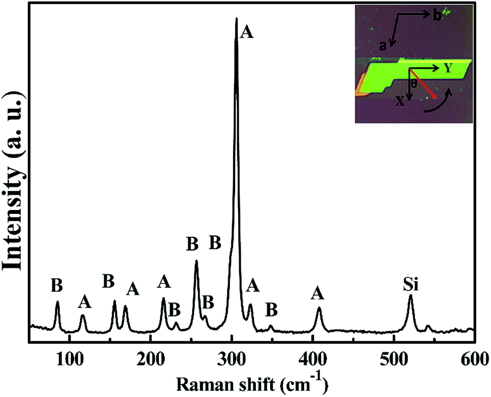 | ||
| Fig. 2 Unpolarized Raman spectrum of layered CrPS4; schematic Raman scattering configuration is shown on the top right-hand corner. The red vector fixed on the sample is rotated in the XY plane, θ represents the angle between the X-axis and the red axis, which is also the rotating angle, and the arc with arrow signs the rotating direction of the sample. | ||
Theoretically, to obtain the evolution rule of the anisotropic Raman scattering intensity, we need to reformulate the form of Raman tensors in the laboratory frame XYZ, in which the c-axis of the crystal coincides with the Z-axis. The backscattered light propagates along the Z-axis and is collected by the polarizer along the X-axis (Y-axis), which corresponds to parallel (perpendicular) polarization, and thus, in the laboratory frame XYZ, the Raman tensor can be described as:

| αXX = αxxcos2θ + αxysin2θ + αyysin2θ |
| αXY = −αxxsinθcosθ + αxy(cos2θ − sin2θ) + αyysinθcosθ |
Under parallel polarization configuration, the Raman scattering intensity scales with |αXX|2, while under perpendicular scattering condition, the Raman peak intensity scales with |αXY|2. In summary, the angle-dependent Raman optical response for A and B modes under parallel and perpendicular polarizations is given in Table 1.
| Raman modes | Scattering configurations | |
|---|---|---|
| Angle dependence of Raman intensities | ||
| Parallel
|
Perpendicular
|
|
| A | |acos2θ + csin2θ|2 |
|(c − a)sinθcosθ|2 |
| B | |esin2θ|2 |
|ecos2θ|2 |


From Table 1, the angle-dependent Raman peak intensity for B mode exhibits antiphase oscillation at different scattering configurations. Fig. 3a and b shows that at parallel polarization, the intensities for seven Raman shifts located at 84.8 cm−1, 155.3 cm−1, 231.3 cm−1, 257.1 cm−1, 266.9 cm−1, 298.4 cm−1, and 348.3 cm−1 are out of phase with those at perpendicular polarization in Fig. 3c and d, in order to quantitatively describe the experimental results. For each angle-dependent Raman peak from 0° to 360° in 10° steps, with the strongest Raman peak as a criterion, the peak intensity is normalized, and all seven bands are normalized and fall within the error bar, which are respectively exhibited in Fig. 4a and b for parallel and perpendicular polarization (the angle-dependent intensity evolution from 180° to 360° is shown in ESI Fig. 1e and h†), so that the seven Raman shifts can be assigned to the B vibrational mode.
 | ||
| Fig. 3 Angle-dependent Raman peak intensity for the (001) surface with the crystals rotated in 10° steps: (a) and (b) parallel polarization, and (c) and (d) perpendicular polarization. | ||
 | ||
| Fig. 4 The relationship between normalized intensity and rotating angle for the observed Raman peaks under parallel and perpendicular polarization configurations is shown in (a–e), the theoretical formula is fitted and given in red curve. | ||
Theoretically, the Raman scattering intensity for the A mode is related to two Raman tensor elements, and the angle-dependent optical Raman response of the (001) surface is expected to be more diverse. For the 116.7 cm−1 Raman shift, the Raman peak intensity evolution as a function of the angle shows the appearance of “M” at parallel geometry, as shown in Fig. 4e; furthermore, the ratio of Raman tensor c to a, which is fitted to the experimental values at parallel polarization, is 1.2. In contrast, at perpendicular geometry, the intensity evolution is shown in Fig. 4b; it can be deduced that the peak at 116.7 cm−1 belongs to the A mode. The same situation occurs for the Raman peak at 216.0 cm−1, the only difference being that at perpendicular polarization, the Raman peak intensity is quite weak, and we cannot detect how it changed. However, we can still infer that the 216.0 cm−1 Raman shift is classified under the A mode. Fig. 4c and d show the angle-dependent Raman response for 168.8 cm−1 at parallel and perpendicular polarization geometries, respectively; the fitted ratio of Raman tensor c to a is 1/7, and there is no doubt that the Raman peak at 168.8 cm−1 belongs to the A mode. The strongest Raman peak at 305.6 cm−1 shows oscillation with π phase at parallel and perpendicular polarization geometries, as shown in Fig. 4c. In addition, compared with parallel polarization, the intensity evolution as a function of the angle has a small phase difference at the perpendicular geometry and the intensity evolution period π contradicts with the theoretical value π/2, and hence, we speculate that the intensity of the Raman peak at 305.6 cm−1 is influenced by a nearby Raman peak at 298.4 cm−1. The Lorentz function is used to fit Raman peaks at 298.4 cm−1 and 305.4 cm−1 at the perpendicular polarization geometry, and the angle-dependent Raman peak at 305.4 cm−1 almost exhibits the π phase, which is shown in ESI Fig. 2.† This unusual optical response can be traced back to other origin, combined with Table 1, we still assume that the Raman peak at 305.6 cm−1 belongs to A mode. Fig. 4c also displays the oscillation period of Raman peaks at 323.2 cm−1 and 407.8 cm−1 at the parallel polarization geometry. However, from Fig. 3c and d, owing to the weak Raman peak intensity at the perpendicular polarization geometry, we cannot distinguish the intensity evolution rule, and the two Raman peaks most likely belong to the A mode. In summary, combined polarized optical Raman experiment and group theory analysis can help us determine the vibrational modes of Raman peaks in layered magnetic semiconductor CrPS4.
Ultraviolet photoelectron spectroscopy (UPS) was used to determine the valence band position (equivalent to ionization potential) and work function of the (001) surface of the single-crystal CrPS4. The experimental parameters were set as follows: the excitation energy of synchrotron radiation was 168.5 eV, the additional bias was 10 V, and work function of the instrument was 3.76 eV. The valence band position of the (001) surface was determined according to the equation: Φ = hν − ΔE, where ΔE is the binding energy difference between the secondary electron cut-off and the valence band maximum, and Φ was calculated to be 8.2 eV. According to the previous density functional theory result,2 based on the assumption that the energy level of the band gap center is independent of the functionals used, the calculated valence band-edge energy level of single-layer CrPS4 was determined to be 6.95 eV, and the theoretical and experimental results were qualitatively consistent. The work function of the (001) surface was obtained by subtracting the binding energy of the secondary electron cut-off from the excitation energy and calculated to be 3.84 eV (Fig. 5).
 | ||
| Fig. 5 UPS spectra characterization of the electronic structure of the (001) surface for bulk CrPS4. The dashed lines mark the tangents of the curve and the baseline, the intersections of the left and right tangents with the baseline, respectively, give the valence band maximum and edge of secondary electron cut-off. | ||
Conclusions
In summary, a highly crystallized magnetic semiconductor, CrPS4, has been fabricated by the chemical vapor transport method. By the polarized Raman optical experiment in a backscattering way, the observed Raman peaks can be classified into A or B phonon mode. UPS reveals the valence band position and work function, which are qualitatively consistent with the previous density functional theory.Conflicts of interest
There are no conflicts to declare.Acknowledgements
This work is supported by Natural Science Foundation of China (51502005, 51602005, 11647001 and 11404005), Key Foundation for Young Talents in College of Anhui Province (gxyqZD2016081, 2013SQRL026ZD).References
- B. Schilling, L. M. Schoop, B. V. Lotsch, M. Dressel and A. V. Pronin, Phys. Rev. Lett., 2017, 119, 187401 CrossRef.
- H. L. Zhuang and J. Zhou, Phys. Rev. B, 2016, 94, 195307 CrossRef.
- Q. L. Pei, X. Luo, G. T. Lin, J. Y. Song, L. Hu, Y. M. Zou, L. Yu, W. Tong, W. H. Song, W. J. Lu and Y. P. Sun, J. Appl. Phys., 2016, 119, 043902 CrossRef.
- A. Louisy, G. Ouvrard, D. M. Schleich and R. Brec, Solid State Commun., 1978, 28, 61 CrossRef CAS.
- S. Kim, J. Lee, G. Jin, M. Ho Jo, C. G. Lee and S. M. Ryu, Nano Lett., 2019, 19, 6 Search PubMed.
- J. H. Lee, T. Y. Ko, J. H. Kim, H. Y. Bark, B. G. Kang, S. G. Jung, T. S. park, Z. H. Lee, S. M. Ryu and C. G. Lee, ACS Nano, 2017, 11, 11 Search PubMed.
- M. W. Joe, J. H. Lee and C. G. Lee, Comput. Mater. Sci., 2019, 162, 277 CrossRef CAS.
- J. H. Lee, T. Y. Ko, J. H. Kim, H. Y. Bark, B. Y. Kang, S. G. Jung, T. S. park, Z. H. Lee, S. M. Ryu and C. G. Lee, ACS Nano, 2017, 11, 11 Search PubMed.
- M. J. Lee, S. K. Lee, S. M. Lee, K. B. Gan, C. S. Yoon, J. T. Jang, S. H. Kim, D. H. Kwon, M. Y. Kim, J. P. Ahn, D. H. Kim, J. G. Park and B. H. Park, NPG Asia Mater., 2018, 10, 23 CrossRef CAS.
- C. C. Mayorga-Martinez, Z. Sofer, D. Sedmidubsky, S. Huber, A. Y. S. Eng and M. Pumera, ACS Appl. Mater. Interfaces, 2017, 9, 12563 CrossRef CAS.
- J. X. Wu, N. N. Mao, L. M. Xie, H. Xu and J. Zhang, Angew. Chem., Int. Ed., 2015, 54, 2366–2369 CrossRef CAS.
- T. Sander, S. Eisermann, B. K. Meyer and P. J. Klar, Phys. Rev. B: Condens. Matter Mater. Phys., 2012, 85, 165208 CrossRef.
Footnote |
| † Electronic supplementary information (ESI) available. See DOI: 10.1039/c9ra05861c |
| This journal is © The Royal Society of Chemistry 2019 |