
 Open Access Article
 This Open Access Article is licensed under a Creative Commons Attribution-Non Commercial 3.0 Unported Licence
Induced growth of quasi-free-standing graphene on SiC substrates
Zhenxing
Liu
 a,
Zhen
Su
a,
Qingbo
Li
a,
Li
Sun
*a,
Xue
Zhang
a,
Zhiyuan
Yang
a,
Xizheng
Liu
b,
Yingxian
Li
ac,
Yanlu
Li
a,
Fapeng
Yu
*a and
Xian
Zhao
a
a,
Zhen
Su
a,
Qingbo
Li
a,
Li
Sun
*a,
Xue
Zhang
a,
Zhiyuan
Yang
a,
Xizheng
Liu
b,
Yingxian
Li
ac,
Yanlu
Li
a,
Fapeng
Yu
*a and
Xian
Zhao
a
aInstitute of Crystal Materials, Center for Optics Research and Engineering of Shandong University, Jinan 250100, P. R. China. E-mail: sdusunli@sdu.edu.cn; fapengyu@sdu.edu.cn
bTianjin Key Laboratory of Advanced Functional Porous Materials, Institute for New Energy Materials and Low-carbon Technologies, School of Materials Science and Engineering, Tianjin University of Technology, Tianjin 300384, P. R. China
cShandong Key Laboratory of Biophysics, Institute of Biophysics, Dezhou University, Dezhou 253023, P. R. China
First published on 10th October 2019
Abstract
Free-standing graphene grown on SiC substrates is desirable for micro- and nano-electronic device applications. In this work, an induced growth method to fabricate quasi-free-standing graphene on SiC was proposed, where graphene nucleation sites were generated on the SiC substrate and active carbon sources were subsequently introduced to grow graphene centered along the established nucleation sites. The structure and morphology of the cultivated graphene were characterized by using X-ray photoelectron spectroscopy (XPS), Raman spectroscopy, and high-resolution transmission electron microscopy (HRTEM). Compared to the traditional epitaxial growth methods on SiC substrates, this approach shows a significant reduction of the buffer layer. This study provides an efficient method for growing quasi-free-standing graphene on SiC substrates and is believed to be able to broaden the application of graphene in electronic devices as SiC is an intrinsically outstanding wide bandgap semiconductor.
1. Introduction
Graphene, a single atomic layer, 2-dimensional thin-film material, has been considered as the most promising material for next generation electronic devices due to its unique properties,1,2 such as ultrahigh intrinsic carrier mobility3 and room-temperature quantum Hall effects.4 Among the current methods in the fabrication of high-quality graphene for electronic device applications, the thermal decomposition of SiC (epitaxial growth method) has shown the most potential in obtaining wafer-scale and high-quality graphene materials.5 Compared with the chemical vapor deposition (CVD) method using a catalytic substrate (Cu,6 Ni,7 and Pt8), the thermal decomposition of SiC directly deposits graphene on the insulating substrate.9 Hence, the chemical contaminants and defects introduced in the transfer step of the CVD method can be avoided and the intrinsic properties of graphene can be maintained.Current research of epitaxial graphene growth on SiC is mainly focused on the Si-face [the (0001) facet of the SiC substrate], since the graphitization on the Si-face of SiC wafers is more controllable and the grain size of graphene is larger in comparison with that prepared on the C-face [the (000![[1 with combining macron]](https://www.rsc.org/images/entities/char_0031_0304.gif) ) facet of the SiC substrate].10,11 SiC single crystal has an atomic step-shaped structure, which is not conducive to large scale graphene growth on these narrow step terraces, where wider terraces may offer better platforms. The hydrogen-etching (H-etching) process has proven to be an effective and environmentally-friendly method to broaden the step terraces as H2 can react with SiC terrace at the terrace edge area and the step-shaped structure can be reconstructed under high temperature. To achieve uniform terrace structure and high-quality graphene growth, H-etching is performed prior to the graphitization process to broaden the step terraces on the SiC substrate.12 Even with the advantages of the Si-face in epitaxial graphene growth, there is still a big challenge in obtaining free-standing graphene on the Si-face of the substrate, which is the so-called buffer layer (BL). The BL forms prior to the growth of the first layer graphene, which is partially covalently-bonded with the SiC substrate.13 The buffer layer leads to the disruption of the π-band electronic structure and degradation of the electron mobility, which is unfavorable in graphene-based applications.
) facet of the SiC substrate].10,11 SiC single crystal has an atomic step-shaped structure, which is not conducive to large scale graphene growth on these narrow step terraces, where wider terraces may offer better platforms. The hydrogen-etching (H-etching) process has proven to be an effective and environmentally-friendly method to broaden the step terraces as H2 can react with SiC terrace at the terrace edge area and the step-shaped structure can be reconstructed under high temperature. To achieve uniform terrace structure and high-quality graphene growth, H-etching is performed prior to the graphitization process to broaden the step terraces on the SiC substrate.12 Even with the advantages of the Si-face in epitaxial graphene growth, there is still a big challenge in obtaining free-standing graphene on the Si-face of the substrate, which is the so-called buffer layer (BL). The BL forms prior to the growth of the first layer graphene, which is partially covalently-bonded with the SiC substrate.13 The buffer layer leads to the disruption of the π-band electronic structure and degradation of the electron mobility, which is unfavorable in graphene-based applications.
To date, significant investigations have been performed to eliminate the BL effect. The commonly used method to decouple the interactions of graphene and the SiC substrate are intercalating various elements such as hydrogen,14 oxygen,15 silicon16 and fluorine.17 However, there are still some challenges, such as hydrogen desorbing at elevated temperatures leading to graphene transforming into a buffer layer again. For fluorine or oxygen intercalation, contaminants can be introduced to the pristine structure due to the extra elements. Some other methods have also been attempted to decouple the buffer layers. Hu et al.18 obtained near-free-standing epitaxial graphene by flash annealing at high temperature, and Bao et al.19 reported a similar method to obtain free-standing graphene via a rapid-cooling process using liquid nitrogen. Though the capability of buffer-free graphene growth was reported, the requirements for the equipment were stringent and the homogeneity of the obtained graphene was hard to control. Combining the advantages of the CVD and epitaxial growth methods is an effective means to prepare free-standing graphene on a SiC substrate, however, related studies are very rare20 and free-standing graphene is difficult to attain since the mechanism is not clear yet.
In this work, an induced growth method to cultivate graphene on SiC (0001) substrate was presented and quasi-free-standing high-quality graphene with low interfacial stress was reported. The structure and quality of the graphene were characterized by using X-ray photoelectron spectroscopy (XPS) and high resolution transmission electron microscope (HRTEM). Moreover, the contributions of the initial nucleation and the subsequent growth process were clarified, and the mechanism of induced graphene growth was studied.
2. Experimental section
The preparation of graphene on the Si-face (0001) of an on-axis 4H–SiC substrate was performed in a homemade high temperature chemical vapor deposition (HT-CVD) system. The substrates used in this study were 10 mm × 10 mm pieces prepared from a 3-inch semi-insulating SiC wafer. The SiC substrates were chemically cleaned in acetone and methanol to remove the surface contaminants, followed by etching in HF solution to wipe off the oxide on the SiC surface. The cleaned substrate was placed into the HT-CVD furnace, and the chamber was pumped to the low pressure of 1 × 10⁻⁵ mbar. The preparation procedures were divided into three steps: H-etching, nucleation, and growth, as described in Fig. 1(a–c). Firstly, the H-etching was processed in 800 mbar of H2 for 20 min at 1475 °C to broaden the width of the step terrace. After H-etching, the SiC substrate with uniform and flat terraces was obtained for high quality graphene growth. The substrate was then heated to 1650 °C for 3 min with an ambient pressure of 600 mbar (Ar) to build a condition feasible for carbon atom nucleation. After that, the growth step was executed at a temperature of 1450 °C under the pressure of 20 mbar for 5 min. Meanwhile, the CH4 was introduced as a carbon source for graphene growth centering around the established nucleation sites on the SiC substrate.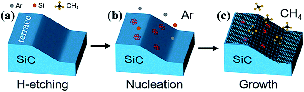 | ||
| Fig. 1 Schematic diagram of the graphene growth process on a SiC substrate: (a) H-etching, (b) nucleation, and (c) growth. | ||
As three steps (H-etching, nucleation and growth) were involved in the proposed method, comparative experiments were carried out to study the respective roles they played in this process. The detailed experimental procedures were summarized in Table 1, where different groups of samples named as A1, A2, A3, and A4 were prepared, as shown in Fig. 2. In contrast to the growth step, the epitaxial growth represented the graphitization of the SiC substrate itself, since the chamber was filled with inert Ar gas instead of CH4. For the A1 group samples, the substrate went directly into the growth step after H-etching, bypassing the nucleation step. The A2 group samples only proceeded through the H-etching and nucleation processes. Then they were cooled down to room temperature, bypassing the growth step. Different from the A2 group samples, the A3 group samples underwent all three procedures, but the graphene growth was supported by the SiC substrate itself rather than the introduced CH4 source. For comparison, the A4 group samples experienced all the induced growth procedures.
| H-etching | Nucleation | Epitaxial growth | Growth | |
|---|---|---|---|---|
| Atmosphere | H2 | Ar | Ar | CH4, H2 |
| Temperature | 1475 °C | 1650 °C | 1450 °C | 1450 °C |
| A1 | Yes | No | No | Yes |
| A2 | Yes | Yes | No | No |
| A3 | Yes | Yes | Yes | No |
| A4 | Yes | Yes | No | Yes |
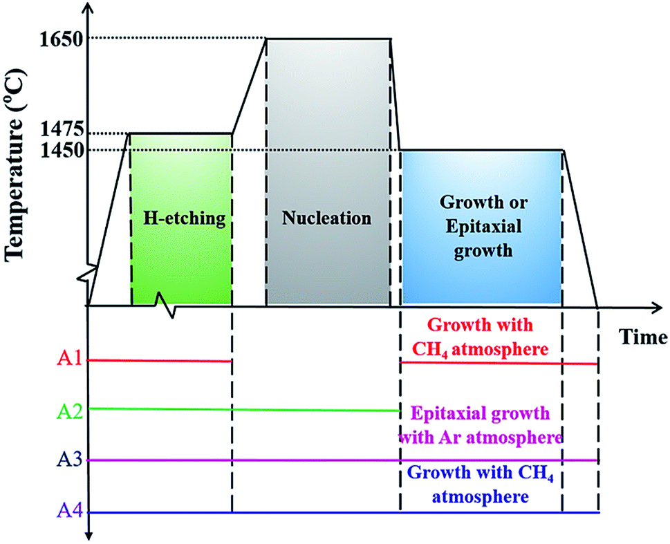 | ||
| Fig. 2 Schematic diagram of the graphene growth process of A1–A4 samples. | ||
The surface morphology characterization was conducted by an Atomic Force Microscope (AFM) from the Veeco Instruments Company, and the results were analyzed by using the NanoScope Analysis software. Raman measurements were utilized since it does not require any pretreatment, and the sample is not destroyed. Raman spectra were collected by an HR800 Raman spectrometer system from Horiba Jobin Yvon with a 532 nm wavelength laser (the numerical of the aperture is 0.90). The XPS was recorded by ESCALAB 250 software from Thermo Fisher Scientific. To improve the resolution, the Al Kα X-ray radiation in an ultra-high vacuum was monochromatized with a photon linewidth of 0.16 eV. The experimental data were processed in Thermo Avantage software, and the SiC component was fixed at around 283.5 eV, which was attributed to the carbon atoms of the SiC substrate. The HRTEM observation was performed on an FEI Talos F200X microscope at 200 kV. For quasi-free- standing graphene characterization, the HRTEM specimen was prepared in advance by a focused ion beam (FIB) on FEI Helios NanoLab 460HP and observed under scanning electron microscopy (SEM).
3. Results and discussion
The chemical composition of the prepared samples was characterized by XPS. Fig. 3(a–d) show the XPS C 1s spectra of A1, A2, A3, and A4, respectively. For making a comparison, the graphene sample prepared by conventional epitaxial growth (named as sample B) was also presented. The graphene growth method was the same as that described in the reported literature,21 and the corresponding XPS spectra were given in Fig. 3(e). The black solid curves in Fig. 3 are the experimental data, and the gray solid curves are the fitted results relevant to the components, SiC, graphene, C![[double bond, length as m-dash]](https://www.rsc.org/images/entities/char_e001.gif) O, S1, and S2. The peaks around ∼283.5 eV and ∼284.5 eV represent the SiC and graphene, respectively,22 and the remaining two components, S1 and S2, are related to the buffer layer. The S1 component is attributed to one-third of the carbon atoms in the buffer layer covalently bonded to the SiC substrate, and the S2 component results from the other two-thirds of the carbon atoms with the sp2 configuration in the buffer layer.23,24 Additionally, a minor contribution at high binding energy is attributable to the presence of CO,25,26 which might be formed during the process of graphitization,25 or related to the sample preparation process during the XPS test.
O, S1, and S2. The peaks around ∼283.5 eV and ∼284.5 eV represent the SiC and graphene, respectively,22 and the remaining two components, S1 and S2, are related to the buffer layer. The S1 component is attributed to one-third of the carbon atoms in the buffer layer covalently bonded to the SiC substrate, and the S2 component results from the other two-thirds of the carbon atoms with the sp2 configuration in the buffer layer.23,24 Additionally, a minor contribution at high binding energy is attributable to the presence of CO,25,26 which might be formed during the process of graphitization,25 or related to the sample preparation process during the XPS test.
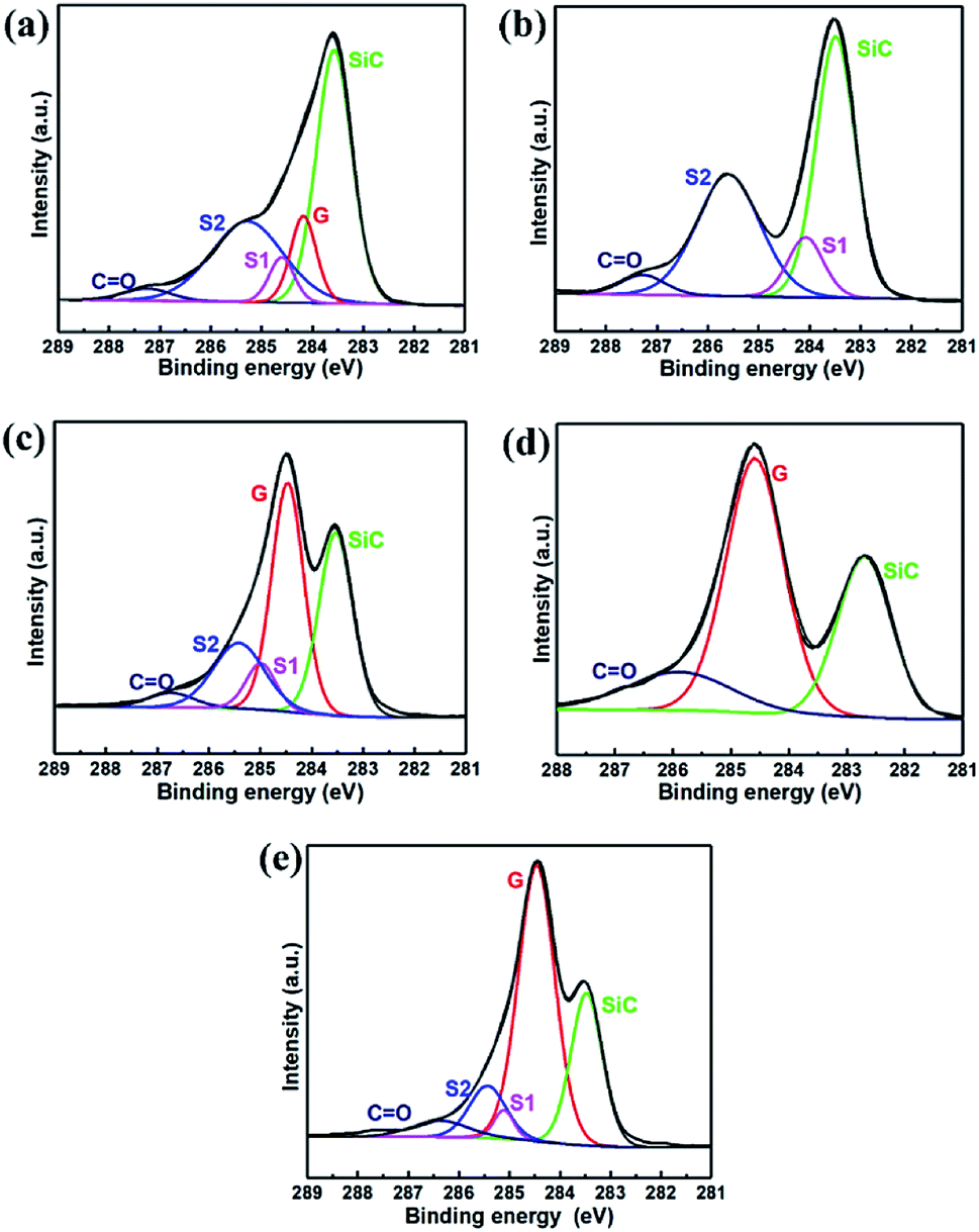 | ||
| Fig. 3 XPS C 1s spectra of (a) A1, (b) A2, (c) A3, (d) A4, and (e) B, respectively. Black solid curves are the experimental data and the gray solid curves are the envelope line of the fitted components (SiC, graphene, CO, S1, and S2). | ||
As depicted in Fig. 3(a), the XPS spectrum of the A1 sample consists of all four components, graphene, S1, S2, and SiC peaks. The intensity of graphene is similar to that of the buffer layer, which means the graphene was formed on the top of the SiC substrate and the buffer layer still exists at the interface. Taking the growth condition into consideration, the graphene was presumed to be formed randomly on the substrate by the decomposition of CH4. The buffer layer formation can be ascribed to the partial pyrolysis of the substrate during the growth process since Si atoms already sublimated at the temperature of 1450 °C.27 It was observed that the A2 sample consisted of three components (S1, S2, and SiC) in the spectrum, as presented in Fig. 3(b). The absence of the graphene component can be attributed to the missing graphene growth process. The S1 and S2 peaks indicated the individual nucleation step would also result in the formation of the buffer layer. For the A3 sample, the shape and location of the four component peaks in the XPS C 1s spectra [Fig. 3(c)] were found to be very similar to those of the sample prepared by the traditional epitaxial growth method, as shown in Fig. 3(e), indicating that in the epitaxial growth process, adding a nucleation step does not change the intrinsic growth mechanism. Based on the above comparative experiments, it was observed that the exclusive step of nucleation or growth did not reduce the formation of the buffer layer. However, the A4 sample that underwent the complete induced growth process exhibited symmetric SiC and graphene components [Fig. 3(d)]. Moreover, it was noted that the energy difference between SiC and graphene is about 2 eV, which is consistent with the same property of quasi-freestanding graphene.24,28 The shift of the SiC peak to lower binding energy may be caused by band bending,28 and further study is needed. The comparative results proved that the proposed induced growth method could reduce the formation of buffer layer structure effectively.
More detailed investigations were executed on the graphene prepared by the proposed induced growth method. The surface morphologies of the Si-face substrate were depicted in Fig. 4. As was observed in Fig. 4(a), the SiC substrate with uniform and flat terraces was obtained after H-etching, which is in favour of high quality graphene growth. The regular steps with an average height of 2.7 nm and terraces with an average width of 1.9 μm were formed on the surface of the SiC substrate. Fig. 4(b) shows the surface morphology of the substrate with graphene after induced graphene growth, noting that the step morphology was changed and the width of terraces broadened to ∼5 μm. In addition, the terrace edges became indistinct and the roughness (Ra value) of the sample increased from 0.76 nm to 9.66 nm after graphene growth, which was ascribed to the growth procedure where the sediments generated by decomposition of an external carbon source (CH4) aggregated on the surface of the SiC substrate.
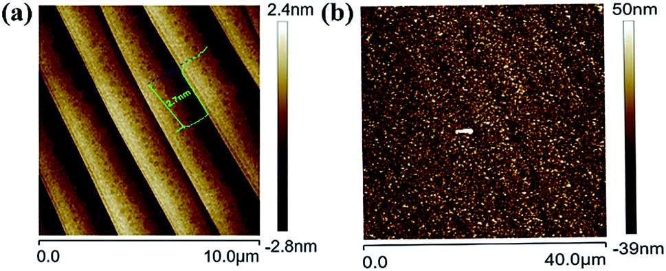 | ||
| Fig. 4 AFM topography of the SiC substrate after H-etching (a) and induced graphene growth (b). | ||
It is well known that in the Raman spectrum of graphene film, there are three major peaks around ∼1350 cm−1, ∼1580 cm−1, and ∼2700 cm−1, corresponding to the D-, G- and 2D bands, respectively.29 The G-band is an important standard to reflect the symmetry and crystal quality of graphene. The full width at half maximum (FWHM) values of the 2D-band exhibits a relationship with the number of graphene layers,30 while the D-band is the characteristic peak of non-ordered vibration of graphene and related to the concentration of defects.31
To study the chemical composition and buffer layer structure on the SiC substrate after the induced graphene growth, Raman measurements were employed. Fig. 5(a) and (b) show the Raman spectra for samples A4 and B, respectively. It is clear that the Raman intensity of sample A4 was higher than that of sample B. Furthermore, the G and 2D peaks of sample A4 were not only more independent and symmetrical than sample B but also significantly higher than those of the SiC substrate, indicating that the graphitization of sample A4 is more complete and the microscopic coverage is more uniform. The layer number of graphene grown on the SiC substrate was estimated by the full-width at haft-maximum (FWHM) of the 2D peak in Raman spectra by the following equation:30
 | (1) |
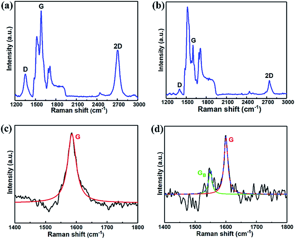 | ||
| Fig. 5 Raman spectra of sample A4 (a) and sample B (b), and the Raman spectrum around the G peak after subtracting the SiC contribution for sample A4 (c) and sample B (d), respectively. | ||
It is interesting to note that the 2D peak position of sample A4 (2700 cm−1) shows a relatively lower Raman shift compared to the sample B (2742 cm−1), and the G peak also has a relatively small shift from 1601 cm−1 (sample B) to 1584 cm−1 (sample A4). The Raman shift could reflect the variation of compressive stress between the substrate and the grown graphene. It was reported that the different thermal expansion coefficients between SiC and graphene would generate the compressive stress in the graphene layer, showing the blue shift of G and 2D peaks in the Raman spectra.34 So the red shifts of the 2D and G peaks obtained in sample A4 could be attributed to the release of the compressive stress of grown graphene. The compressive strain of graphene was estimated according to the shift of the Raman G-band with the following empirical equation:34
| ωα − ω0 = ασ | (2) |
For the purpose of elucidating the formation of nucleation sites and the induced graphene growth on SiC substrate, HRTEM measurements were performed. In order to find the graphene nucleation and growth regions, we extended the growth time of samples which underwent the same procedure as sample A4 to achieve multilayer graphene to distinguish the graphene layer and SiC layer more clearly and achieve the diffraction of graphene from the cross-section sliced by FIB. Fig. 6(a) exhibits the schematic diagram of slicing the specimen from the SiC substrate using FIB for HRTEM observation. The HRTEM specimen shown as the red box in Fig. 6(a) was lifted off the 10 mm × 10 mm SiC substrate, and the specimen was selected to contain the nucleation site and the induced grown graphene layer. Fig. 6(b) shows the SEM in situ photograph of the HRTEM specimen prepared from the substrate and transferred to the copper net for further thinning prior to the HRTEM test. Fig. 6(c) presents the typical cross-sectional HRTEM image, from which we can separate the SiC substrate, grown graphene and nucleation regions. The distance between the red dashed lines shown in Fig. 6(c) was measured to be 3.3 ± 0.2 Å, representing free-standing and single layer graphene. In addition, the distance between the first carbon layer (buffer layer) and the silicon layer at the top of the SiC substrate was measured to be 2.0 ± 0.2 Å, corresponding to the length of Si–C bonds in SiC.35,36
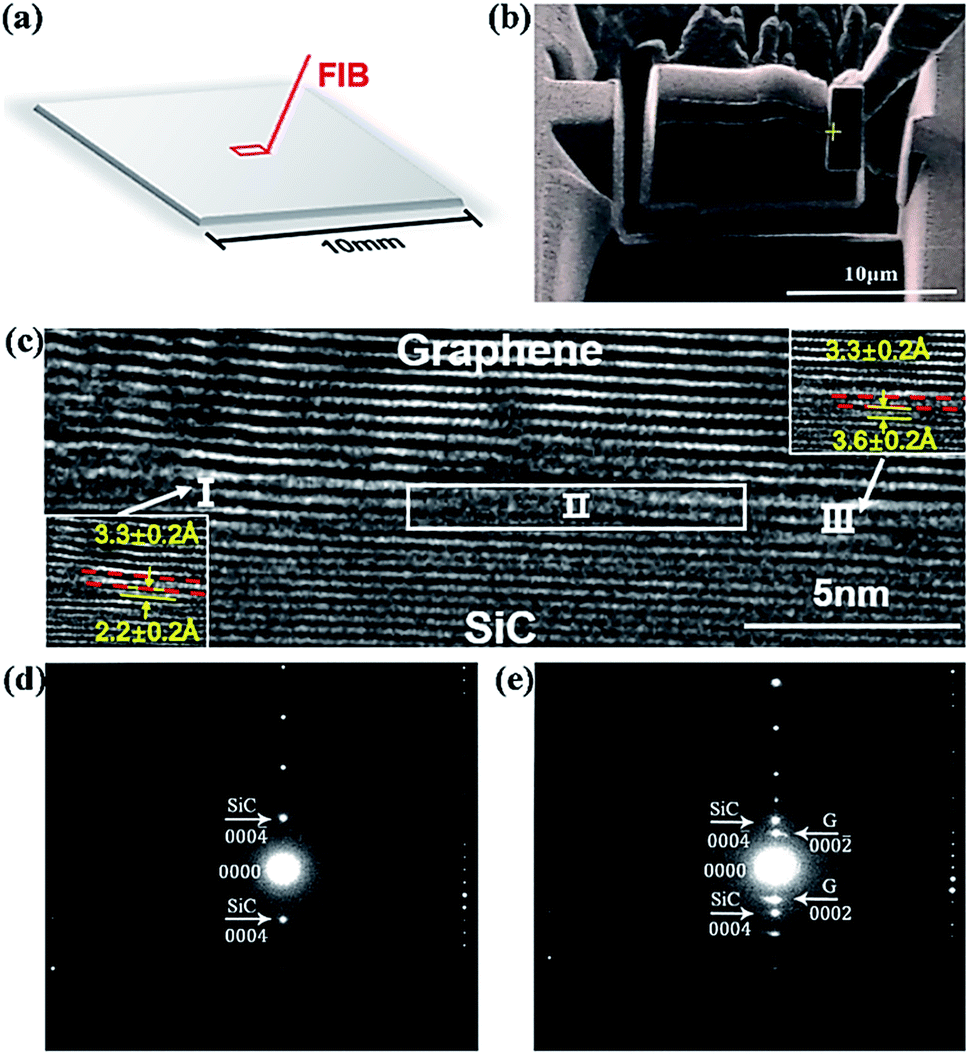 | ||
| Fig. 6 (a) Schematic diagram of slicing HRTEM specimen with FIB on a SiC substrate. (b) SEM photograph of the HRTEM specimen. (c) Cross-sectional HRTEM images of graphene layers observed on the SiC substrate. The diffraction patterns of 4H–SiC (d) and grown graphene (e) are shown. | ||
The whole HRTEM image can be divided into three parts, labeled as I, II and III, as shown in Fig. 6(c). In the Part I region with a diameter of ∼10 nm shown in the left inset, the distance between the first carbon layer and SiC was found to be 2.2 ± 0.2 Å, which is similar to that of the reported buffer layer. In combination with the growth procedure, it was presumed that this area originated from SiC decomposition and served as the nucleation site for the following graphene growth. In the part II region, the structure is slightly disordered, which is considered as the transitional area of the nucleation sites contributed from SiC decomposition and the induced grown graphene with the assistance of CH4. In the right-most Part III region, the graphene layers were found to grow along Part II. It is interesting to find that the distance of the first graphene layer on the SiC substrate was measured to be 3.6 ± 0.2 Å [the right inset in Fig. 6(c)], and the rest of the graphene layers were obtained in the distance of 3.3 ± 0.2 Å, indicating the free-standing graphene was achieved. These results are in good agreement with the XPS analysis. The diffraction patterns were collected from the 4H–SiC substrate region and the connection region between induced-grown graphene and 4H–SiC substrate. Results were presented in Fig. 6(d) and (e). Fig. 6(d) gives the diffraction pattern obtained from the SiC substrate, where the interplanar spacing was measured and found for the (0004) plane, d0004 = 2.53 Å. It was noticed that there were two sets of diffraction patterns in Fig. 6(e): one set of diffraction patterns was ascribed to the 4H–SiC (0004) plane and another set belonged to the graphene (0002) plane. The interplanar spacing of the graphene layer was measured to be d0002 = 3.57 Å, slightly higher than the theoretical interplanar distance in the graphite (d0002 = 3.35 Å (ref. 36)).
Based on the above characterizations and analysis, the mechanism of the proposed induced growth method for cultivating graphene on SiC was clarified. At first, the regular step morphology of SiC was obtained by H-etching [Fig. 1(a)]. Then the Si atoms were partially sublimated from the SiC surface when heating the sample to 1650 °C in Ar atmosphere. The remaining carbon atoms reconstructed and nucleated on the SiC substrate as shown in the red six-membered rings [Fig. 1(b)]. The inert Ar gas was used to inhibit the sublimation rate of Si atoms, thus nanoscale graphene with uniform morphology could be obtained. Afterward, low concentrations of CH4 were introduced into the chamber and decomposed as active C radicals at high temperatures. The C radicals grow preferentially centered around the nucleation sites due to the structural induction effect of the nucleation sites. Larger area graphene would be grown on the SiC substrate with continuous C radical aggregation [Fig. 1(c)]. Finally, the quasi-free-standing graphene was fabricated directly on the SiC substrate.
4. Conclusion
In this report, we presented an induced graphene growth method to prepare quasi-free-standing graphene on the Si-face of SiC substrate. The obtained quasi-free-standing graphene was further characterized and verified using XPS, Raman spectroscopy, and HRTEM measurements. The only coexistence of the graphene and SiC was revealed in the XPS spectra. Raman tests further indicated that the compressive stress of graphene grown by the induced growth method was nearly one order of magnitude lower than that prepared by the traditional epitaxial growth method on the SiC substrate. Moreover, quasi-free-standing graphene was directly observed from the typical HRTEM image, where the distance between the grown graphene and SiC substrate was 3.6 ± 0.2 Å. All these results support the significant reduction of interactions between the grown graphene and SiC substrate, showing the feasibility of this method to grow high-quality graphene for uses in the microelectronic device field.Author contributions
Zhenxing Liu, Zhen Su, and Zhiyuan Yang grew the graphene materials on SiC substrate. Qingbo Li, Li Sun and Xue Zhang characterized the graphene using the Raman and AFM. Xizheng Liu and Yingxian Li helped to do the HRTEM observations. Fapeng Yu, Yanlu Li and Xian Zhao directed this research. Zhenxing Liu, Li Sun and Fapeng Yu prepared the manuscript.Conflicts of interest
The authors declare that there are no conflicts of interest.Acknowledgements
The authors would like to thank Prof. Yi Ding at Tianjin University of Technology for the strong supports for the HRTEM experiments. This work is finally supported by the National Natural Science Foundation of China (Grand No. 51872165), the Foundation 31513020404-1 and the funding from Shandong Provincial Key Laboratory of Biophysics (SD2018BP002).References
- A. K. Geim, Science, 2009, 324, 1530–1534 CrossRef CAS.
- K. S. Novoselov, V. I. Fal, L. Colombo, P. R. Gellert, M. G. Schwab and K. Kim, Nature, 2012, 490, 192 CrossRef CAS.
- A. C. Neto, F. Guinea, N. M. Peres, K. S. Novoselov and A. K. Geim, Rev. Mod. Phys., 2009, 81, 109 CrossRef.
- K. S. Novoselov, Z. Jiang, Y. Zhang, S. V. Morozov, H. L. Stormer, U. Zeitler, J. C. Maan, G. S. Boebinger, P. Kim and A. K. Geim, Science, 2007, 315, 1379 CrossRef CAS.
- K. V. Emtsev, A. Bostwick, K. Horn, J. Jobst, G. L. Kellogg, L. Ley, J. L. McChesney, T. Ohta, S. A. Reshanov, J. Röhrl, E. Rotenberg, A. K. Schmid, D. Waldmann, H. B. Weber and T. Seyller, Nat. Mater., 2009, 8, 203 CrossRef CAS.
- Z. Yan, J. Lin, Z. Peng, Z. Sun, Y. Zhu, L. Li, C. Xiang, E. L. Samuel, C. Kittrell and J. M. Tour, ACS Nano, 2012, 6, 9110–9117 CrossRef CAS.
- A. Reina, S. Thiele, X. Jia, S. Bhaviripudi, M. S. Dresselhaus, J. A. Schaefer and J. Kong, Nano Res., 2009, 2, 509–516 CrossRef CAS.
- V. Babenko, A. T. Murdock, A. A. Koós, J. Britton, A. Crossley, P. Holdway, J. Moffat, J. Huang, J. A. Alexander-Webber and R. J. Nicholas, Nat. Commun., 2015, 6, 7536 CrossRef CAS.
- A. Burk Jr, M. O'Loughlin, R. Siergiej, A. Agarwal, S. Sriram, R. Clarke, M. MacMillan, V. Balakrishna and C. Brandt, Solid-State Electron., 1999, 43, 1459–1464 CrossRef.
- R. Yakimova, C. Virojanadara, D. Gogova, M. Syväjärvi, D. Siche, K. Larsson and L. I. Johansson, Mater. Sci. Forum, 2010, 645, 565–568 Search PubMed.
- R. Pearce, X. Tan, R. Wang, T. Patel, J. Gallop, A. Pollard, R. Yakimova and L. Hao, Surf. Topogr.: Metrol. Prop., 2014, 3, 015001 CrossRef.
- H. Nakagawa, S. Tanaka and I. Suemune, Phys. Rev. Lett., 2003, 91, 226107 CrossRef.
- W. Norimatsu and M. Kusunoki, Chem. Phys. Lett., 2009, 468, 52–56 CrossRef CAS.
- C. Riedl, C. Coletti, T. Iwasaki, A. A. Zakharov and U. Starke, Phys. Rev. Lett., 2009, 103, 246804 CrossRef CAS.
- S. Oida, F. R. Mcfeely, J. B. Hannon, R. M. Tromp, M. Copel, Z. Chen, Y. Sun, D. B. Farmer and J. Yurkas, Phys. Rev. B: Condens. Matter Mater. Phys., 2010, 82, 041411 CrossRef.
- C. Xia, S. Watcharinyanon, A. A. Zakharov, R. Yakimova and C. Virojanadara, Phys. Rev. B: Condens. Matter Mater. Phys., 2012, 85, 045418 CrossRef.
- A. L. Walter, K. J. Jeon, A. Bostwick, F. Speck and E. Rotenberg, Appl. Phys. Lett., 2011, 98, 184102 CrossRef.
- T. Hu, H. Bao, S. Liu, X. Liu, D. Ma, F. Ma and K. Xu, Carbon, 2017, 120, 219–225 CrossRef CAS.
- J. Bao, W. Norimatsu, H. Iwata, K. Matsuda and M. Kusunoki, Phys. Rev. Lett., 2016, 117, 205501 CrossRef.
- Z. Yang, S. Xu, L. Zhao, J. Zhang, Z. Wang, X. Chen, X. Cheng, F. Yu and X. Zhao, Appl. Surf. Sci., 2018, 4369, 511–518 CrossRef.
- K. V. Emtsev, A. Bostwick, K. Horn, J. Jobst, G. L. Kellogg, L. Ley, J. L. McChesney, T. Ohta, S. A. Reshanov and J. Röhrl, Nat. Mater., 2009, 8, 203–207 CrossRef CAS.
- G. G. Jernigan, B. L. VanMil, J. L. Tedesco, J. G. Tischler, E. R. Glaser, A. Davidson, P. M. Campbell and D. K. Gaskill, Nano Lett., 2009, 9, 2605–2609 CrossRef CAS.
- K. V. Emtsev, F. Speck, Th. Seyller and L. Ley, Phys. Rev. B: Condens. Matter Mater. Phys., 2008, 77, 155303 CrossRef.
- C. Yu, X. Chen, F. Zhang, L. Sun, T. Li, X. Xu and X. Zhao, J. Mater. Sci.: Mater. Electron., 2017, 28, 3884–3890 CrossRef CAS.
- P. D. Kaushik, A. Aziz, A. M. Siddiqui, G. Greczynski, M. J. Jafari, G. Lakshmi, D. Avasthi, M. Syväjärvi and G. R. Yazdi, Mater. Sci. Semicond. Process., 2018, 74, 122–128 CrossRef CAS.
- P. Aydogan, E. Arslan, S. Cakmakyapan, E. Ozbay, W. Strupinski and S. Suzer, Appl. Phys. Lett., 2015, 107, 121603 CrossRef.
- J. B. Hannon and R. M. Tromp, Phys. Rev. B: Condens. Matter Mater. Phys., 2008, 77, 241404 CrossRef.
- S. Mammadov, J. Ristein, R. J. Koch, M. Ostler, C. Raidel, M. Wanke, R. Vasiliauskas, R. Yakimova and T. Seyller, 2D Mater., 2014, 1, 035003 CrossRef.
- L. M. Malard, M. A. Pimenta, G. Dresselhaus and M. S. Dresselhaus, Phys. Rep., 2009, 473, 51–87 CrossRef CAS.
- D. S. Lee, C. Riedl, B. Krauss, K. v. Klitzing and J. H. Smet, Nano Lett., 2009, 8, 4320–4325 CrossRef.
- M. Pimenta, G. Dresselhaus, M. S. Dresselhaus, L. Cancado, A. Jorio and R. Saito, Phys. Chem. Chem. Phys., 2007, 9, 1276–1290 RSC.
- L. Sun, X. Chen, W. Yu, H. Sun, X. Zhao, X. Xu, F. Yu and Y. Liu, RSC Adv., 2016, 6, 100908–100915 RSC.
- M. Kusunoki, W. Norimatsu, J. Bao, K. Morita and U. Starke, J. Phys. Soc. Jpn., 2015, 84, 121014 CrossRef.
- Z. Ni, W. Chen, X. Fan, J. Kuo, T. Yu, A. Wee and Z. Shen, Phys. Rev. B: Condens. Matter Mater. Phys., 2008, 77, 115416 CrossRef.
- J. Borysiuk, R. Bożek, W. Strupiński, A. Wysmołek, K. Grodecki, R. Stępniewski and J. Baranowski, J. Appl. Phys., 2009, 105, 023503 CrossRef.
- J. Borysiuk, J. Sołtys, R. Bożek, J. Piechota, S. Krukowski, W. Strupiński, J. M. Baranowski and R. Stępniewski, Phys. Rev. B: Condens. Matter Mater. Phys., 2012, 85, 045426 CrossRef.
| This journal is © The Royal Society of Chemistry 2019 |