
 Open Access Article
 This Open Access Article is licensed under a Creative Commons Attribution-Non Commercial 3.0 Unported Licence
Widely applicable phosphomolybdic acid doped poly(9-vinylcarbazole) hole transport layer for perovskite light-emitting devices
Yanting
Wu
,
Zewu
Xiao
,
Lihong
He
,
Xiaoli
Yang
,
Yajun
Lian
,
Guoqing
Li
and
Xiaohui
Yang
 *
*
School of Physical Science and Technology, Southwest University, Chongqing 400715, China. E-mail: xhyang@swu.edu.cn
First published on 25th September 2019
Abstract
In this paper, a cross-linked poly(9-vinylcarbazole) (PVK):phosphomolybdic acid (PMA) layer is used as the hole transport layer in perovskite light-emitting devices, and the morphology, crystal structure, and photophysical properties of perovskite films on the PVK:PMA layer are studied. The addition of PMA into the PVK layer improves the perovskite morphology integrity and promotes hole transport. As a result, perovskite light-emitting devices using a PVK:PMA hole transport layer exhibit an improved maximum luminous efficiency of 22.1 cd A−1 and power efficiency of 18.2 lm W−1 when compared with those of the counterparts with a PVK hole transport layer. Efficient perovskite light-emitting devices can be accessed by using various antisolvents due to the good solvent resistance of PVK:PMA networks. Moreover, the luminous efficiencies of perovskite light-emitting devices with a PVK:PMA hole transport layer are almost invariant irrespective of the presence of a hole injection layer, illustrating wide applicability of the PVK:PMA hole transport layer in perovskite light-emitting devices.
Introduction
Organic–inorganic hybrid lead halide perovskites are promising for light-emitting devices due to their merits such as solution processability, band gap tunability, high luminescence efficiency, and narrow emission linewidth.1–7 Since the pioneering work on perovskite light-emitting devices by Tan et al.,1 the performance of perovskite light-emitting devices has advanced rapidly through the effort to manipulate the composition, control the morphology, and optimize the device structure.2–7 To date, the best external quantum efficiencies (EQEs) of perovskite light-emitting devices have exceeded 20%, rivalling those of organic and quantum dot light-emitting devices.8,9Poly(3,4-ethylenedioxythiophene):poly(styrenesulfonate) (PEDOT:PSS) is widely used as the hole injection/transport layer in perovskite light-emitting devices due to its relatively high work function of 4.9–5.2 eV and capability to smooth the surface of the indium tin oxide (ITO) anode.10,11 However, PEDOT:PSS, being strongly acidic and hygroscopic, interacts with the ITO electrode and perovskite layers, which adversely affects the performance and stability of related optoelectronic devices.12–15 To solve the problems of PEDOT:PSS, inorganic charge transport materials such as nickel oxide (NiOx) have been used in perovskite light-emitting devices.16–19 Chih et al.16 developed highly efficient perovskite light-emitting devices that contained a NiOx hole injection/transport layer, which showed a maximum luminous efficiency of 15.9 cd A−1. We recently propose that addition of a UV ozone-modified organic interlayer between the cuprous thiocyanate (CuSCN) hole injection layer (HIL) and perovskite layer effectively suppresses perovskite luminescence quenching by CuSCN and simultaneously allows the subsequent layering of high quality perovskite films.19
Phosphomolybdic acid (PMA) is a kegging-type compound, which comprises a phosphorous anion and twelve molybdenum oxyanions attached by three protons.20–23 Quantum dot light-emitting devices containing a PMA HIL showed reduced operating voltage and improved luminous efficiency compared with the counterpart devices with a PEDOT:PSS HIL.22 PMA was shown to induce oxidative cross-linking of PVK, and resulting robust PVK:PMA networks with high resistance against the working solvents enabled preparation of solution-processed multilayer organic light-emitting devices with excellent performances.23
Herein, we report preparation of good quality MAPbBr3 layers on the PVK:PMA layer. The addition of PMA into PVK layer promotes hole transport in light-emitting devices. MAPbBr3 light-emitting devices containing a PVK:PMA hole transport layer (HTL) show improved luminous efficiency and power efficiency when compared with the counterpart devices with a PVK HTL. Luminous efficiencies of MAPbBr3 light-emitting devices containing a PVK:PMA HTL are almost invariant irrespective of the presence of a HIL, illustrating wide applicability of PVK:PMA HTL in perovskite light-emitting devices.
Results and discussion
Characterization of PVK:PMA films
We measure UV-vis absorption spectra of PVK:PMA films with different PMA concentrations annealed at 150 °C for 5 min and those of PVK:20% PMA films annealed at different temperatures for 5 min (Fig. 1a and b). All samples exhibit a similar absorption profile with an absorption edge at ca. 350 nm, mainly originating from PVK.24 PMA shows an absorption peak at ca. 320 nm.20 The absorbance of PVK:20% PMA layers is not changed upon CB rinsing (Fig. 1c), indicating that the layers are fully cross-linked. The work function (WF) and ionization potential (IP) of the PVK layers have been determined to be 3.58 eV and 5.98 eV with ultraviolet photoelectron spectroscopy (Fig. 1d). Addition of PMA into the PVK layer increases the WF and IP to 4.17 eV and 6.37 eV, respectively, implying that PVK layer is probably p-doped by PMA deduced from a larger WF shift with respect to the IP shift,20 which facilitates hole transport.25 AFM images of the PVK and PVK:20% PMA samples annealed at 150 °C and the as-deposited PVK:20% PMA samples are shown in Fig. 1e–g, respectively. All samples show a smooth surface with the similar root-mean-square (RMS) roughness values, indicating that the addition of PMA and thermal treatment have no significant effects on the HTL morphologies. Transmission Electron Microscopy (TEM) measurements reveal that the size of PMA clusters is 25–50 nm (Fig. 1h).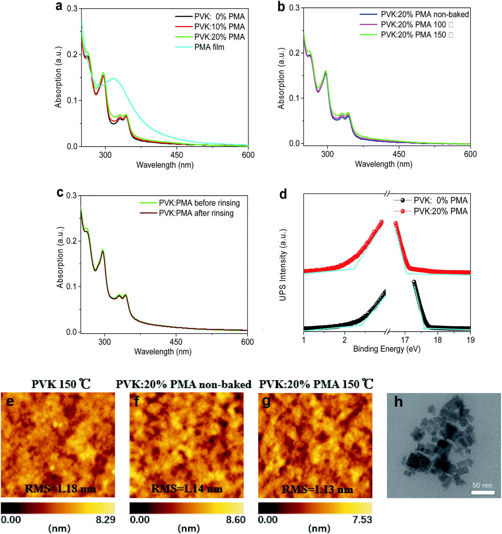 | ||
| Fig. 1 (a) UV-vis absorption spectra of PMA and PVK:PMA films with different PMA concentrations annealed at 150 °C for 5 min, (b) UV-vis absorption spectra of PVK:20% PMA films annealed at different temperatures for 5 min, (c) UV-vis absorption spectra of PVK:20% PMA films and CB-rinsed PVK:20% PMA films, and (d) secondary electron cut-off and valence band regions in UPS spectra of PVK and PVK:20% PMA films. AFM images of (e) PVK:0% PMA annealed at 150 °C, PVK:20% PMA non-annealed (f) and annealed at 150 °C (g). (h) TEM image of PVK:20% PMA film. | ||
Characterization of MAPbBr3 films
Fig. 2a and b depict X-ray diffraction (XRD) patterns of MAPbBr3 films on the ITO/CuSCN/PVK:PMA (0%, 10%, 20%), and ITO/CuSCN/PVK:20% PMA (non-baked, baked at 100 °C or 150 °C) substrates. All MAPbBr3 films show XRD diffraction peaks at 14.9°, 30.0°, and 45.8°, which are originated from the (100), (200), and (300) crystal planes of the MAPbBr3 cubic crystal structure, respectively.26 The (100) diffraction peak intensity increases upon the addition of PMA into the PVK layer and is not changed when the PMA concentration is increased from 10% to 20%, indicating that incorporation of PMA slightly increases MAPbBr3 crystallinity. Similarly, the (100) diffraction peak intensity of the sample slightly increases following thermal treatment of PVK:20% PMA layers at 100 °C and 150 °C.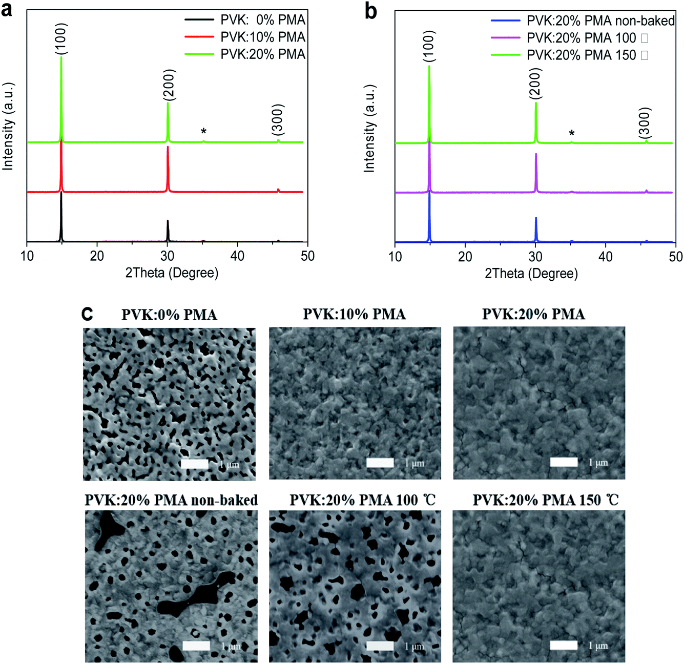 | ||
| Fig. 2 (a) XRD patterns of MAPbBr3 films on a PVK:PMA layer with different PMA concentrations, in which * represents the diffraction peak from ITO. (b) XRD patterns of MAPbBr3 films on a PVK:20% PMA layer annealed at different temperatures. (c) Top-view SEM images of MAPbBr3 films on a PVK:PMA layer with different PMA concentrations and those on a PVK:20% PMA layer annealed at different temperatures. | ||
Top-view SEM images of MAPbBr3 films on the PVK:20% PMA samples treated at different temperatures are shown in Fig. 2c. The substrate coverages of MAPbBr3 films increase with the increasing treatment temperature. MAPbBr3 films on the PVK:20% PMA layer treated at 150 °C appear fully continuous and have negligible holes or cracks. The underlying reason for this is not clear at the present stage. We hypothesize it may relate to small amount of water in PMA sample. Ohisa et al.20 reported that the water content in PMA powder increased when stored in the ambient conditions. And water was reported to induce the change of MAPbBr3 crystallinity and the formation of cracks and pin-holes.27 Top-view SEM images of MAPbBr3 films on the PVK:PMA layers with different PMA concentrations treated at 150 °C are also shown in Fig. 2c. It appears that the PMA aids to improve the MAPbBr3 morphology integrity.
The PL maxima of all MAPbBr3 samples occur at 529 nm, as shown in Fig. 3a and b. PL intensities of MAPbBr3 films decrease with increasing PMA concentration (Fig. 3a), which is possibly attributed to electron transfer from MAPbBr3 to PMA with a deep-lying WF of 6.4 eV.20 Time-resolved PL decay plots of the MAPbBr3 samples are shown in Fig. 3c. All PL decay curves can be fitted with a double exponential function, where the fast and slow components correspond to trap-mediated non-radiative recombination process and radiative electron–hole bimolecular recombination process, respectively.28 The fitting parameters are provided in Table 1. The average lifetime of MAPbBr3 films on the PVK layer (21.38 ns) is longer than those of MAPbBr3 films on the PVK:10% PMA layer (11.68 ns) and PVK:20% PMA layer (9.55 ns), which is in line with the steady-state PL measurement results.
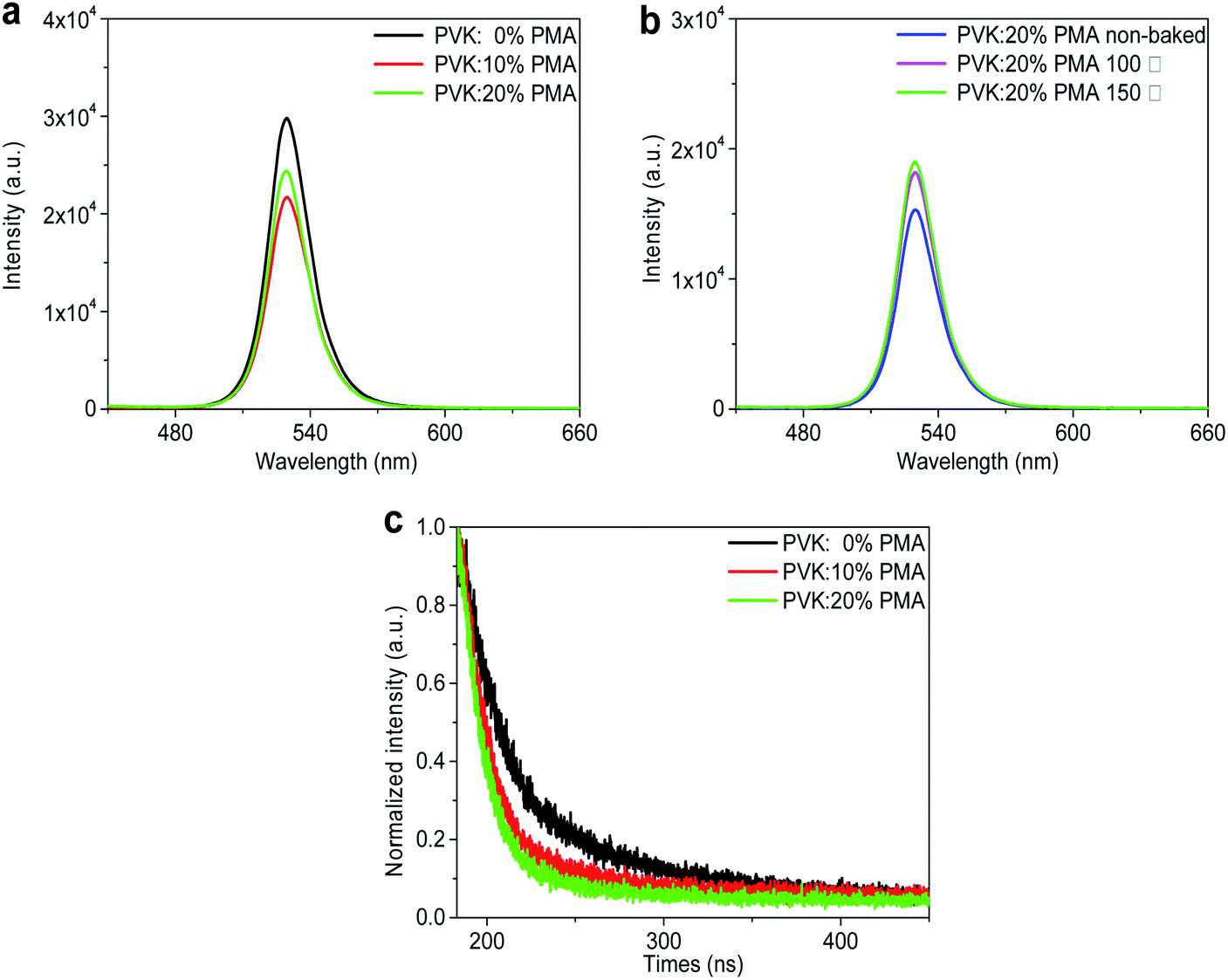 | ||
| Fig. 3 (a) PL spectra of MAPbBr3 films on the PVK:PMA layer with different PMA concentrations, (b) PL spectra of MAPbBr3 films on the PVK:20% PMA layer annealed at different temperatures. (c) Time-resolved PL decay curves of MAPbBr3 films on the PVK:PMA layer with different PMA concentrations. | ||
| τ 1 (ns) | A 1 (%) | τ 2 (ns) | A 2 (%) | τ ave (ns) | |
|---|---|---|---|---|---|
| PVK:0% PMA | 10.44 | 72 | 49.81 | 28 | 21.38 |
| PVK:10% PMA | 7.77 | 91 | 49.04 | 9 | 11.68 |
| PVK:20% PMA | 6.89 | 92 | 41.25 | 8 | 9.55 |
In addition, as the annealing temperature for PVK:20% PMA layers increases, PL intensity of the overlying MAPbBr3 layer is elevated (Fig. 3b), which may be associated with improved morphology integrity and reduced defect density in MAPbBr3 films.
Light-emitting devices
Light-emitting devices with the structure of ITO/CuSCN (15 nm)/PVK:PMA (30 nm)/MAPbBr3 (75 nm)/TmPyPB (60 nm)/CsF (1 nm)/Al (100 nm) are prepared to investigate the effects of PVK:PMA HTL incorporation on MAPbBr3 electroluminescent (EL) properties. Schematic diagrams of the devices and their energy levels are shown in Fig. 4a and b. The inset shows a cross-sectional SEM image of a MAPbBr3 layer on the PVK:20% PMA layer treated at 150 °C. A compact MAPbBr3 layer with the thickness of ca. 70–100 nm forms a good contact with the PVK:PMA layer. Except the energy levels of PVK:PMA layers (Fig. 1d), the energy levels of other materials and work function of the electrodes are obtained from the literature.3,26,29 The J–L–V and luminous efficiency–current density characteristics of the devices that contain a PVK:PMA HTL with different PMA concentrations are shown in Fig. 5a and b, respectively. Under certain voltage, current density of the devices increases with increasing PMA concentration, indicating that the addition of PMA into PVK layer promotes hole transport. Hole-dominated devices containing a PVK:20% PMA layer show larger current compared with that of the counterpart devices containing a PVK layer, confirming enhanced hole transport in the devices containing a PVK:PMA HTL (Fig. 5c). Meanwhile, the maximum luminous efficiencies of the devices increase with increasing PMA concentration, which is mainly associated with improved MAPbBr3 morphology integrity. Among the devices, the PVK:20% PMA device shows the highest maximum luminous efficiency of 22.1 cd A−1 and power efficiency of 18.2 lm W−1, respectively. | ||
| Fig. 4 (a) Schematic diagrams of the devices and (b) their energy levels. The inset shows a cross-sectional SEM image of a MAPbBr3 layer on the CuSCN/PVK:20% PMA bilayer pre-coated ITO substrate. | ||
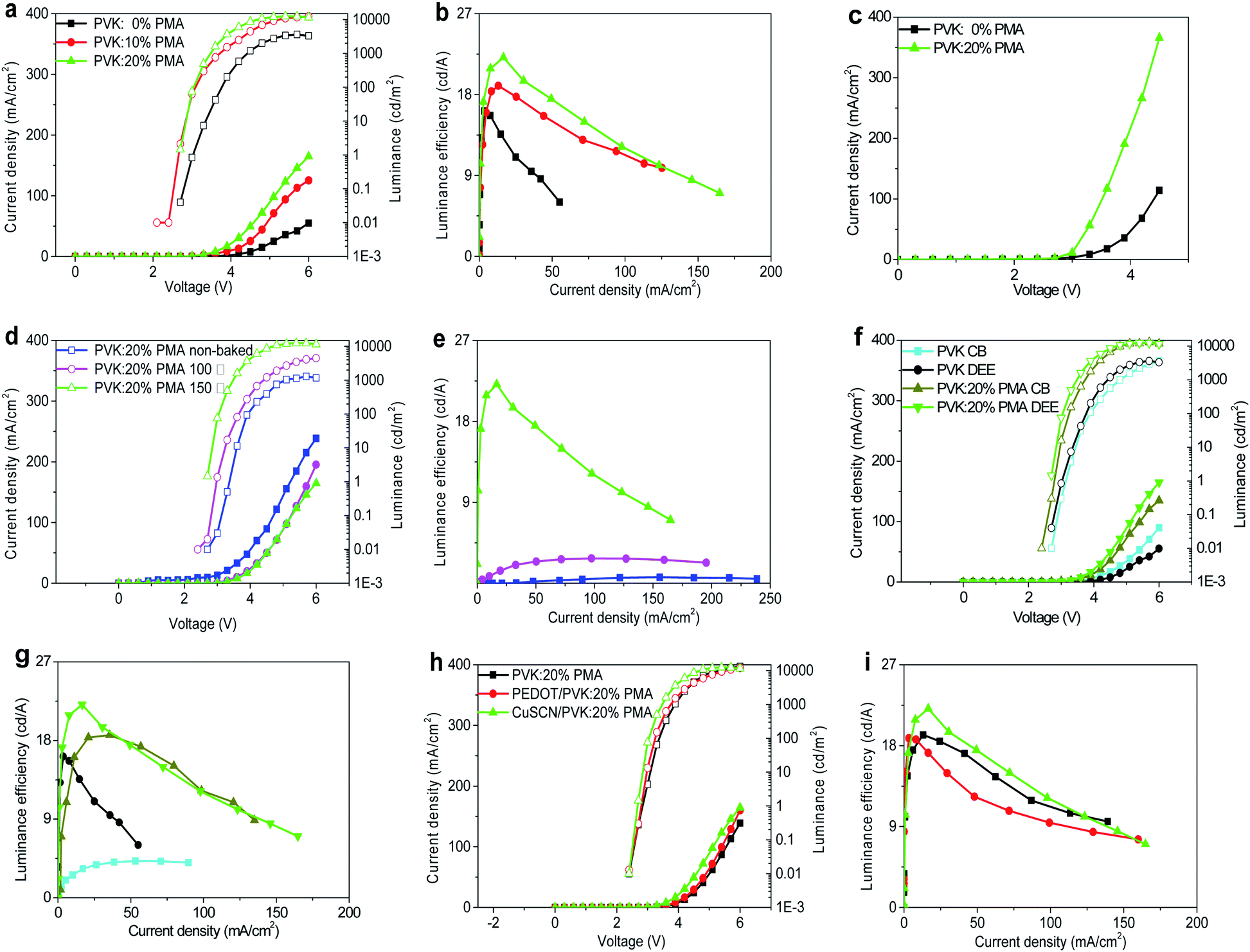 | ||
| Fig. 5 (a) J–L–V and (b) luminous efficiency–current density characteristics of light-emitting devices using a PVK:PMA HTL with different PMA concentrations. (c) J–V characteristics of the hole-dominated devices with the structure of ITO/CuSCN/PVK or PVK:20% PMA/MAPbBr3/mCP/Ag. (d) J–L–V and (e) luminous efficiency–current density properties of light-emitting devices using a PVK:20% PMA HTL annealed at different temperatures. (f) J–L–V and (g) luminous efficiency–current density plots of light-emitting devices using a PVK:20% PMA or PVK HTL processed with a CB or DEE antisolvent. (h) J–L–V and (i) luminous efficiency–current density curves of light-emitting devices with different HILs. | ||
We fix the PMA concentration to 20% and investigate how the thermal treatment temperature for PVK:PMA layers affects the performance of perovskite light-emitting devices. The J–L–V and luminous efficiency–current density characteristics of the devices are shown in Fig. 5d and e. Compared with the devices containing a PVK:20% PMA layer treated at 150 °C, the devices with an as-deposited PVK:20% PMA layer or with a PVK:20% PMA layer treated at 100 °C exhibit inferior maximum luminous efficiencies of 0.7 cd A−1 and 2.8 cd A−1, respectively, which may relate to the combinational effects of poor MAPbBr3 morphology integrity and high defect density in MAPbBr3 layers, as revealed by the SEM and steady-state PL measurements (Table 2).
| HTLs | LEmax (cd A−1) | PEmax (lm W−1) | Luminance @ 6 V (cd m−2) |
|---|---|---|---|
| PVK:0% PMA | 16.2 | 12.1 | 3324 |
| PVK:10% PMA | 19.0 | 14.8 | 12![[thin space (1/6-em)]](https://www.rsc.org/images/entities/char_2009.gif) 330 330 |
| PVK:20% PMA | 22.1 | 18.2 | 11600 |
| PVK:20% PMA non-baked | 0.7 | 0.4 | 1178 |
| PVK:20% PMA 100 °C | 2.8 | 1.7 | 4492 |
| PVK:20% PMA 150 °C | 22.1 | 18.2 | 11600 |
Due to the cross-linking nature of PVK:PMA layers, properties of light-emitting devices processed with a CB or DEE antisolvent are similar, as shown in Fig. 5f and g. By contrast, DEE-processed light-emitting devices with a PVK HTL show much higher luminous efficiencies compared with the counterpart devices processed with CB due to damaging PVK layer by CB. The results indicate use of a PVK:PMA HTL allows the wide range antisolvent selection to optimize the properties of MAPbBr3 layers without disrupting device structure.
To further illustrate wide applicability of a PVK:PMA HTL, we prepare light-emitting devices devoid of HIL, with a PEDOT:PSS or CuSCN HIL, i.e. with the structure of ITO/HIL/PVK:20% PMA (30 nm)/MAPbBr3 (75 nm)/TmPyPB (60 nm)/CsF (1 nm)/Al (100 nm) and measure the J–L–V and luminous efficiency–current density characteristics of light-emitting devices, which are shown in Fig. 5h and i. The devices with a PVK:PMA HTL show similar luminous efficiencies irrespective of the presence of a HIL, which may relate to that PVK is p-doped by PMA,25 demonstrating wide applicability of PVK:PMA layer in perovskite light-emitting devices. Note that the devices with a CuSCN or PEDOT:PSS HIL show slightly larger current compared with the devices devoid of a HIL.
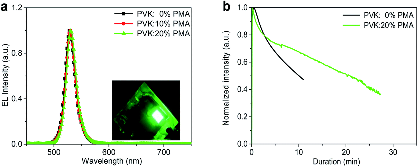
The devices containing a PVK:PMA HIL with different PMA concentrations all exhibit the characteristic MAPbBr3 emission with a maximum at 529 nm and a full width at half maximum (FWHM) value of ca. 20 nm (Fig. 6a), rendering a pure green emission with Commission Internationale de l’Eclairage (CIE) chromaticity coordinates of (0.195, 0.751). Light emission from the device with a PVK:20% PMA HIL is uniform (Fig. 6a, inset). The operational stability measurements of the devices containing a PVK or PVK:20% PMA HTL are shown in Fig. 6b. The operational lifetime (T50) of the devices containing a PVK HTL, when driven at 3 mA cm−2, is approximately 11 min. Under the same driving conditions, the devices with a PVK:20% PMA HTL exhibit a lifetime of 22 min. Improved MAPbBr3 morphology integrity on a PVK:20% PMA layer contributes to enhanced operational stability of light-emitting devices by reducing the shunt paths. Meanwhile, the addition of PMA decreases operating voltage of light-emitting devices, and as a result may reduce the effect of Joule heating on the longevity of light-emitting devices.30
 | ||
| Fig. 6 (a) EL spectra of light-emitting devices using a PVK:PMA HTL with different PMA concentrations. The inset shows a photo of a lit device with a PVK:20% PMA HTL. (b) Operational stability measurements of light-emitting devices with a PVK:20% PMA or a PVK HTL under 3 mA cm−2. | ||
Conclusion
Addition of PMA into PVK layer aids to form good quality MAPbBr3 layer and facilitates hole transport, nevertheless, slightly quenches MAPbBr3 luminescence. Perovskite light-emitting devices that contain a PVK:PMA HTL exhibit a maximum luminous efficiency of 22.1 cd A−1 and power efficiency of 18.2 lm W−1, respectively, which are superior to those of the counterpart devices containing a PVK HTL. Use of a PVK:PMA HTL allows wide range antisolvent selection due to its cross-linking nature. In addition, the devices with a PVK:PMA HTL show similar luminous efficiencies irrespective of the presence of a HIL, demonstrating wide applicability of PVK:PMA layer in perovskite light-emitting devices.Experiment section
Materials
Methylammonium bromide (MABr), lead(II) bromide (PbBr2), 1,3,5-tri(m-pyrid-3-yl-phenyl)benzene (TmPyPB), and 1,3-bis(N-carbazolyl)benzene (mCP) were purchased from Xi'an Polymer Technology (China). Poly(3,4-ethylenedioxythiophene):poly(styrenesulfonate) (PEDOT:PSS) (AI 4083) was obtained from Heraeus Corp. (Germany). CuSCN, dimethylformamide (DMF), chlorobenzene (CB), diethyl ether (DEE), and PVK were bought from Sigma-Aldrich (China). Diethyl sulfide (DES) was obtained from Shanghai Aladdin Industrial Corporation (China). Acetonitrile was purchased from Tianjin Kermel Chemical Testing Corp. (China). PMA was bought from Tokyo Chemical Industry Corp. All materials were used as received.Device fabrication
CuSCN powder was dissolved in DES with a concentration of 20 mg ml−1 at 60 °C for 1 h. PVK and mCP were dissolved in CB with respective concentrations of 6 and 8 mg ml−1. PMA was dissolved in acetonitrile with a concentration of 5 mg ml−1. MABr (63 mg, 0.53 mmol) and PbBr2 (137 mg, 0.37 mmol) were dissolved into 1 ml DMF. ITO substrates were sequentially cleaned with deionized water and organic solvents and afterward treated with UV ozone for 30 min immediately prior to device preparation. For preparation of a CuSCN HIL, the CuSCN solution was spin-coated onto the ITO substrates at 5000 rpm for 60 s. The CuSCN layers were heated at 60 °C for 3 min. For preparation of a PEDOT:PSS HIL, the PEDOT:PSS water dispersion was spin-coated on the ITO substrates, which were thermally treated at 170 °C for 10 min to remove residual water. PVK and PVK:PMA HTLs were prepared by spin-coating the solutions at 3000 rpm on the ITO substrates, PEDOT:PSS, or CuSCN layers. The PVK:PMA layers were subsequently treated at different temperatures for 5 min. The MAPbBr3 precursor solution was spin-coated at 3000 rpm. During the film formation process, 400 μl DEE or CB was dropped onto the spinning substrate to accelerate crystallization. The thickness of the MAPbBr3 layer was ca. 75 nm as determined from the cross-sectional SEM measurements. Light-emitting devices were completed by sequentially depositing TmPyPB (60 nm), CsF (1 nm), and Al (100 nm) under a vacuum of 10−4 Pa onto the MAPbBr3 layers. Hole-dominated devices were prepared by the successive deposition of mCP (15 nm) and Ag (100 nm) onto the MAPbBr3 layers. All preparation processes were conducted inside a glovebox with water and oxygen concentrations of 1 ppm except for deposition of PEDOT:PSS layers.Device characterization
The device's current density–luminance–voltage (J–L–V) characteristics were measured using a programmed Keithley 2400 source-measure unit and a Konica-Minolta chroma meter CS-100A. Electroluminescent (EL) spectra were recorded with an Ocean Optics USB4000 UV-vis spectrometer. UV-vis absorption spectra were characterized with a Shimadzu UV-2600 spectrophotometer. Steady-state PL spectra and time-resolved PL decay curves were acquired with a Hitachi F4600 fluorophotometer using an excitation wavelength of 405 nm. X-ray diffraction (XRD) patterns were measured with a Rigaku D/Max-B X-ray diffractometer equipped with a Cu Kα radiation source. Morphologies of the samples were studied using a JSF-7100 scanning electron microscope (SEM) and a Hitachi atomic force microcope (AFM). Ultraviolet photoelectron spectroscopy (UPS) measurements were performed using an ESCALAB 250Xi system. Transmission electron microscopy measurements were carried out with a FEI Talos F200 scanning/transmission electron microscope.Conflicts of interest
There are no conflicts to declare.Acknowledgements
Financial support by the National Natural Science Foundation of China (Grant No: 11474232).References
- Z. K. Tan, R. S. Moghaddam, M. L. Lai, P. Docampo, R. Higler, F. Deschler, M. Price, A. Sadhanala, L. M. Pazos, D. Credgington, F. Hanusch, T. Bein, H. J. Snaith and R. H. Friend, Nat. Nanotechnol., 2014, 9, 687–692 CrossRef CAS.
- H. Cho, S. H. Jeong, M. H. Park, Y. H. Kim and T. W. Lee, Science, 2015, 350, 1222–1225 CrossRef CAS.
- S. A. Veldhuis, P. P. Boix, N. Yantara, M. J. Li, T. C. Sum, N. Mathews and S. G. Mhaisalkar, Adv. Mater., 2016, 28, 6804–6834 CrossRef CAS.
- L. N. Quan, F. P. G. de Arquer, R. P. Sabatini and E. H. Sargent, Adv. Mater., 2018, 30, 1801996 CrossRef.
- S. D. Stranks and H. J. Snaith, Nat. Nanotechnol., 2015, 10, 391–402 CrossRef CAS.
- N. N. Wang, L. Cheng, R. Ge, S. T. Zhang, Y. F. Miao, W. Zou, C. Yi, Y. Sun, Y. Cao, R. Yang, Y. Q. Wei, Q. Guo, Y. Ke, M. T. Yu, Y. Z. Jin, Y. Liu, Q. Q. Ding, G. C. Xing, H. Tian, C. H. Jin, F. Gao, R. H. Friend, J. P. Wang and W. Huang, Nat. Photonics, 2016, 10, 699–704 CrossRef CAS.
- B. R. Sutherland and E. H. Sargent, Nat. Photonics, 2016, 10, 295–302 CrossRef CAS.
- Y. Cao, N. Wang, H. Tian, J. Guo, Y. Wei, H. Chen, Y. Miao, W. Zou, K. Pan, Y. He, H. Cao, Y. Ke, M. Xu, Y. Wang, M. Yang, K. Du, Z. Fu, D. Kong, D. Dai, Y. Jin, G. Li, H. Li, Q. Peng, J. Wang and W. Huang, Nature, 2018, 562, 249–253 CrossRef CAS.
- K. Lin, J. Xing, L. N. Quan, F. P. G. de Arquer, X. Gong, J. Lu, L. Xie, W. Zhao, D. Zhang, C. Yan, W. Li, X. Liu, Y. Lu, J. Kirman, E. H. Sargent, Q. Xiong and Z. Wei, Nature, 2018, 562, 245–248 CrossRef CAS.
- S. Ahn, S. H. Jeong, T. H. Han and T. W. Lee, Adv. Opt. Mater., 2017, 5, 1600512 CrossRef.
- Y. W. Zhu, Z. C. Yuan, W. Cui, Z. W. Wu, Q. J. Sun, S. D. Wang, Z. H. Kang and B. Q. Sun, J. Mater. Chem. A, 2014, 2, 1436–1442 RSC.
- M. Jorgensen, K. Norrman and F. C. Krebs, Sol. Energy Mater. Sol. Cells, 2008, 92, 686–714 CrossRef.
- H. Luo, X. Lin, X. Hou, L. Pan, S. Huang and X. Chen, Nano-Micro Lett., 2017, 9, 39 CrossRef.
- G. A. D. Benatto, B. Roth, M. V. Madsen, M. Hosel, R. R. Sondergaard, M. Jorgensen and F. C. Krebs, Adv. Energy Mater., 2014, 4, 1400732 CrossRef.
- D. W. Zhao, M. Sexton, H. Y. Park, G. Baure, J. C. Nino and F. So, Adv. Energy Mater., 2015, 5, 1401855 CrossRef.
- Y. K. Chih, J. C. Wang, R. T. Yang, C. C. Liu, Y. C. Chang, Y. S. Fu, W. C. Lai, P. Chen, T. C. Wen, Y. C. Huang, C. S. Tsao and T. F. Guo, Adv. Mater., 2016, 28, 8687–8694 CrossRef CAS PubMed.
- Z. B. Wang, Z. Luo, C. Y. Zhao, Q. Guo, Y. P. Wang, F. Z. Wang, X. M. Bian, A. Alsaedi, T. Hayat and Z. A. Tan, J. Phys. Chem. C, 2017, 121, 28132–28138 CrossRef CAS.
- L. Liu, Z. B. Wang, W. D. Sun, J. Zhang, S. Q. Hu, T. Hayat, A. Alsaedi, T. Hayat and Z. A. Tan, Chem. Commun., 2018, 54, 13283–13286 RSC.
- Y. T. Wu, Z. W. Xiao, Y. J. Lian, X. F. Peng, L. L. He, X. L. Yang, Q. Wang, J. Ren, G. Q. Li and X. H. Yang, Org. Electron., 2019, 75, 105420 CrossRef CAS.
- S. Ohisa, S. Kagami, Y. J. Pu, T. Chiba and J. Kido, ACS Appl. Mater. Interfaces, 2016, 8, 20946–20954 CrossRef CAS.
- M. Chrzanowski, M. Banski, P. Sitarek, J. Misiewicz and A. Podhorodecki, RSC Adv., 2019, 9, 10754–10759 RSC.
- D. Dong, L. Lian, H. Wang and G. F. He, Org. Electron., 2018, 62, 320–326 CrossRef CAS.
- N. Aizawa, Y. J. Pu, T. Chiba, S. Kawata, H. Sasabe and J. Kido, Adv. Mater., 2014, 26, 7543–7546 CrossRef CAS.
- C. Zhang, H. Von Seggern, K. Pakbaz, B. Kraabel, H. W. Schmidt and A. J. Heeger, Synth. Met., 1994, 62, 35–40 CrossRef CAS.
- G. F. He, K. Leo, M. Hofmann, J. Birnstock, R. Pudzich and J. Salbeck, Appl. Phys. Lett., 2004, 85, 3911–3913 CrossRef CAS.
- X. F. Peng, X. Y. Wu, X. X. Ji, J. Ren, Q. Wang, G. Q. Li and X. H. Yang, J. Phys. Chem. Lett., 2017, 8, 4691–4697 CrossRef CAS.
- H. R. Wang, X. M. Li, M. J. Yuan and X. Y. Yang, Small, 2018, 14, 1703410 CrossRef.
- J. Z. Chen and N. G. Park, Adv. Mater., 2018, 30, 1803019 CrossRef.
- Q. Xiong, H. Tian, J. Zhang, L. Han, C. Y. Lu, B. H. Shen, Y. Zhang, Y. J. Zheng, C. J. Lu, Z. B. Zeng, Z. Y. Hu, L. H. Wu and Y. J. Zhu, Org. Electron., 2018, 61, 151 CrossRef CAS.
- Z. G. Xiao, R. A. Kerner, L. F. Zhao, N. L. Tran, K. M. Lee, T. W. Koh, G. D. Scholes and B. P. Rand, Nat. Photonics, 2017, 11, 108–115 CrossRef CAS.
| This journal is © The Royal Society of Chemistry 2019 |