
 Open Access Article
 This Open Access Article is licensed under a Creative Commons Attribution-Non Commercial 3.0 Unported Licence
Reaction induced morphology changes of tetracene and pentacene surfaces†
Feifei Li and
Jacob W. Ciszek*
and
Jacob W. Ciszek*
Department of Chemistry and Biochemistry, Loyola University Chicago, 1032 West Sheridan Road, Chicago, Illinois 60660, USA. E-mail: jciszek@luc.edu
First published on 28th August 2019
Abstract
Morphology plays a critical role in determining the properties of solid-state molecular materials, yet fluctuates wildly as these materials undergo reaction. A prototypical system, a vapor–solid Diels–Alder reaction of tetracene and pentacene thin-films, is used to observe the evolution of morphology features as the reaction transitions from surface to bulk. The initial stages of reaction display little topographical change as measured by atomic force microscopy (AFM) and scanning electron microscopy (SEM), and substrates are coated with a uniform layer of product 1–2 molecules thick, as determined by energy-dispersive X-ray (EDX) spectroscopy. The highly textured surfaces of late stage reactions are a result of aggregated products, as identified via EDX spectroscopy and polarization modulation infrared reflection absorption spectroscopy (PM-IRRAS); areas of the surface in between product aggregates resemble the initial stages. The mechanism by which products aggregate into surface asperities requires the assistance of a facilitating media – in this case condensed vapor; simple thermally assisted surface diffusion was unable to generate these morphology changes. The combined data indicate that reactions of molecular solids, could be confined to the surface in the absence of condensate of the vapor phase reactant.
Introduction
In molecular solids, morphology effects often exceed the influence of chemical functionalities in determining the materials properties. For example, in organic light emitting diodes, pyridyl tetrazolate complexes display tunable color and efficiency based on thin film morphology which dictates the concentration of dimer states.1 In organic transistors, the degree of crystallinity and orientation of the molecules within the film dominate transport properties such as mobility.2,3 In pharmacology, Ritonavir is a classic example of drug efficacy impacted by morphology; here Form II's decreased solubility and its incompatibility with formulation resulted in a market crisis for its manufacturer.4 Numerous other examples fill the literature.5–7Due to this outsized role in materials properties, it is important to understand reactions of these molecular materials from a morphological standpoint as well as a chemical one.8 Morphological changes are quite common in reactions of molecular solids. Excepting single crystal to single crystal reactions,9 the reaction of molecular solids generally produces compounds that are unable to fit within the original lattice structure. The geometrical mismatch with the original lattice generates pressure which can be relieved by lattice rearrangement or, more commonly, molecular migration.10 The result is a solid whose morphology bears little resemblance to the original structure. These changes have been extensively reported for molecular substrates such a crystalline p-carboxyaniline, anthracenes, and benzimidazole.11
While the final systems are well characterized, the mechanism by which these interfacial reactions proceed is still poorly defined. Kaupp has extensively classified the formed topography of the reacted molecular surfaces (craters, islands, floes, etc.)12 but the findings lack any relationship between chemical structure and formed topographies. Braga has performed extensive studies on the final polymorphic forms of barbituric acid or ferrocene dicarboxylic acid reacted with amines,13,14 but information on reaction propagation is absent. These works have a limited ability to establish reaction mechanisms because they miss the transient states associated with the initial surface reaction. For example, little is known about reactant adsorption phenomena which should dictate the kinetics of the reaction and morphology changes. Basic information such as the surface coverage during reaction (which could determine whether formed products passivate the surface and inhibit further reaction) is lacking.15 Even the composition of various morphology features observed in incomplete reactions is unknown.16 In concert, this information could shine light on the mechanism by which surface reactions propagate into the subsurface and bulk.16,17 It is essential to answer these questions as surface phenomenon generally dominate the processes for the reaction of solid materials.18–21
This can be studied via Diels–Alder reaction of vapor-phase adsorbates with pentacene and tetracene thin film. These particular materials have extensive film characterization22–29 and are prototypical organic semiconductors. Pentacene, in particular, is a ubiquitous transistor material,30–33 and has functioned as hole injection layer in OLEDs,34 the semiconductor in metal-insulator-semiconductor (MIS) memory,35 or even as a sensitizers in singlet-fission solar cells.36 The acenes also contain numerous double bonds which are primed to react with a dienophile via a Diels–Alder reaction, whereby a vapor-phase adsorbate bonds to the surface. The Diels–Alder reaction itself is a simple, concerted, bi-molecular reaction which generates no biproducts.37 As such, monitoring the surface species generated within this study is simplified. Its 90 years of history provide ample groundwork on the rates, transition states, isomer stabilities, stereostructures, and stability,37 all of which may impact solid state reactivity. This precedence includes a handful of studies on the reaction of these molecular surfaces, precedence which guides the experiments herein.15–17
Within this work, we report on transient states formed during Diels–Alder reaction of tetracene and pentacene molecular surfaces. Surface topography is continuously monitored to observe surface passivation and later surface asperity formation (Fig. 1), while correlating these observations with changes in molecular identity. A model describing morphology evolution can be formed when this data is coupled with similar measurements tracking the composition of the underlying substrate. This, and the subsequent mechanistic insight, has great importance for generating monolayer type materials for interface engineering15,38,39 as well as complete reaction of molecular materials.
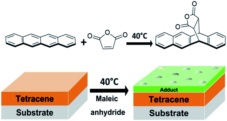 | ||
| Fig. 1 General mechanism for the Diels–Alder reaction between tetracene thin film and vapor-phase maleic anhydride. | ||
Experimental section
Materials
All evaporation metals are of 99.9% or greater purity. Sublimed grade tetracene and pentacene, maleic anhydride, N-methylsuccinimide, and 200 proof ethanol (ACS grade) were commercially obtained and used without further purification. The standard N-methylmaleimide-tetracene adduct was synthesized as reported previously.40Preparation of gold substrates
Cut microscope slides (11 × 25 × 1 mm) were cleaned in piranha solution (3![[thin space (1/6-em)]](https://www.rsc.org/images/entities/char_2009.gif) :1, H2SO4:H2O2) for 30 min. The slides were rinsed with copious amounts of 18 MΩ water and 200 proof ethanol, sonicated for 20 min in ethanol, and dried under a stream of nitrogen. Microscope slides were then mounted in a thermal evaporator (Kurt J. Lesker NANO38). A 5 nm chromium adhesion layer was deposited, followed by 100 nm of gold at a base pressure of <1 × 10⁻⁶ torr. Both metals were evaporated at a rate of 1 Å s−1.
:1, H2SO4:H2O2) for 30 min. The slides were rinsed with copious amounts of 18 MΩ water and 200 proof ethanol, sonicated for 20 min in ethanol, and dried under a stream of nitrogen. Microscope slides were then mounted in a thermal evaporator (Kurt J. Lesker NANO38). A 5 nm chromium adhesion layer was deposited, followed by 100 nm of gold at a base pressure of <1 × 10⁻⁶ torr. Both metals were evaporated at a rate of 1 Å s−1.
Deposition of tetracene thin film
Tetracene was placed onto a cartridge heater at the bottom of a home built sublimation chamber. A freshly prepared gold substrate was added to the chamber. Upon evacuation to a base pressure 3 × 10⁻⁶ torr, liquid nitrogen was added to the trap system and the heater was turned on. Thickness was monitored via quartz crystal microbalance (QCM) and when a stable deposition rate of 1 Å s−1 was reached, the substrate shifted into the main chamber for deposition. Deposition continued until the film reached a thickness of 100 nm and then the sample was removed. After deposition, the substrate was allowed to cool under high vacuum for 30 min.Deposition of pentacene thin film
The 50 nm pentacene thin films were deposited using the same protocol as the above tetracene thin films deposition process, but at slightly higher source temperatures.Diels–Alder reactions on thin-film surfaces
Tetracene/pentacene thin-film substrates were placed into a 100 mL Schlenk tube sealed with a hollow end stopper along with approximately 8 mg of solid adsorbate in a small vial. The air within the Schlenk tube was evacuated and filled with nitrogen three times. The sealed vessel was then heated in a furnace at the temperatures described in the main text. After completion of the reaction (8–72 h), the vapor-phase dienophiles were condensed away from the substrate by cooling one end of the flask with dry ice. Any physisorbed material was removed by first exposing the sample to less than 10−2 torr (roughing pump) for 15 min before subjecting it to pressures less than 10−5 torr (turbomolecular pump) for 1 h.Deposition of standard N-methylmaleimide-tetracene adduct
The solution synthesized standard N-methylmaleimide-tetracene adduct40 was placed into a cartridge heater at the bottom of a home built sublimation chamber. A freshly prepared 100 nm tetracene substrate was added to the chamber. Upon evacuation to a base pressure 3 × 10⁻⁶ torr, liquid nitrogen was added to the trap system and the heater was turned on. Thickness was monitored via QCM and when a stable deposition rate of 1 Å s−1 was reached, the substrate shifted into the main chamber for deposition. Deposition continued until the film reached a thickness of 7 nm and then the sample was removed. After deposition, the substrate was allowed to cool under high vacuum for 30 min.PM-IRRAS analysis of thin films
The composition of the thin films was assessed both before and after the reaction via polarization modulation infrared reflection absorption spectroscopy using a Bruker Optics Tensor 37 FTIR equipped with a PMA 50 accessory and a MCT detector. The reaction progress was assessed by comparing newly generated IR vibrations to those within a spectrum of a standard solution-synthesized adduct, and additional information gleaned from the consumption of substrate peaks. The thin films were analyzed at a resolution of 8 cm−1.Atomic force microscopy imaging of thin films
The surface morphologies of the 100 nm continuous tetracene thin film and tetracene thin films that had been reacted for 8 h with maleic anhydride were analyzed using atomic force microscopy. The thin films were imaged in air with NTEGRA SPM (NT-MDT Spectrum Instruments, Moscow, Russia). The instrument was operated in Amplitude Modulation (tapping) mode using Si AFM cantilevers (NSG10, NT-MDT Spectrum Instruments) with a nominal tip radius of 6 nm. The images were collected at scan rate of 1 Hz and are 512 × 512 points. The root-mean-square (rms) roughness of the thin films (both pure tetracene and 8 h maleic anhydride tetracene adduct) was calculated from the obtained topography images using Image Analyses software (NTEGRA SPM (NT-MDT Spectrum Instruments)).Scanning electron microscope imaging and energy dispersive X-ray spectrometer analysis on thin films
Thin-film surface topography and morphology were studied using a HITACHI SU3500 scanning electron microscope equipped with a QUANTAX Compact system for energy dispersive X-ray spectroscopy. The QUANTAX Compact system contains a 30 mm2 silicon drift detector capable of 129 eV energy resolution. The accelerating voltage was between 1–5 keV. The spectrometer signal intensity was roughly 10k cps. SEM images were acquired at an accelerating voltage between 1–5 keV and a sample angle of either 0° or 85°.Results and discussion
The morphologies for tetracene and pentacene films are well established. When deposited onto most surfaces, the molecules adopt a thin-film phase, whereby the molecules are oriented perpendicular to the surface in a compressed unit cell.22 This can be interconverted to the bulk phase, where the acenes are slightly tilted from the surface normal via exposure to solvent or other means.22 It is also possible to orient tetracene and pentacene planar on the surface: the initial molecules prefer a flat orientation when deposited onto a clean, high-energy surface.23,24 Additional deposited material maintains this planar orientation.25 Grazing angle X-ray diffraction commonly distinguishes between the two perpendicular phases ((001 and 001′) orientation) and the planar orientation (mostly (110)).22,25,26 Additionally, infrared spectroscopy can be an effective tool for providing this same information. The out-of-plane bending vibrations of the aromatic rings (907, 731 cm−1) dominate the planar orientation while numerous ring stretches (1445, 1162, 990 cm−1) appear prominently in the thin-film and bulk phase. Within the perpendicular orientations, crystalline domains are readily expressed; grains range from 0.8 μm to 5 μm and can be controlled via deposition temperature.27 In contrast, planar orientation of the molecules forms smaller rod-like domains. More extensive details can be found in recent reviews.28,29 This work focuses primarily on the planar oriented acenes, and representative infrared (IR), atomic force microscopy (AFM), and scanning electron microscopy (SEM) data can be found in Fig. 2.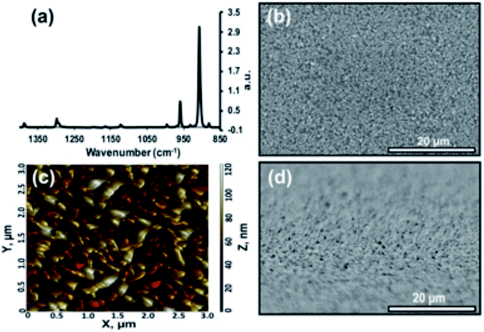 | ||
| Fig. 2 Continuous tetracene thin film (100 nm) with molecules in planar orientation. (a) PM-IRRAS spectrum showing the out-of-plane bend at 907 cm−1. (b) SEM image at an electron energy of 5 keV. (c) AFM image measured in tapping mode. The RMS roughness of this area is 20 nm. (d) SEM image with sample tilted 85° at an electron energy of 5 keV. | ||
This work began by reacting the planar-oriented tetracene in Fig. 2 with vapors of maleic anhydride at 40 °C. Over the span of 45 h, the reaction was intermittently examined via IR which provides the ability to observe both substrate and product signals. As seen in Fig. 3a and b, the reaction proceeds in a fairly linear fashion with the increase in product occurring nearly in lock step with reaction time. The product carbonyl stretch (ca. 1770 cm−1) and ring deformation (ca. 940 cm−1)41 indicated in the figure correspond only to covalently bonded species as unreacted maleic anhydride is eliminated during the reaction workup.15 The signal intensity at 8 h roughly corresponds to a 1–2 molecule thick layer of coverage,17 with later points being proportionally more. Complementary changes were also seen in signals from the underlying substrate. IR measurements indicate that roughly 2% of the tetracene film is consumed at the first point (8 h), while 17% of the tetracene remains at the reactions termination (45 h) (Fig. S1, ESI†).
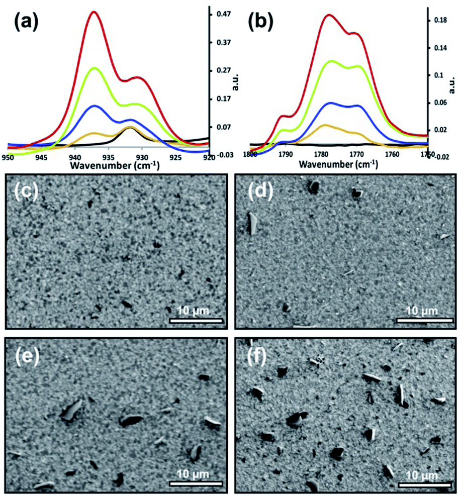 | ||
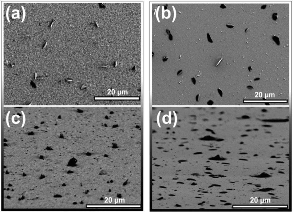
| Fig. 3 (a, b) PM-IRRAS spectra of the reaction between a 100 nm tetracene thin film and maleic anhydride at different reaction times. From top to bottom: red (45 h), green (36 h), blue (18 h), orange (8 h), and black (pure tetracene). (c–f) SEM images of corresponding maleic anhydride reacted tetracene thin-films at different reaction times: (c) 8 h, (d) 18 h, (e) 36 h, (f) 45 h. All SEM images were taken at an electron energy of 5 keV. | ||
These initial stages of thin-film reaction progress were then examined for morphology changes via SEM. As can be seen in Fig. 3c–f, the reaction progress had a non-linear effect on the surface morphology. After 8 h, the surface appears to be mostly unperturbed, with only a handful of nanometer size features observable, and surface morphology appears unchanged at this point. This is interpreted to mean the majority of the 1–2 molecular layers of reaction product is distributed somewhat evenly over the surface (confirmed later via topographic and spectroscopic measurements, vide infra). The 8 h data is in stark contrast to subsequent time points, where dark asperities begin to form on the surface. These dark features reached nearly 5 μm in size and the areas they occupy increased with time. Beyond the first 8 hours, any additional product formed (IR) is strongly correlated with the sizes of the asperities. Because of this relationship, the asperities are presumed to be product.
The asperities' identity was confirmed to be product based off SEM and energy-dispersive X-ray (EDX) spectroscopy of extended reactions (Fig. S2, ESI†). Surfaces reacted for 7 and 10 days were shown to have 68% and >90% of the tetracene consumed (IR), and asperities continued to grow until all the substrate is consumed (Fig. 4a). EDX analysis of highly reacted surfaces show the dark asperities to be comprised nearly entirely of carbon and oxygen in roughly a 1:10 ratio consistent with the molecular formula of the adduct (C22H14O3). EDX data has been mapped (Fig. 4) and the associated elemental analysis can be found in the ESI (Fig. S3, ESI†). Since these product asperities are not observed in the initial 8 h images, we postulate that, at this early time, a 1–2 molecule thick layer initially forms, and any additionally generated product begins to aggregate if the reaction is allowed to continue.
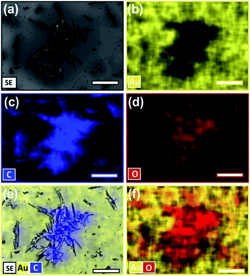 | ||
| Fig. 4 SEM imaging and EDX element distribution mapping of aggregated features on a tetracene surface that has been fully reacted with maleic anhydride (72 h, 50 °C). Data taken at 5 keV. (a) SEM imaging. (b) Au distribution map. (c) C distribution map. (d) O distribution map (e) merged SEM image, with Au and C distribution maps. (f) Merged Au and O distribution maps. Scale bars are 60 μm. | ||
The aggregates of product appear general to reactions of molecular surfaces, but their appearance can be quite varied. Similarly shaped asperities have been reported before with the combination of N-methylmaleimide with pentacene16 and tetracene.15 Additionally, we have found pentacene films reacted with maleic anhydride (50 °C, 2.5 h) also form these same aggregates of product (Fig. 5). Both our data and previous reports are consistent with a mechanism where the initial reaction has minimal aggregation, but a later step results in the formation of product clusters. It is also important to note that not all aggregates are identical in morphology. The dark aggregates of product found when reacting tetracene with maleic anhydride protrude from the surface. This can be seen in Fig. 5c where the sample has been tilted 85°. Here, all of the largest features are observed to protrude from the surface; the largest 20 features extended out roughly 1 μm. Product aggregates on pentacene (Fig. 5d) were markedly different. Here only the very largest of the aggregates had any measurable height, most appear to wet the surface. Additionally, aggregates differ in texture; protrusions on tetracene display rough edges, while on pentacene the product aggregates are smooth and almost molten. It is important to note that this difference is not just a function of reaction temperature – tetracene samples reacted at 50 °C (e.g. Fig. S4, ESI†) also protrude from the surface after 2.5 h and during extended reaction evolve to a crystalline like appearance, similar to Fig. 4a.
 | ||
| Fig. 5 (a) SEM image of a 100 nm thick tetracene thin film reacted for 18 h at 40 °C with maleic anhydride. (b) SEM image of a 50 nm thick pentacene thin film reacted for 2.5 h at 50 °C with maleic anhydride adduct. (c) SEM image of the same tetracene thin film as in (a) tilted 85°. (d) SEM image of the same pentacene thin film as in (b) tilted 85°. All SEM images were taken at an electron energy of 5 keV. | ||
A series of three measurements were then performed to confirm our basic model of surface composition. First, the 8 h sample was reexamined via EDX to confirm the extent of coverage at the initial stage of reaction. As mentioned earlier, the intensity of the carbonyl stretches corresponds to a reaction that has converted the top 1–2 molecular layers (∼2–4 nm) while the lack of visible aggregates suggest that the product is dispersed over the surface. EDX analysis confirmed this. At a low acceleration voltage (1 keV) the percentage of oxygen over this surface is 2.1% (Fig. 6a and S5, ESI†). This is in good agreement with Monte Carlo simulations of a model containing 2 nm of product (C22H14O3), on top of 98 nm of tetracene (C18H12), here the simulated spectrum contains 2% oxygen (Fig. S6, ESI†).42 Moreover, elemental maps show an even distribution of the product's oxygen across the surface (Fig. 6b). Even below a 50 μm sampling dimension, the oxygen levels (and coverage of product) remains uniform over the surface.
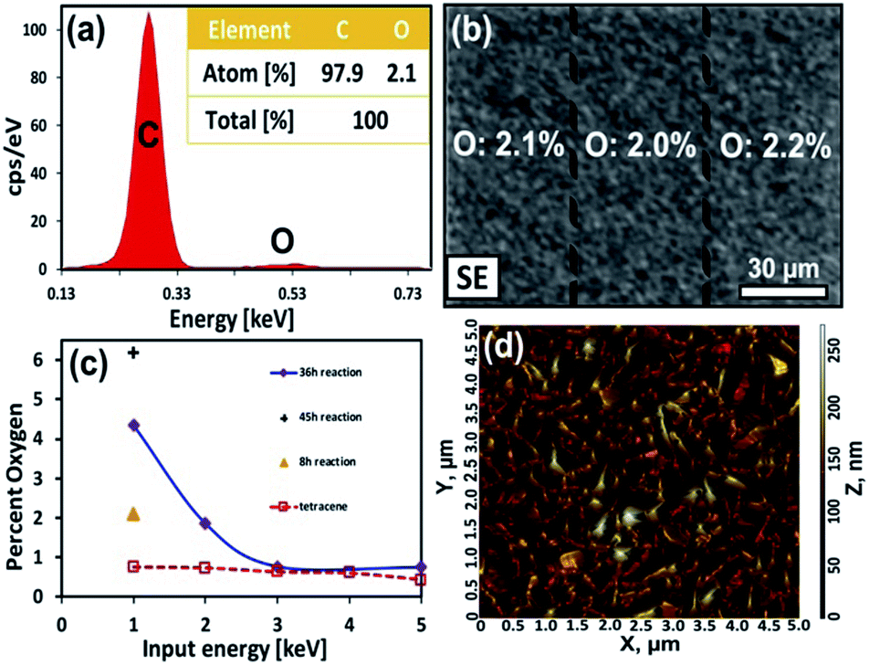 | ||
| Fig. 6 (a) EDX spectrum of a 100 nm thick tetracene thin film reacted for 8 h at 40 °C with maleic anhydride. The insert provides quantification of the atomic composition. (b) SEM image of a 100 nm thick tetracene thin film reacted for 8 h at 40 °C with maleic anhydride. The percentage oxygen for each region was determined by EDX. (c) Percentage oxygen in the film as a function of increasing acceleration voltage (providing greater depth analysis). (d) AFM image of a 100 nm thick tetracene thin film reacted for 8 h at 40 °C with maleic anhydride. The RMS roughness of this area is 32 nm. | ||
For the second measurement, it is important to confirm the integrity of the underlying tetracene substrate and show that products do not diffuse appreciably throughout the film. EDX measurements were performed with successively higher electron energies (2, 3 and 5 keV), which extends the interaction volume of the electron beam deeper into the film. For example, at 5 keV a notable amount of the underlying gold surface can be detected. In these measurements, the carbon content increases significantly with deeper electron penetration and the oxygen levels drop appreciably (Fig. 6c and S7, ESI†). As such, we conclude pristine tetracene is the predominant species underneath the reacted surface.
Third, the evolution of surface morphology during the initial stages of the reaction can provide a hint as to the mechanism of aggregate formation. Here, the fine topographical features of the 8 h sample were examined via AFM. The data shows that surface texture has changed only slightly at the initial stage of reaction. The reacted surface has a RMS roughness of 32 nm (Fig. 6d) and is now slightly rougher than the original tetracene surface which had an RMS roughness of 20 nm (Fig. 2d). Overall, this change in roughness is to be expected as the “Y”-shaped product has a substantial lattice mismatch with the linear molecules of tetracene. But the results also seem to suggest that little aggregation has occurred at this initial stage of reaction.
With these results, we can begin to formulate mechanisms for aggregate formation. Three possibilities are proposed. In the first, morphology changes are driven exclusively by lattice mismatches between the reactant and product and pressure is relieved via the formation of new asperities.10 A second explanation is that these changes occur via highly mobile surface species which self aggregate.16 In fact, surface diffusion of materials requires little thermal activation and can readily occur at cryogenic temperatures.43 Since the molecular geometry of the reactant and product are quite orthogonal and their functionalities ill-suited for co-crystallization, self-aggregation is quite favorable. The final possibility is that aggregation is not solely a thermal event, but rather, induced by a small amount of condensate of the maleic anhydride. This mechanism is supported by reports of vapor acceleration in solid phase reactions.44,45
The latter mechanism was differentiated from the former two by using a deposited film of product, rather than forming the adduct, in situ, via reaction. Here, a 7 nm thick film of the standard N-methylmaleimide-tetracene adduct was directly deposited on the surface of 100 nm of tetracene. For the first step of this experiment, the surface was heated at 40 °C for 24 h. As apparent by comparing the original film (Fig. 7a) to the annealed film (Fig. 7b), no aggregates are seen. Spectroscopically, the results are similar. No appreciable reorientation is seen in either the product or the underlying film. In fact, the only notable change is the 29% decrease in intensity in the stretch at 1700 cm−1 which corresponds to the loss of product. Rather than induce aggregation, extensive heating of the film likely sublimes away a portion of product. For the second step of the experiment, this same film was then exposed to the residual vapors of N-methylsuccinimide, the unreactive analog of N-methylmaleimide (again at 40 °C for 24 h). The results were striking. Here, the amount of product on the surface was unchanged, despite heating, and more importantly, the product had aggregated into the asperities commonly seen during reaction (Fig. 7d).
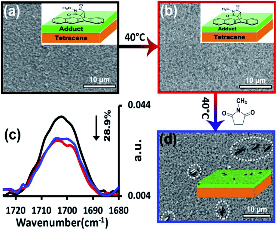 | ||
| Fig. 7 Vapor reconstruction process. (a) SEM image of 100 nm tetracene thin film coated with 7 nm of the standard N-methylmaleimide-tetracene adduct which has been thermally deposited onto the surface. (b) SEM image of the thin film after annealing under N2 at 40 °C for 24 h. (c) PM-IRRAS spectra of 100 nm tetracene thin film coated with 7 nm of the standard N-methylmaleimide-tetracene adduct. Black: after preparation; red: after annealing under N2 at 40 °C for 24 h; blue: after heating with N-methylsuccinimide vapor at 40 °C for 24 h. (d) SEM image of the sample after heating with N-methylsuccinimide vapors at 40 °C for 24 h. All SEM images were taken at an electron energy of 5 keV. | ||
Clearly, the mechanism must be mediated by a small amount of condensate on the surface, which facilitates this morphology change. Because the maleimides, anhydrides, and succinimides are solids at room temperature, the intermolecular forces are substantial (65–75 kJ mol−1).46 These materials can form multilayers of condensate (BET isotherm).47 This could provide a small amount of “solvation” of the product. The presence of condensate can also explain why aggregate formation was limited in the initial 8 hours of the reaction. Here the initial maleic anhydride adsorbing onto the surface primarily undergoes reaction; it is not until the surface is passivated with product that the anhydride could adsorb in quantities sufficient to induce aggregation. Additionally, the mechanism may be broadly applicable to solid–vapor reactions. It is known that solid-phase reactions often experience substantial rate acceleration when exposed to a small amount of vapors of a solvent. This may prove to be the mechanism by which this occurs.44,45
Conclusions
In summary, we have identified many of the morphology features which arise as solid-phase reactions transition from the initial surface reactions to bulk. For the reported Diels–Alder reactions, the asperities formed on the surface were identified as product via infrared and EDX analysis, with these features forming once an initial surface passivation had occurred. Aggregate topography varied greatly depending on whether the studied films were tetracene or pentacene. Formation of these features occurs via a mechanism whereby a small amount of the adsorbate condenses on the surface allowing the product to migrate to form larger aggregates. Topography changes outside of these aggregates (measured via AFM) are minimal. This work explains the initial morphological changes which play a role in all solid-state reactions. From the perspective of generating uniform monolayers on molecular materials, the results suggest that minimizing condensed material (or any solvating material) is critical for forming high quality surfaces.Conflicts of interest
There are no conflicts to declare.Acknowledgements
The authors gratefully acknowledge financial support from the National Science Foundation (NSF), Chemical Structure, Dynamic & Mechanism B Program of the Chemistry Division under Award No. 1665433. This research also utilized a scanning electron microscope, which was funded by the NSF, Major Research Instrumentation (MRI) Program via Award No. 1726994. The authors gratefully acknowledge NT-MDT America for support and would like to thank Marko Surtchev for the AFM imaging and analysis. Thanks to Michael Sayers for his help with manuscript revisions.Notes and references
- P. Brulatti, V. Fattori, S. Muzzioli, S. Stagni, P. Pio Mazzeo, D. Braga, L. Maini, S. Milita and M. Cocchi, J. Mater. Chem. C, 2013, 1, 1823–1831 RSC.
- V. C. Sundar, J. Zaumseil, V. Podzorov, E. Menard, R. L. Willett, T. Someya, M. E. Gershenson and J. A. Rogers, Science, 2004, 303, 1644–1646 CrossRef CAS PubMed.
- S. Thankaraj Salammal, Z. Zhang, J. Chen, B. Chattopadhyay, J. Wu, L. Fu, C. Fan and H. Chen, ACS Appl. Mater. Interfaces, 2016, 8, 20916–20927 CrossRef CAS PubMed.
- S. R. Chemburkar, J. Bauer, K. Deming, H. Spiwek, K. Patel, J. Morris, R. Henry, S. Spanton, W. Dziki, W. Porter, J. Quick, P. Bauer, J. Donaubauer, B. A. Narayanan, M. Soldani, D. Riley and K. McFarland, Org. Process Res. Dev., 2000, 4, 413–417 CrossRef CAS.
- C. Park, J. E. Park and H. C. Choi, Acc. Chem. Res., 2014, 47, 2353–2364 CrossRef CAS PubMed.
- M. A. Gunawan, O. Moncea, D. Poinsot, M. Keskes, B. Domenichini, O. Heintz, R. Chassagnon, F. Herbst, R. M. K. Carlson, J. E. P. Dahl, A. A. Fokin, P. R. Schreiner and J.-C. Hierso, Adv. Funct. Mater., 2018, 28, 1705786 CrossRef.
- J.-C. Hierso, R. Feurer and P. Kalck, Chem. Mater., 2000, 12, 390–399 CrossRef CAS.
- A. G. Walton, The formation and properties of precipitates, REKrieger PubCo, Huntington, N.Y., 1979 Search PubMed.
- H. Ito, M. Muromoto, S. Kurenuma, S. Ishizaka, N. Kitamura, H. Sato and T. Seki, Nat. Commun., 2013, 4, 2009 CrossRef PubMed.
- G. Kaupp, in Organic Solid State Reactions, ed. F. Toda, Springer Berlin Heidelberg, Berlin, Heidelberg, 2005, pp. 95–183 Search PubMed.
- G. Kaupp, J. Phys. Org. Chem., 2008, 21, 630–643 CrossRef CAS.
- G. Kaupp, Comprehensive Supramolecular Chemistry, 1996, vol. 8, pp. 381–423 Search PubMed.
- D. Braga, F. Grepioni, M. Polito, M. R. Chierotti, S. Ellena and R. Gobetto, Organometallics, 2006, 25, 4627–4633 CrossRef CAS.
- D. Braga, M. Cadoni, F. Grepioni, L. Maini and K. Rubini, CrystEngComm, 2006, 8, 756–763 RSC.
- S. Piranej, D. A. Turner, S. M. Dalke, H. Park, B. A. Qualizza, J. Vicente, J. Chen and J. W. Ciszek, CrystEngComm, 2016, 18, 6062–6068 RSC.
- G. J. Deye, J. R. Vicente, S. M. Dalke, S. Piranej, J. Chen and J. W. Ciszek, Langmuir, 2017, 33, 8140–8146 CrossRef CAS PubMed.
- G. J. Deye, J. R. Vicente, J. Chen and J. W. Ciszek, J. Phys. Chem. C, 2018, 122, 15582–15587 CrossRef CAS.
- A. Politano, G. Chiarello, R. Samnakay, G. Liu, B. Gürbulak, S. Duman, A. A. Balandin and D. W. Boukhvalov, Nanoscale, 2016, 8, 8474–8479 RSC.
- O. Bikondoa, C. L. Pang, R. Ithnin, C. A. Muryn, H. Onishi and G. Thornton, Nat. Mater., 2006, 5, 189–192 CrossRef CAS.
- V. E. Henrich and P. A. Cox, The Surface Science of Metal Oxides, Cambridge University Press, Cambridge, 1994 Search PubMed.
- C. M. Perrin and J. A. Swift, CrystEngComm, 2012, 14, 1709–1715 RSC.
- D. J. Gundlach, T. N. Jackson, D. G. Schlom and S. F. Nelson, Appl. Phys. Lett., 1999, 74, 3302–3304 CrossRef CAS.
- S. Lukas, G. Witte and Ch. Wöll, Phys. Rev. Lett., 2001, 88, 028301 CrossRef.
- J. H. Kang and X.-Y. Zhu, Appl. Phys. Lett., 2003, 82, 3248–3250 CrossRef CAS.
- W. S. Hu, Y. T. Tao, Y. J. Hsu, D. H. Wei and Y. S. Wu, Langmuir, 2005, 21, 2260–2266 CrossRef CAS PubMed.
- Y.-Y. Lin, D. I. Gundlach, S. F. Nelson and T. N. Jackson, IEEE Trans. Electron Devices, 1997, 44, 1325–1331 CrossRef CAS.
- V. Kalihari, E. B. Tadmor, G. Haugstad and C. D. Frisbie, Adv. Mater., 2008, 20, 4033–4039 CrossRef CAS.
- R. Ruiz, D. Choudhary, B. Nickel, T. Toccoli, K.-C. Chang, A. C. Mayer, P. Clancy, J. M. Blakely, R. L. Headrick, S. Iannotta and G. G. Malliaras, Chem. Mater., 2004, 16, 4497–4508 CrossRef CAS.
- G. Witte and C. Wöll, J. Mater. Res., 2004, 19, 1889–1916 CrossRef CAS.
- L. Zhou, S. Park, B. Bai, J. Sun, S.-C. Wu, T. N. Jackson, S. Nelson, D. Freeman and Y. Hong, IEEE Electron Device Lett., 2005, 26, 640–642 CAS.
- G. S. Ryu, J. S. Kim, S. H. Jeong and C. K. Song, Org. Electron., 2013, 14, 1218–1224 CrossRef CAS.
- M. Mizukami, N. Hirohata, T. Iseki, K. Ohtawara, T. Tada, S. Yagyu, T. Abe, T. Suzuki, Y. Fujisaki, Y. Inoue, S. Tokito and T. Kurita, IEEE Electron Device Lett., 2006, 27, 249–251 CAS.
- V. Vaidya, S. Soggs, J. Kim, A. Haldi, J. N. Haddock, B. Kippelen and D. M. Wilson, IEEE Trans. Circuits Syst. I Regul. Pap., 2008, 55, 1177–1184 Search PubMed.
- Y. W. Park, H. J. Choi, J. H. Choi, T. H. Park, J.-W. Jeong, E. H. Song and B. K. Ju, IEEE Electron Device Lett., 2012, 33, 1156–1158 CAS.
- M. F. Mabrook, Y. Yun, C. Pearson, D. A. Zeze and M. C. Petty, IEEE Electron Device Lett., 2009, 30, 632–634 CAS.
- B. Ehrler, B. J. Walker, M. L. Böhm, M. W. B. Wilson, Y. Vaynzof, R. H. Friend and N. C. Greenham, Nat. Commun., 2012, 3, 1–6 Search PubMed.
- I. Fleming, Pericyclic reactions, Oxford University Press, Oxford, New York, 1999 Search PubMed.
- T. Breuer, A. Karthäuser and G. Witte, Adv. Mater. Interfaces, 2016, 3, 1500452 CrossRef.
- M. F. Calhoun, J. Sanchez, D. Olaya, M. E. Gershenson and V. Podzorov, Nat. Mater., 2008, 7, 84–89 CrossRef CAS PubMed.
- B. A. Qualizza, S. Prasad, M. P. Chiarelli and J. W. Ciszek, Chem. Commun., 2013, 49, 4495–4497 RSC.
- S. F. Parker, Spectrochim. Acta, Part A, 1995, 51, 2067–2072 CrossRef.
- D. Drouin, A. R. Couture, D. Joly, X. Tastet, V. Aimez and R. Gauvin, Scanning, 2007, 29, 92–101 CrossRef CAS PubMed.
- S. M. Kozlov, F. Viñes and A. Görling, Carbon, 2012, 50, 2482–2492 CrossRef CAS.
- S. Nakamatsu, S. Toyota, W. Jones and F. Toda, Chem. Commun., 2005, 41, 3808–3810 RSC.
- A. Monas, K. Užarević, I. Halasz, M. Juribašić Kulcsár and M. Ćurić, Chem. Commun., 2016, 52, 12960–12963 RSC.
- M. V. Roux, P. Jiménez, M. Á. Martín-Luengo, J. Z. Dávalos, Z. Sun, R. S. Hosmane and J. F. Liebman, J. Org. Chem., 1997, 62, 2732–2737 CrossRef CAS PubMed.
- J. B. Hudson, Surface science: an introduction, Butterworth-Heinemann, Boston, 1992 Search PubMed.
Footnote |
| † Electronic supplementary information (ESI) available: Additional PM-IRRAS spectra, SEM images, EDX mapping, Monte Carlo simulation of EDX spectra, EDX spectra and O quantification. See DOI: 10.1039/c9ra05682c |
| This journal is © The Royal Society of Chemistry 2019 |