DOI:
10.1039/C9RA05503G
(Paper)
RSC Adv., 2019,
9, 27424-27431
Effect of particle sizes and mass ratios of a phosphor on light color performance of a green phosphor thin film and a laminated white light-emitting diode†
Received
17th July 2019
, Accepted 21st August 2019
First published on 2nd September 2019
Abstract
Green phosphor thin films with different silica resin/phosphor mass ratios and phosphor particle sizes were prepared by the hot pressing method. A 405 nm near-ultraviolet light-emitting diode (LED) chip was used to package the laminated white LED (WLED), and the correlated color temperature, luminous efficiency of radiation, light color uniformity, and color coordinate of the laminated WLED were obtained. An increase in the mass ratio and decrease in particle size can effectively affect the scattering coefficient of phosphor photons and the efficiency of the absorption–excitation–emission process, increasing the efficiency and light color uniformity of phosphor thin films and laminated WLEDs. By comprehensive evaluation of various light color parameters, a laminate was prepared with a mass ratio of silica resin/phosphor = 6![[thin space (1/6-em)]](https://www.rsc.org/images/entities/char_2009.gif) :0.75, and the optimum value of the WLED was obtained. According to the IES TM30 standard, its Rf reached 92, Rg reached 101, and Rg and color distortion icons showed increased saturation for green color. Its luminous efficiency of radiation value of 270.21 lm W−1, correlated color temperature of 4423 K, and neutral white characteristics indicate that it is a device suitable for lighting applications.
:0.75, and the optimum value of the WLED was obtained. According to the IES TM30 standard, its Rf reached 92, Rg reached 101, and Rg and color distortion icons showed increased saturation for green color. Its luminous efficiency of radiation value of 270.21 lm W−1, correlated color temperature of 4423 K, and neutral white characteristics indicate that it is a device suitable for lighting applications.
Introduction
A phosphor thin film (PTF) is a type of material that can absorb external excitation photon energy and convert it into a radiation spectrum with specific energy distribution through the transition-radiation process of the activator center.1 PTF is widely used in many fields, such as solar photovoltaic production. After the phosphor is prepared into a film and adhered to the surface of the battery, the converted solar spectrum can effectively improve the utilization efficiency of solar energy.2,3 In the area of a backlit display, after the phosphor materials such as quantum dots are formed into films by spin coating or sputtering, the screen uniformity can be improved.4–6 PTFs also can be used in the phosphor sensing industry and can be applied in such activities as the detection of heavy metal ions Hg2+ and Pb2+, and gas detection of O2, CO2, etc.7–9 In the field of solid-state lighting, the light color uniformity and photothermal stability of white light-emitting diodes (WLEDs) can be improved based on PTFs.10,11
Recently, WLEDs have been widely used in the field of illumination/display. The method of exciting Y3Al5O12:Ce (YAG:Ce) yellow phosphors based on blue chips lacks a red spectrum and exhibits a low light quality. Therefore, a spectral complement is required, such as adding red phosphor. Due to the different phosphor matrixes, there are spectral overlap effects between different phosphors.12–14 A direct hybrid coating will cause re-absorption of the emission spectrum, resulting in the internal consumption of excitation energy. Near-ultraviolet (NUV) LEDs that stimulate blue-green-red tri-primary phosphors are another way to achieve high-quality white light,15,16 and there are more types of phosphors involved. Therefore, a traditional hybrid coating is not suitable for the preparation of NUV WLEDs. According to the spectral characteristics of different phosphors, the laminated PTF is designed to slow the spectral re-absorption effect. Güner17 et al. used blue LEDs to excite red/yellow phosphors as an example. By placing red PTFs on a lower layer of yellow PTFs, the luminous efficiency of WLEDs can be effectively improved. The main reason for this is because the probability of yellow light being absorbed by red phosphors was greatly reduced. In experiments by Fukui18 et al. three primary color PTFs emitted peaks of 450 nm, 530 nm, and 620 nm, and were combined with a 405 nm NUV chip to produce a laminated WLED. When the radiation power was increased by 31.2%, the luminous efficiency could reach 70 lumens per watt (lm W−1), while the color rendering index (Ra) was 95.
Green phosphors are the intermediate layer of the laminated PTF structure. Because the green phosphor emission spectrum is closer to the visual efficiency curve of the human eye than that of the blue and red, parameters such as phosphor conversion efficiency (PCE) and light color uniformity will directly affect the performance of laminated WLEDs. Phosphor particle sizes and mass ratios are the two main factors affecting the performance of PTFs19,20 because they affect the photon scattering direction, absorption–excitation–emission efficiency of PTFs, and the luminous efficiency of radiation (LER), Ra, and light color uniformity of laminated WLEDs.
In this study, the particle sizes and mass ratios of the phosphor in green PTF are two-dimensional variables. Based on the structure of laminated PTF, the package of NUV WLED is realized. The distributions of phosphors in PTF and interface compatibility with the matrix were analyzed by scanning electron microscopy (SEM) and energy-dispersive X-ray spectroscopy (EDS) mapping. The photoluminescence (PL) excitation (PLE) and PL were used to characterize excitation and emission spectra. Based on the Mie scattering theory, the scattering coefficients of the chip emission light (CEL), phosphor emission light (PEL), and the scattering mean free path (SMFP) were calculated. A double integrating sphere (DIS) was used to test and calculate the relationship of two-dimensional variables with the PCE and reflectance/transmittance (R/T). Different types of laminated WLEDs were prepared based on 405 nm NUV LED chips, and the spectral power distribution (SPD) was tested with a NUV-visible-IR spectrometer. A light distribution tester was used to determine the scattering distributions of PEL and CEL in a two-dimensional plane. The color index of laminated WLEDs was evaluated by IES TM30 standard, and multiple indexes such as LER, correlated color temperature (CCT), and color coordinates were combined to obtain the optimal particle size and mass ratio for the laminated WLEDs. The preliminary research on green PTF will lead to further experimentation to develop laminated PTFs and WLEDs. The goal is to study the properties of other color films such as blue and red, and to obtain the effect laws of different primary color PTFs for laminated PTFs and WLEDs, which will provide a reference for the regulation and optimization of light color performance.
Experimental methods
Experimental materials
The laminated PTF and WLED structures are shown in Fig. 1. The chemical compositions of the blue, green, and red phosphors used are (Ba,Sr)10(PO4)6Cl2:Eu2+, (Ba,Sr)2SiO4:Eu2+, and CaAlSiN3:Eu2+, respectively; the corresponding emission spectrum peaks are at 445 nm, 520 nm, and 627 nm, respectively, wherein the central particle diameter D50 of the green phosphor is 27.19 μm, 17.86 μm, and 13.18 μm. Dow Corning MS1002 silica resin was used, with a refractive index of 1.41 at 632.8 nm provided by the supplier Dow Corning Corporation. The NUV LED chip size is 14 mil × 28 mil, peak wavelength is 405 nm, and surface mounted device (SMD) lead frame size is 5.6 mm × 3 mm × 0.7 mm. The mass ratio of silica resin:blue phosphor (S:b-Phosp.) = 6:5.5, silica resin:red phosphor (S:r-Phosp.) = 6:0.25, and the mass ratio of green phosphor is shown in Table 1 below:
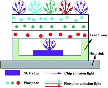 |
| | Fig. 1 Schematic diagram of laminated PTF and WLED. | |
Table 1 Serial numbers (SNs) of green phosphor particle size and mass ratio combination
| D50 (μm) |
6:0.5 |
6:0.75 |
6:1.0 |
6:1.25 |
6:1.5 |
| 27.19 |
A1 |
A2 |
A3 |
A4 |
A5 |
| 17.86 |
B1 |
B2 |
B3 |
B4 |
B5 |
| 13.18 |
C1 |
C2 |
C3 |
C4 |
C5 |
Experimental process
Preparation of PTF. The phosphor and silica resin were weighed according to a preset mass ratio, and stirred at a rotation speed of 200 rpm for 20 minutes to form a colloidal mixture. After completion, the mixture was placed in a vacuum drying oven and deformed at a vacuum of 0.1 MPa for 30 min. In this process, the PTF-forming mold was pre-heated and surface sprayed with a stripping agent. Then, the colloidal mixture was injected into the mold cavity to maintain a temperature of 150 °C, time of 1.5 h, and then, different serial numbers (SNs) of PTF were obtained by cooling the mold.
Preparation of laminated WLEDs. The chip was fixed in the SMD lead frame by solid crystal glue (Kyocera CT285), baked in an oven at 150 °C for 1 h, and the electrode and lead frame were electrically interconnected by a wire bonding machine. A transparent silica resin was injected into the cavity, with the surfaces being maintained at the same level. The PTF was laminated and stacked on the surface of the lead frame in the order illustrated in Fig. 1. The layers of PTF were bonded by transparent silica resin to eliminate the air between the interfaces, and were then baked in an oven at 150 °C for 1.5 h. Finally, the SMD was fixed on an aluminum substrate heat sink by solder paste on a soldering station for heat dissipation to obtain the final laminated WLED.
Test analysis. The microscopic morphology and energy spectrum of PTFs were analyzed using a Zeiss Evo 18 scanning electron microscope and Bruker XFlash 6/30 detector. The condition voltage was 20 kV, the magnification was 4000×, and the excitation and emission spectra were tested by Shimadzu RF6000 spectrophotometer with a xenon lamp at 150 W. The R/T was tested and calculated by Mu-lan DIS, and the diameter of a single sphere was 30 cm. The inner wall was sprayed with BaSO4 power to provide diffuse reflection conditions. The light distribution tester was built by our group, and the components used included a 10 cm diameter integrating sphere, rotating table, and laser. The SPD of the laminated WLED was measured with an Everfine PMS-80 NUV-visible-IR spectrometer with a test range of 380–800 nm. The above tests were performed at room temperature.
Results and discussion
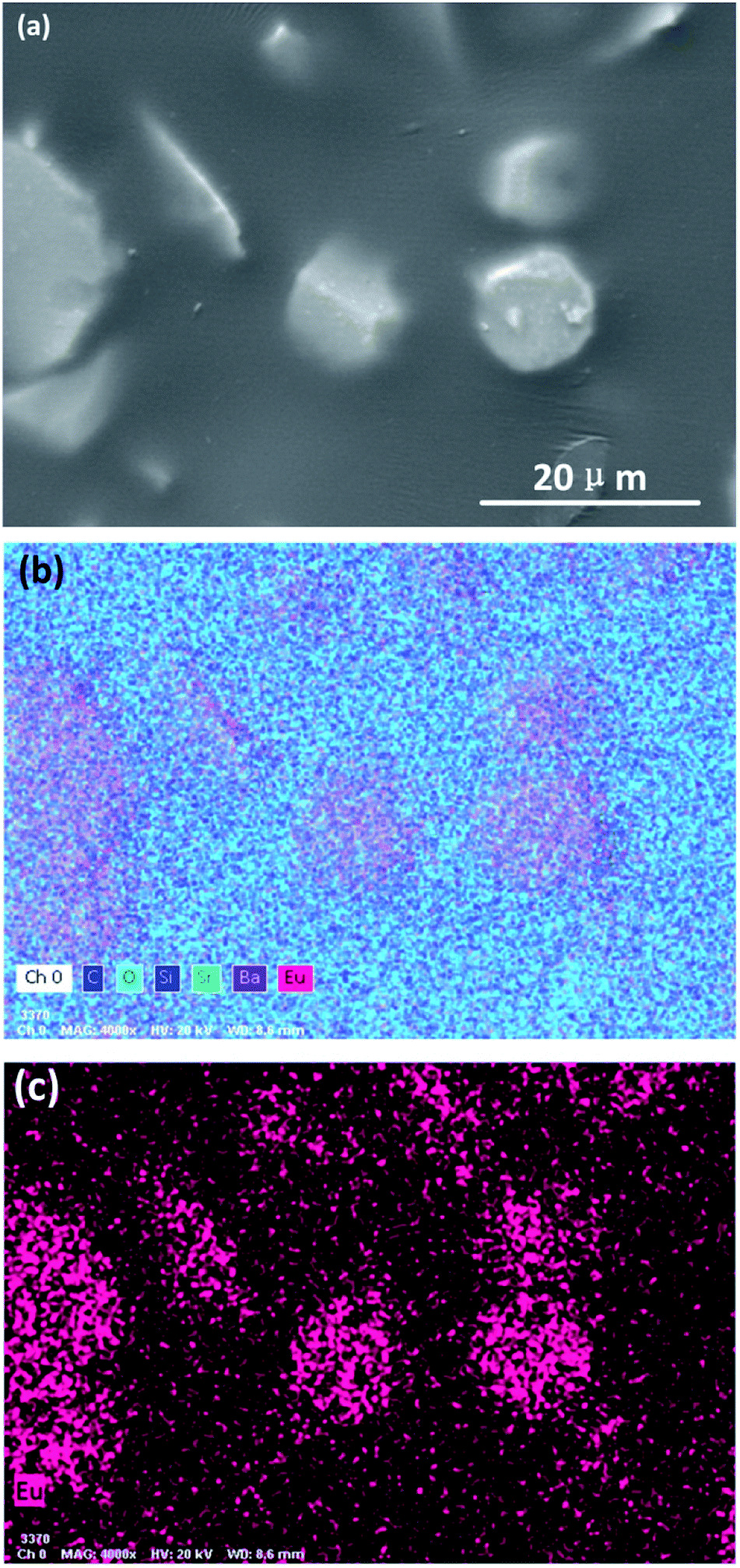
Fig. 2 shows the surface morphology and energy spectrum of the green PTF. The phosphors were evenly distributed in the silica resin matrix, showing an island-like structure. The two-phase interface between the phosphor and silica resin has no obvious channel fault, indicating good interfacial continuity and compatibility, which is due to the coating of the –O–Si–O– flexible macromolecular backbone of the silica resin. The refractive index of the silica resin and phosphor is 1.41 and 1.8,21 respectively. This gradient refractive index facilitates the movement of the converted photons from the surface of the phosphor particles to the silica resin, reducing the probability of total internal reflection (TIR) on the surface of the phosphor. The EDS mapping embodies the elements Ba, Sr, Si, O, and Eu contained in the phosphor. The mapping graphs for different elements are shown in Fig. S1.† The mapping diagram shows that the luminescence center of Eu is evenly distributed in the matrix, and there is no accumulation phenomenon caused by the gravity precipitation of phosphors that facilitates uniform propagation of the emission light.
 |
| | Fig. 2 Green PTF SEM and EDS mapping: (a) SEM, (b) EDS mapping, and (c) Eu2+ mapping. | |
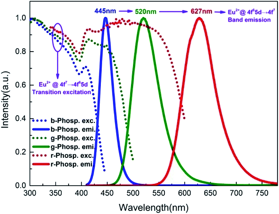
Fig. 3 indicates that all three phosphors have broadband characteristics, which are suitable for the realization of wide-spectrum WLEDs. The 405 nm NUV chip spectrum is included in the phosphor excitation spectrum, and indicates that the three phosphors can be effectively excited by the NUV chip. The luminescence center of the three are all Eu2+, and the electronic configuration is [Xe]4f75s25p6. In the ground state of Eu2+, there are seven electrons that are arranged in the 4f7 configuration, and the ground state spectrum term is 8S7/2. The phosphor excitation spectra are derived from the 4f7 → 4f65d transition of Eu2+, which produces broadband absorption. The emission peaks at 445 nm, 520 nm, and 627 nm correspond to the 4f65d → 4f7 broadband emission of Eu2+. The figure shows that the blue phosphor emission spectrum is completely covered by the excitation ranges of green and red phosphors, and the green phosphor emission spectrum is partially covered by the red phosphor excitation spectrum. This spectral overlap effect results in the phenomenon of re-absorption in the structure by the directly mixed coating. Therefore, based on this phenomenon, the current study used the laminated PTF structure shown in Fig. 1 to reduce the effect of spectral re-absorption on WLED performance.
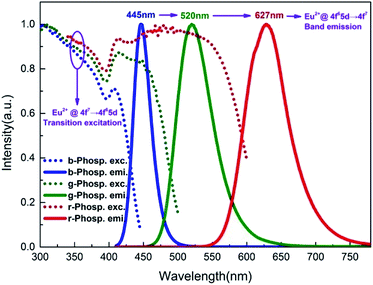 |
| | Fig. 3 Excitation and emission spectra of blue, green, and red phosphors. | |
Fig. 4 shows the scattering distributions of PEL and CEL in a two-dimensional plane under (a) different particles and (b) mass ratios, measured by a light distribution tester (Fig. S2†). The forward and backward distribution of PEL is similar, indicating that the phosphor emission follows the principle of isotropy. There is a selective distribution of CEL, wherein the forward scattering distribution range is significantly larger than that of the backscattering. Fig. 4(a) shows that at the same mass ratio, the scattering distribution range of PEL and CEL increases with the decrease in particle size, which is based on the increase in particle numbers and the scattering probability of the excited phosphor. Fig. 4(b) shows a similar law with the increase in the mass ratio, and because the mass ratio is increased, the particle numbers and scattering amplitude increased accordingly. The increase in the above scattering amplitude can improve the excitation photon scattering and probability of the absorption–conversion process.
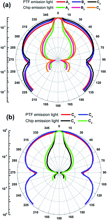 |
| | Fig. 4 Scattering distribution of the emission light on a two-dimensional plane: (a) different particles and (b) different mass ratios. | |
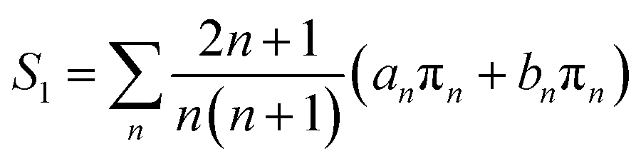
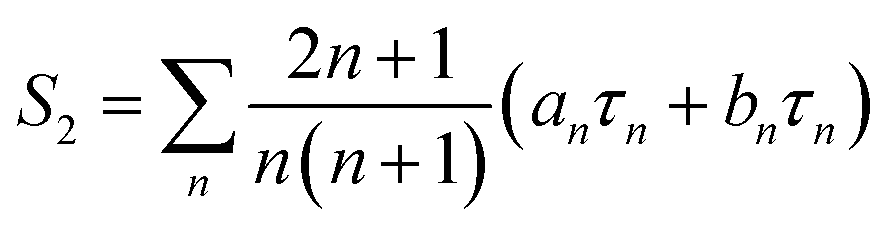
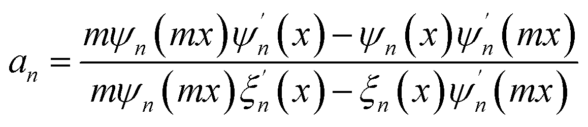
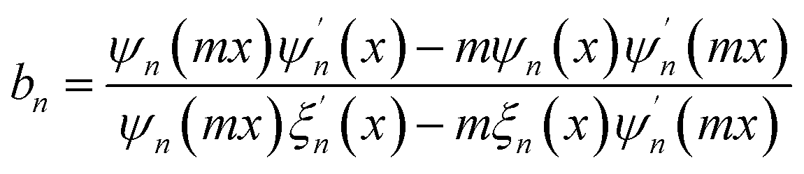
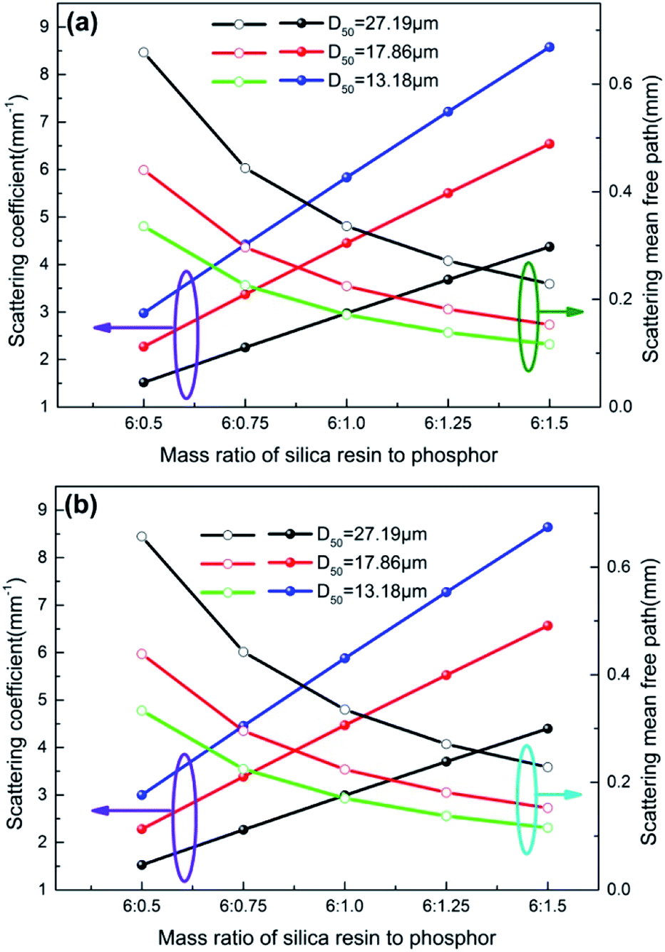
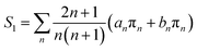
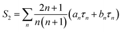
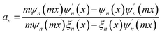
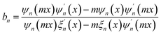
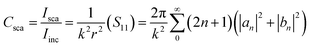
Fig. 5 shows a graph of the SMFP of photon propagation in a PTF and the change trends of the scattering coefficient of PEL and CEL with different mass ratios and particle sizes calculated by the Mie scattering theory; the formula is as follows:22
| |
 | (1) |
| |
 | (2) |
| |
 | (3) |
| |
 | (4) |
| |
 | (5) |
| |
 | (6) |
| |
 | (7) |
Isca and
Iinc denote the intensity of scattered light and incident light,
k denotes the wave number,
r denotes the distance from the particle center to the point on the surface of the scattered light wave,
S1,
S2 denotes the scatter amplitude function,
an,
bn denotes the parity symmetric expansion coefficient, π
n and
τn denote angle coefficients,
x denotes the characteristic size of the particle, and
m denotes the relative refractive index of the particle.
ψn(
x) and
ξn(
x) denote Riccati–Bessel functions,
Csca denotes the scattering cross section,
μsca denotes the scattering coefficient, and
N denotes the number of phosphor particles.
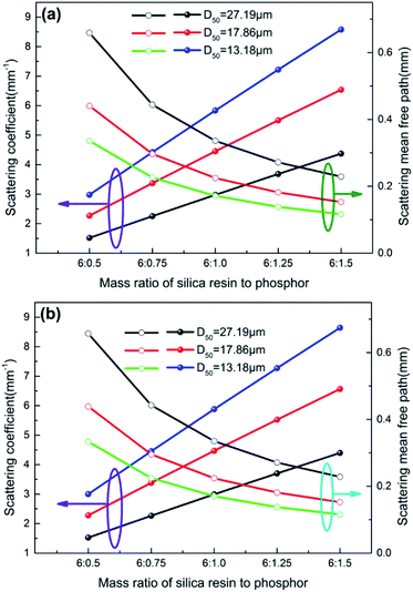 |
| | Fig. 5 Scattering coefficients and MFPs of different emission light: (a) green phosphor and (b) NUV chip. | |
The change trends and amplitude of scattering coefficients and SMFPs for the PEL and CEL are similar, wherein Fig. 5(a) represents the PEL, and Fig. 5(b) represents the CEL. Under the same particle size, the emission light scattering coefficients linearly increase as the proportion of phosphors increase; the main reason for this is the increase in the scattering coefficient. The corresponding SMFP shows a decreasing trend due to a decrease in the spacing between particles. The reduction in SMFP is beneficial for the absorption of excited photons by phosphor particles, and an increase in the excitation probability and conversion efficiency. Then, under the same mass ratio, as the particle size decreases, the scattering coefficient increases and SMFP decreases accordingly, which occurs because the probability of photons being scattered increases and the photon propagation distance between particles is also reduced. This law is similar to that of Fig. 4.
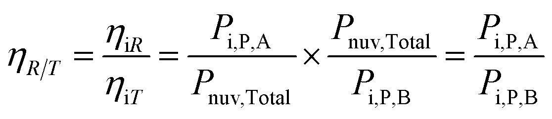
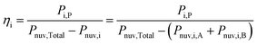
Fig. S3† is a schematic diagram of the DIS test for obtaining the PCE and R/T of PTFs. Laser light is transmitted through a convex lens so that it reaches the surface of the PTF, integrating sphere A and B, which are used to collect the photon energy propagating in the backward and forward directions. The result is displayed by a spectrometer, and the numerical calculation is performed according to the following formula to obtain the desired result:
| | |
Pi,Total = Pi,A + Pi,B (i = nuv, green)
| (9) |
| |
 | (10) |
| |
 | (11) |
Pi,Total (i = nuv, green) denotes the total optical power of a NUV LED and green PTF, respectively;
Pi,A and
Pi,B denote the optical power received in the integrating sphere A and B, respectively; and
ηi,
Pi,P,
Pnuv,i denotes the PCE, which is the optical power of phosphor emission light in green PTF, and the unabsorbed NUV light.
Pnuv,i,A,
Pnuv,i,B and
Pi,P,A,
Pi,P,B denote the optical powers of the NUV and phosphor emission light emitted into the integrating sphere A and B in green PTF, respectively; and
ηR/T,
ηiR,
ηiT denotes the
R/
T, reflectance, and transmittance of the phosphor emission light.
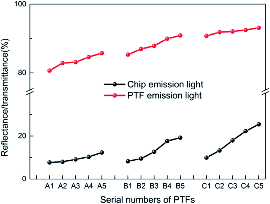
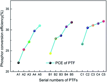
Fig. 6 shows the PCE of PTFs. It can be seen that under the same particle size, the corresponding PCE increases with the increase in the mass ratio. This phenomenon is similar to that of Fig. 4 and 5, and is mainly due to the increase in the particle scattering coefficient and phosphor excitation efficiency. Under the same mass ratio, PCE increases with a decrease in particle size. Fig. 7 is a graph showing the change value of R/T of CEL and PEL, respectively. It can be seen that the value of phosphor is between 80–95%, indicating that the forward propagation mainly dominates. As the mass ratio increases, the value gradually increases due to the increasing composite refractive index of PTFs. When the PEL propagates to the film–air interface, the TIR probability increases due to the refractive index difference, and thus, the corresponding backscattering ratio increases.
 |
| | Fig. 6 PCE of PTFs under different variables. | |
 |
| | Fig. 7 R/T of PTFs under different variables. | |
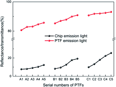
The value of CEL is between 7–30%, indicating that light propagation is dominated by the forward transmission, which follows the Mie scattering theory. As the mass ratio increases, the value of emission light also gradually increases. This is caused by the large absorption of excitation light, especially in the low particle size C group, where it can be seen that as the value is increased, the largest amplitude is observed. This occurs because the particle size of group C is the smallest, and the scattering coefficient is the largest. Thus, the greatest amount of NUV light intensity is absorbed, causing a rapid increase in the value. For small particle sizes, on one hand, the difference between the forward and backward scattered light intensity is not large. On the other hand, due to the large number of particles and scattering coefficients, the scattering effect on the light is also the largest. Therefore, under small particle size conditions, the R/T value approaches a constant, which has little to do with the phosphor ratios.
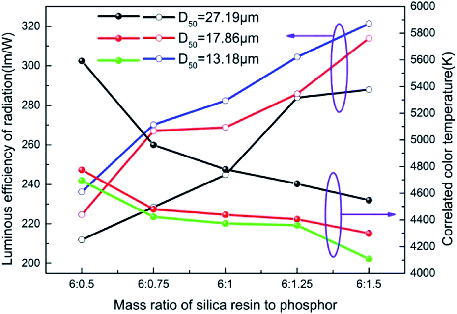
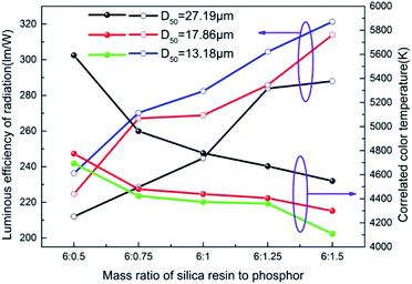
Fig. 8 is a trend diagram of the LER and CCT of the prepared WLED. As the particle size decreases or the phosphor mass ratio increases, the corresponding LER gradually increases, and the CCT gradually decreases. The above rule is consistent with the scattering coefficient and PCE of PTFs. Under the same mass ratio, as the particle size decreases, the scattering coefficient of the phosphor increases, which causes an increase in the phosphor emission intensity so that the LER increases and the CCT decreases. Under the same particle size, as the mass ratio increases, the amount of energy absorbed by the phosphors as the excitation light gradually increases, and therefore, the intensity of the emission light also gradually increases, and the CCT decreases.
 |
| | Fig. 8 LER and CCT trend diagram of laminated WLEDs. | |
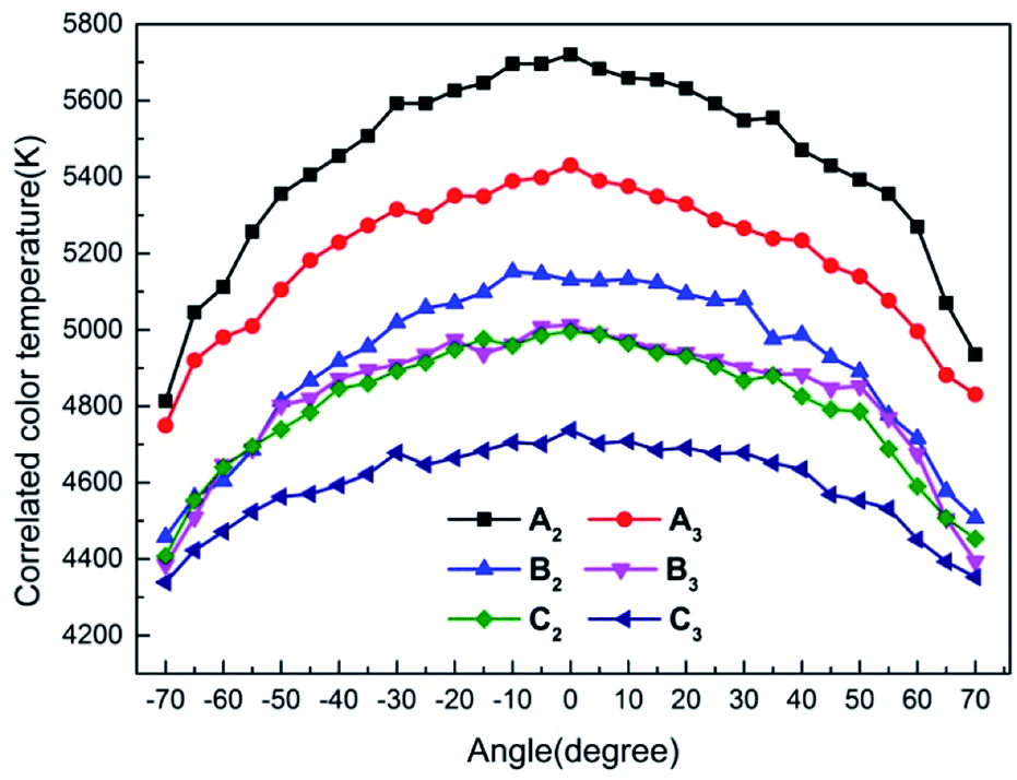
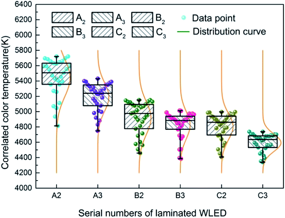
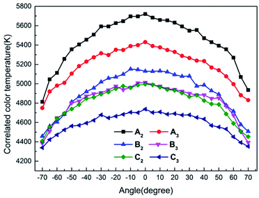
Fig. 9 shows a light scattering distribution of laminated WLEDs on a horizontal two-dimensional plane. The range (R) and standard deviation (SD) values are shown in Table 2, wherein R represents the difference between the maximum and minimum CCT in the bar. It can be seen from the table that the R and SD values decrease with decreasing particle size at the same mass ratio, which is due to the increase in particle numbers and scattering coefficients that increase the probability of photon scattering and the light color uniformity. With the same particle size, as the mass ratio increases, the R and SD values decrease, and the corresponding reason is consistent with the particle size. The box chart in Fig. 10 of the light scattering distribution of laminated WLEDs visually shows the discreteness of the data points, and that the median is gradually decreasing. According to the data from Table 2 and Fig. 10, the optimal value of light color uniformity is in the C3 group.
 |
| | Fig. 9 Light scattering distribution of laminated WLEDs. | |
Table 2 The range and standard deviation values in the different groups
| |
A2 |
A3 |
B2 |
B3 |
C2 |
C3 |
| R |
907 |
682 |
672 |
628 |
589 |
398 |
| SD |
242.42 |
185.21 |
212.67 |
176.91 |
168.24 |
112.99 |
 |
| | Fig. 10 Box chart of the light scattering distribution of laminated WLEDs. | |
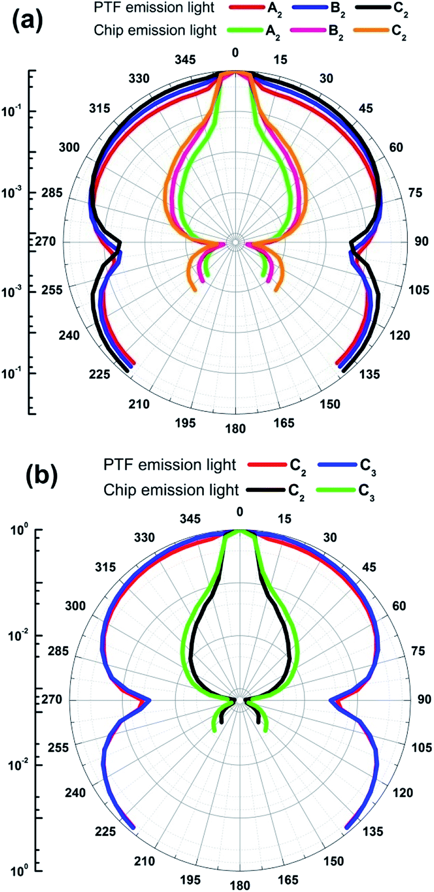
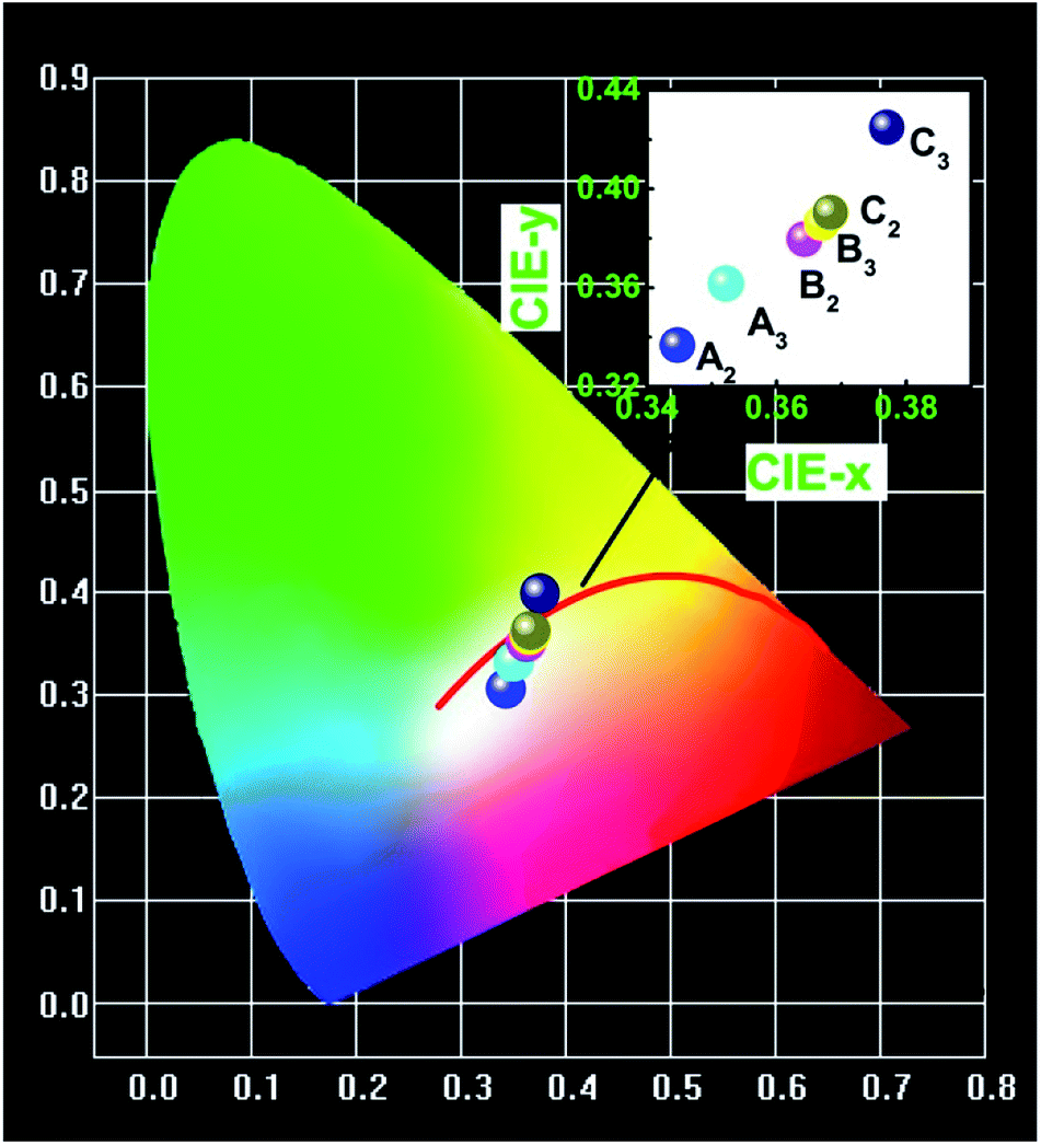
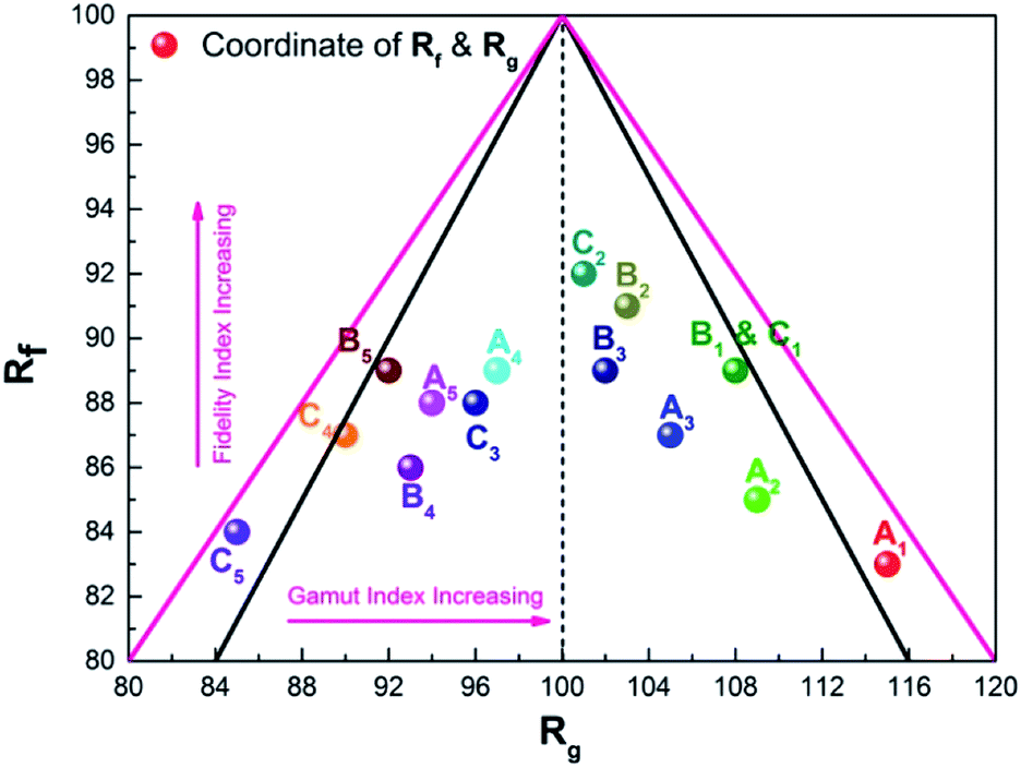
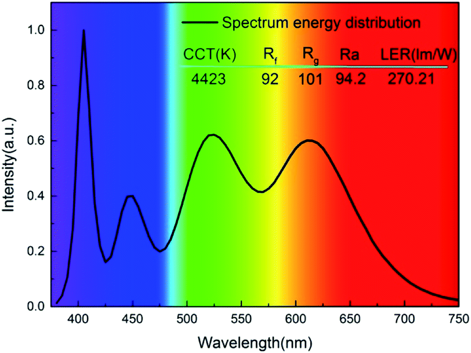
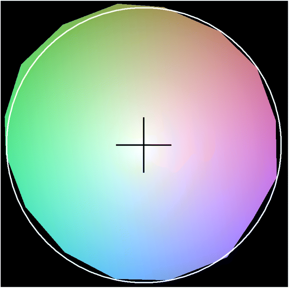
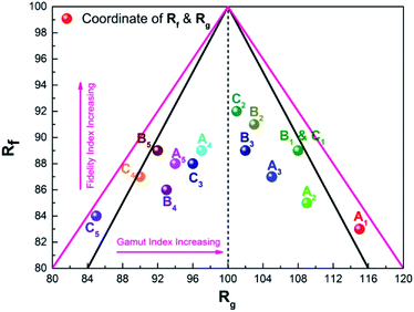
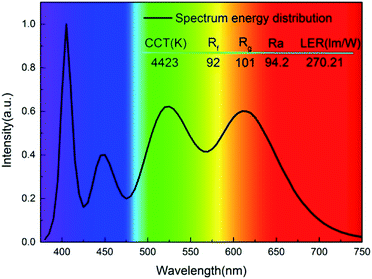
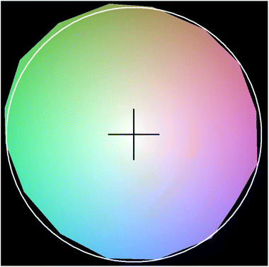
Fig. 11 and 12 show the color coordinates and Rf and Rg coordinates of laminated WLEDs in the A2–C3 and A1–C3 groups, respectively. In Fig. 11, as the mass ratio increases and the particle size decreases, the color coordinates move to the upper right. This is caused by the increase in the green light optical power. The increase in the optical power can improve the LER on the one hand, and also cause the color coordinate of the WLEDs to shift to the upper right green-pink coordinate point, on the other hand. However, if the offset is too large, the color of the emission light will change, and it will deviate from the white light area and shift to another color, such as yellow-green light, which is not suitable for application. The Rf and Rg plot of Fig. 14 is based on the IES TM 30 standard,23,24 where Rf is used to characterize the similarity of each standard color under the illumination of a reference source and a test source (100 represents exactly the same; 0 represents a very large difference). Rg represents the change in the saturation of each standard color (100 represents the same saturation, greater than 100 indicates that the light source can increase the saturation of the color, and below 100 indicates the lower saturation of the color under the test light source), and it can be seen from Fig. 14 that under the premise of Rg > 100, the C2 group has the highest Rf value. In combination with the color coordinate distribution of Fig. 11, the color coordinate is CIE-x = 0.3682, CIE-y = 0.3904, which is closest to the blackbody radiation curve. Therefore, in this series of mass ratio and particle size combination variations, the C2 group is the optimal combination, and the CCT is 4423 K, which corresponds to the laminated WLEDs in the neutral white region. The Ra is as high as 94.2, the Rf is 92, the Rg is 101, the LER is 270.21 lm W−1, and its SPD and color distortion icon is shown in Fig. 13 and 14, respectively. The spectrum is continuously distributed, covering all areas of visible light, while the WLED also can increase the saturation of the green color.
 |
| | Fig. 11 Color coordinates of the laminated WLEDs. | |
 |
| | Fig. 12 Rf and Rg coordinates of the laminated WLEDs. | |
 |
| | Fig. 13 Spectral power distribution of the laminated WLEDs. | |
 |
| | Fig. 14 Color distortion icon. | |
Conclusions
PTFs with different mass ratios and particle sizes were prepared by the hot pressing method. A 405 nm chip was used as the excitation source, and different series of laminated WLEDs were prepared. Particle sizes and mass ratios have an obvious influence on the light color properties (such as scattering distribution, PCEs, and R/Ts) of PTFs and laminated WLEDs based on the scattering effect of phosphor particles. The scattering distribution range of PEL and CEL increased with the decrease in particle size or increase in mass ratio, which is based on the increased scattering probability of the excited phosphor. PCEs and R/Ts showed similar tendencies due to the phosphor scattering effect. Combined with multiple light color indexes, an optimal set of two-dimensional variables was obtained as the C2 group. The corresponding mass ratio of silica resin/phosphor = 6:0.75, the LER of a laminated WLED is 270.21 lm W−1, the CCT is 4423 K, and it has neutral white characteristics. The Ra reached 94.2, the Rf reached 92, and the Rg reached 101, which can increase the saturation of green color. In summary, the WLED device described herein is suitable for lighting applications.
Conflicts of interest
There are no conflicts of interest to declare.
Acknowledgements
The authors would like to acknowledge the financial support in part from the National Key R&D Program of China (Grant No. 2016YFB0400600, 2016YFB0400605) and the Natural Science Foundation of Jiangsu Province (Grant No. BK20171128).
Notes and references
- T. Nakajima, M. Isobe, T. Tsuchiya, Y. Ueda and T. Kumagai, Nat. Mater., 2008, 7, 735–740 CrossRef CAS PubMed.
- W. J. Ho, G. C. Yang, Y. T. Shen and Y. J. Deng, Appl. Surf. Sci., 2016, 365, 120–124 CrossRef CAS.
- C. B. Wang, T. T. Xuan, J. Q. Liu and H. L. Li, Int. J. Appl. Ceram. Technol., 2015, 12, 722–727 CrossRef CAS.
- J. H. Oh, H. J. Kang, M. J. Ko and Y. R. Do, Opt. Express, 2015, 23, A791–A804 CrossRef CAS PubMed.
- S. E. Kim, J. Y. Lee, M. H. Shin and H. J. Kim, IEEE Trans. Electron Devices, 2017, 64, 1153–1160 Search PubMed.
- Y. H. Ko and J. G. Park, J. Korean Phys. Soc., 2018, 72, 45–51 CrossRef.
- S. L. Song, C. X. Chun, Y. Zhao and T. T. Hu, Part. Part. Syst. Charact., 2018, 170047 Search PubMed.
- J. L. Zhang, K. Liu, G. Wang and C. D. Shang, New J. Chem., 2018, 42, 12737–12744 RSC.
- M. V. Kiryukhin, H. H. Lau, S. H. Goh, T. Cathleen, K. Vladimir and S. Anton, Talanta, 2018, 182, 187–192 CrossRef CAS PubMed.
- J. Li, Z. T. Li, G. W. Liang, S. D. Yu, Y. Tang and X. R. Ding, Opt. Express, 2016, 24, 23685–23696 CrossRef CAS PubMed.
- Y. Tang, G. W. Liang, C. J. Song, Z. T. Li, S. D. Yu and X. R. Ding, Mater. Lett., 2018, 227, 104–107 CrossRef CAS.
- S. P. Ying and H. Y. Chien, IEEE Trans. Electron Devices, 2016, 63, 1117–1121 CAS.
- J. S. Lee, P. Arunkumar, S. H. Kim, I. J. Lee, H. Lee and W. B. Im, Opt. Lett., 2014, 39, 762–765 CrossRef CAS PubMed.
- S. P. Ying and J. Y. Shen, Opt. Lett., 2016, 41, 1989–1992 CrossRef CAS PubMed.
- K. J. Choi, J. K. Park, K. N. Kim, C. H. Kim and H. K. Kim, Solid State Phenom., 2007, 124–126, 499–502 CAS.
- Y. Peng, S. Wang, R. Li, H. Li, H. Cheng, M. X. Chen and S. Liu, Appl. Opt., 2016, 55, 4933–4938 CrossRef CAS PubMed.
- T. Güner, D. Köseoğlu and M. M. Demir, Opt. Mater., 2016, 60, 422–430 CrossRef.
- T. Fukui, K. Kamon, J. Takeshita and H. Hayashi, Jpn. J. Appl. Phys., 2009, 48, 112101 CrossRef.
- S. Kim and H. Kim, Opt. Mater., 2018, 75, 814–820 CrossRef CAS.
- C. M. Tan, P. Singh, W. Y. Zhao and H. C. Kuo, Sci. Rep, 2018, 8, 2452 CrossRef PubMed.
- Y. H. Won, H. S. Jang, K. W. Cho, Y. S. Song, D. Y. Jeon and K. Kim, Opt. Lett., 2009, 34, 1–3 CrossRef CAS PubMed.
- M. I. Mishchenko, J. W. Honevier and L. D. Travis, Light Scattering by Nonspherical Particles, Theory, Measurements, and Applications, Academic Press, New York, 2000 Search PubMed.
- A. David, P. Fini, K. W. Houser, Y. Ohno, M. Royer, K. A. G. Smet, M. Wei and L. Whitehead, Opt. Express, 2015, 23, 15888–15906 CrossRef PubMed.
- M. P. Royer, Leukos, 2016, 13, 71–89 CrossRef.
Footnote |
| † Electronic supplementary information (ESI) available. See DOI: 10.1039/c9ra05503g |
|
| This journal is © The Royal Society of Chemistry 2019 |
Click here to see how this site uses Cookies. View our privacy policy here. 
 Open Access Article
 This Open Access Article is licensed under a Creative Commons Attribution-Non Commercial 3.0 Unported Licence
 abc,
Na Zhangbc,
Teng Jiangd,
Peng Chen*a and
Haibo Wang*bc
abc,
Na Zhangbc,
Teng Jiangd,
Peng Chen*a and
Haibo Wang*bc