
 Open Access Article
 This Open Access Article is licensed under a Creative Commons Attribution-Non Commercial 3.0 Unported Licence
Enhancing the performance of perovskite light-emitting devices through 1,3,5-tris(2-N-phenylbenzimidazolyl)benzene interlayer incorporation
Zewu Xiao,
Yanting Wu,
Lihong He,
Xiaoli Yang ,
Yajun Lian,
Guoqing Li and
Xiaohui Yang*
,
Yajun Lian,
Guoqing Li and
Xiaohui Yang*
School of Physical Science and Technology, Southwest University, Chongqing 400715, China. E-mail: xhyang@swu.edu.cn
First published on 16th September 2019
Abstract
Interface engineering is important for enhancing the luminance efficiency and stability of perovskite light-emitting devices. In this work, we study the effects of spin-coated 1,3,5-tris(2-N-phenylbenzimidazolyl)benzene (TPBi) layer incorporation on the crystal structure, morphology, photo-physics, and charge transport characteristics of the underlying MAPbBr3 layer. Introduction of such a TPBi interlayer effectively reduces defect density and increases radiative recombination in the MAPbBr3 layer. Related perovskite light-emitting devices with a TPBi interlayer show a maximum external quantum efficiency of 9.9% and power efficiency of 22.1 lm W−1, which are 2.0 and 1.6 times those of the devices without a TPBi interlayer, respectively. The study provides a simple and effective method to enhance the performance of perovskite light-emitting devices.
Introduction
Organic–inorganic lead halide perovskites are promising for light-emitting devices due to their unique properties such as solution-processability, high luminescence efficiency, good colour purity, and high defect tolerance.1–3 In 2014, Tan et al.4 developed perovskite light-emitting devices with external quantum efficiencies (EQEs) in the range of 0.1–0.8%. Since this report, the performance of perovskite light-emitting devices has advanced rapidly.5–19 At the time of writing, a maximum EQE over 28% has been reported for perovskite light-emitting devices.19A device structure of ITO/hole transport layer/perovskite emission layer/electron transport layer/metal cathode is commonly employed for perovskite light-emitting devices, where ITO is indium tin oxide, the hole transport layer is often poly(3,4-ethylenedioxythiophene):poly(styrenesulfonate) (PEDOT:PSS), and 1,3,5-tris(2-N-phenylbenzimidazolyl)benzene (TPBi) typically serves as the electron transport layer.2,3 Interface engineering is important for enhancing the luminance efficiency and stability of perovskite light-emitting devices. A poly(methyl methacrylate) (PMMA) layer was incorporated between the perovskite emission layer and electron transport layer to balance charge transport, resulting in significant enhancement of device performance.16 You et al.20 showed that the addition of a trioctylphosphine oxide (TOPO) layer reduced defect density in perovskite layers and consequently increased the EQE of related light-emitting devices by 1.2 times. The effects of ethylenediamine (EDA) and polyethyleneimine (PEI) layers on the photo-physics and electroluminescent (EL) properties of the underlying MAPbBr3 layers were compared: EDA-treated MAPbBr3 layers showed improved photoluminescence quantum yields (PLQYs) and EL features over those of the PEI-treated analogues, which was attributed to the fact that the increasing infiltration of EDA with a low molecular weight into MAPbBr3 layers led to the effective defect passivation.21 An elegant “additive nanocrystal pinning” (A-NCP) method using TPBi chloroform solution as the anti-solvent during the film formation process was developed to control the morphology and crystal size of MAPbBr3 films.14 Decreased MAPbBr3 crystal size in the A-NCP samples led to the spatial confinement of electrons and holes and as a result increased electron–hole recombination. N atoms in TPBi possessing a lone electron pair interact with uncoordinated Pb atoms having an empty orbital, forming the Lewis acid–base adduct, which compensates the partial charges and leads to the effective defect passivation.14,22 Both effects contributed to highly efficient perovskite light-emitting devices with a maximum EQE of 8.5%.14 However, it is very demanding to control the preparation parameters to obtain a proper TPBi distribution inside perovskite samples. A solution-processed TPBi electron transport layer was previously used in light-emitting devices based on perovskite nanocrystals.23–25
Herein, we devise incorporation of a spin-coated TPBi layer on MAPbBr3 layers prior to the thermal treatment process based on the following considerations: (1) with the aid of the processing solvents present in the sample, the increasing TPBi infiltration into MAPbBr3 layers promotes defect passivation; (2) possible blocking of electron transport by an insulating layer can be obviated; (3) the process is relatively simple and can be easily controlled. We investigate the effects of spin-coated TPBi layer incorporation on the crystal structure, morphology, photo-physics, and charge transport characteristics of the underlying MAPbBr3 layer. The results indicate that incorporation of such a TPBi interlayer effectively reduces defect density in MAPbBr3 layers, translating into a 2-fold increase in the EQE of related MAPbBr3 light-emitting devices. It is remarkable that EQEs of light-emitting devices are comparable or slightly higher than those of the devices based on A-NCP method.
Results and discussion
Fig. 1a presents schematic configuration of perovskite light-emitting devices, where MAPbBr3 functions as the emission layer, a thin spin-coated TPBi layer as the interface modifier, an evaporated TPBi layer as the electron transport layer, PEDOT:PSS as the hole injection layer, caesium fluoride (CsF) as the electron injection layer, and ITO and aluminium (Al) as the transparent anode and metal cathode. Fig. 1b shows the energy level diagram of the devices, in which the energy levels of the materials and work function of electrodes have been obtained from the literature.2,3 | ||
| Fig. 1 (a) Schematic configuration and (b) energy-level diagram of perovskite light-emitting devices. | ||
Fig. 2 shows top-view scanning electron microscopy (SEM) images of the MAPbBr3 and MAPbBr3/TPBi samples prepared with 0.1, 0.5, or 1 mg ml−1 TPBi solution on the PEDOT:PSS layer, which are denoted as the MAPbBr3, TPBi 0.1, TPBi 0.5, and TPBi 1.0 samples, respectively. All samples show a similar continuous crystalline surface and do not contain obvious voids and cracks. A cross-sectional SEM image of the TPBi 1.0 sample is presented in Fig. 2e. The MAPbBr3 layer is compact and pinhole-free. TPBi layer cannot be resolved from the image because of its small thickness. Fig. 2f and g show atomic force microscopy (AFM) images of the TPBi 1.0 and MAPbBr3/TPBi (2 nm prepared by thermal evaporation) (Evp TPBi) samples. The TPBi 1.0 and Evp TPBi samples show similar morphologies and the root-mean-square (RMS) values of both samples are around 20 nm.
 | ||
| Fig. 2 (a–d) Top-view SEM images of the MAPbBr3, TPBi 0.1, TPBi 0.5, and TPBi 1.0 layers on PEDOT:PSS, insets show the corresponding high-resolution SEM images. (e) A cross-sectional SEM image of the TPBi 1.0 sample. (f and g) AFM images of the TPBi 1.0 and Evp TPBi samples. | ||
As shown in Fig. 3a, the MAPbBr3, TPBi 0.1, TPBi 0.5, and TPBi 1.0 samples show the common diffraction peaks at 15.0°, 30.2°, and 46.1°, which are derived from the respective (100), (200), and (300) crystal planes of the MAPbBr3 cubic crystal structure.26 The TPBi 0.1, TPBi 0.5, and TPBi 1.0 samples exhibit additional diffraction peaks at 21.4°, 34.2°, 37.3°, and 43.4°, originating from the (110), (210), (122), and (220) crystal planes of the MAPbBr3 cubic crystal structure, respectively.26 The appearance of diverse crystal orientations in the TPBi 0.1, TPBi 0.5, and TPBi 1.0 samples is related to the interactions between the TPBi and MAPbBr3 layers. Kim et al.27 reported that the crystal orientation of CH3NH3PbI3 film was varied upon the incorporation of a P3HT:PC61BM overlayer prepared using a similar method in this work. The (100) diffraction peaks of the MAPbBr3, TPBi 0.1, and TPBi 1.0 samples show similar intensities and full-width at half maximum values, as shown in the inset of Fig. 3a.
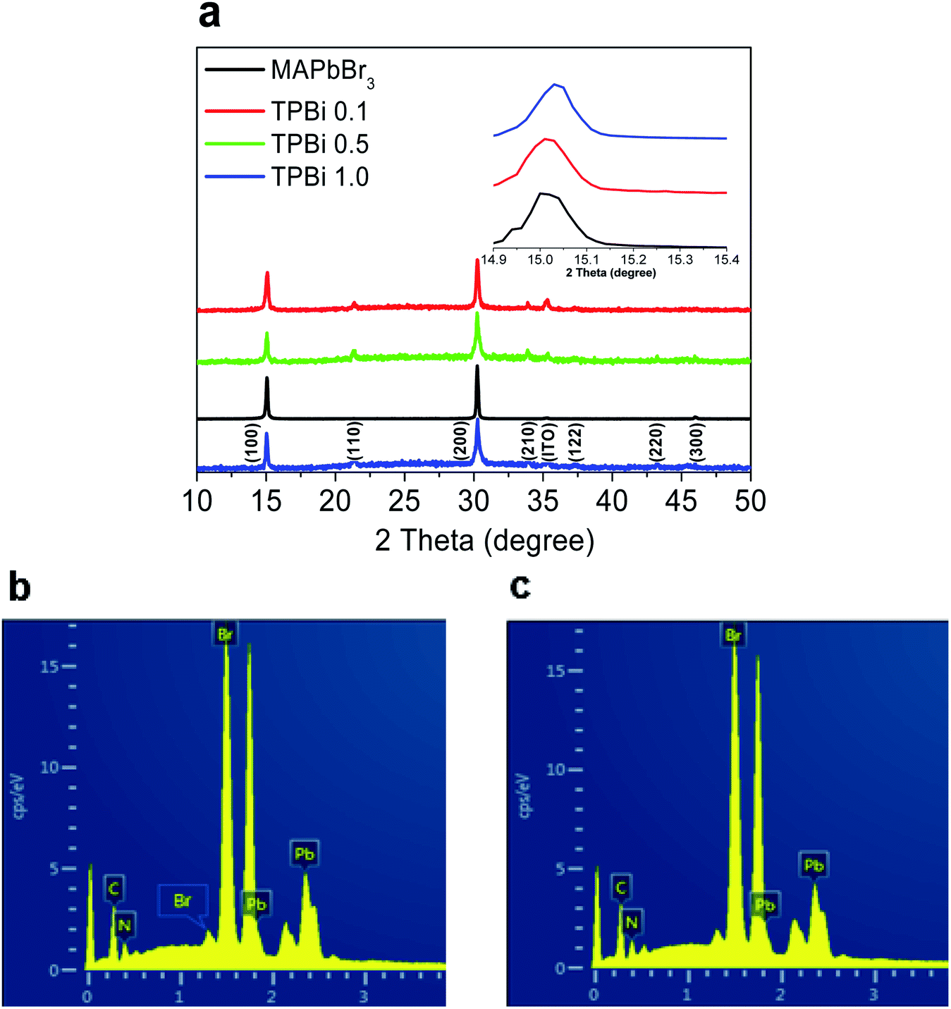 | ||
| Fig. 3 (a) XRD patterns of the MAPbBr3, TPBi 0.1, TPBi 0.5, and TPBi 1.0 samples, the inset shows the enlarged version of the (100) peak region. (b) and (c) EDS measurements of the MAPbBr3 and TPBi 1.0 samples. | ||
We conduct the energy dispersive X-ray spectroscopy (EDS) measurements to study the compositions of the MAPbBr3 and TPBi 1.0 samples, as shown in Fig. 3b and Table 1. The atomic ratios of Pb![[thin space (1/6-em)]](https://www.rsc.org/images/entities/char_2009.gif) :Br and Pb:N are 1:3.1 and 1:1.3 for both samples. As TPBi layer incorporation barely affects the Pb:Br and Pb:N atomic ratios, possible blocking of the MABr escape by a TPBi layer during the thermal treatment process can be excluded.
:Br and Pb:N are 1:3.1 and 1:1.3 for both samples. As TPBi layer incorporation barely affects the Pb:Br and Pb:N atomic ratios, possible blocking of the MABr escape by a TPBi layer during the thermal treatment process can be excluded.
| C | N | Br | Pb | |
|---|---|---|---|---|
| MAPbBr3 | 44.80 | 13.52 | 31.42 | 10.25 |
| TPBi 1.0 | 44.09 | 12.87 | 33.02 | 10.02 |
Fig. 4a shows the UV-vis absorption spectra of the samples. The MAPbBr3, TPBi 0.1, TPBi 0.5, TPBi 1.0, and Evp TPBi samples exhibit a similar absorption profile and absorption onset at ca. 2.27 eV.2 Fig. 4b presents the steady-state photoluminescence (PL) spectra of the samples. Incorporation of a TPBi interlayer increases the PL intensity, which is attributed to the defect healing effect of TPBi.22 The TPBi 1.0 sample shows 1.5–2 times PL intensity compared with that of the MAPbBr3 sample, whereas the Evp TPBi sample exhibits a slight PL intensity increase. PL maxima of the TPBi 0.1, TPBi 0.5, TPBi 1.0, and Evp TPBi samples show a 2–3 nm blue-shift, compared with that of the MAPbBr3 sample, which may be associated with some low-energy traps are filled due to TPBi passivation, leading to blue-shift of the emission wavelength.
 | ||
| Fig. 4 (a) UV-vis absorption and (b) steady-state PL spectra of the MAPbBr3, TPBi 0.1, TPBi 0.5, TPBi 1.0, Evp TPBi, and CB rinsed TPBi 1.0 samples. (c) Time-resolved PL decay curves of the MAPbBr3, TPBi 0.1, TPBi 1.0, and Evp TPBi samples. (d) I–V characteristics of hole-dominated devices containing a MAPbBr3 or CB rinsed TPBi 1.0 layer. | ||
Table 2 shows the PLQYs of the samples. The PLQYs of the MAPbBr3, TPBi 0.1, TPBi 1.0, and Evp TPBi samples are 0.22, 0.26, 0.30, and 0.24, respectively. As the EDS measurements clearly show the Pb:Br atomic ratio of the samples is slightly over-stoichiometric, it can be inferred that there are not a large amount of uncoordinated Pb atoms at the sample surface and the passivation effect of TPBi on surface defects may not be significant. This interpretation is consistent with the PLQY measurement results that the PLQY of the Evp TPBi sample is only slightly higher than that of the MAPbBr3 sample. Conversely, substantially increased PLQY of the TPBi 1.0 sample over that of the MAPbBr3 sample can only be explained by the fact that the increasing TPBi infiltration into the MAPbBr3 layer leads to the effective passivation of defects inside the sample. To verify this interpretation, we rinse the TPBi 1.0 sample with chlorobenzene (the CB rinsed TPBi 1.0 sample) and measure the UV-vis absorption and PL spectra of the sample, which are also included in Fig. 4a and b. The UV-vis absorption spectrum is not changed following the CB rinsing. The PL intensity of the CB rinsed TPBi 1.0 sample is slightly lower than that of the TPBi 1.0 sample, indicating that TPBi molecules trapped inside MAPbBr3 layers, which cannot be easily washed off by CB, play a dictating role in defect remediation.
| τ1 (ns) | A1 (%) | τ2 (ns) | A2 (%) | τave (ns) | PLQY (%) | |
|---|---|---|---|---|---|---|
| MAPbBr3 | 2.92 | 73.33 | 45.58 | 26.67 | 13.33 | 22.1 |
| TPBi 0.1 | 16.91 | 60.50 | 80.69 | 39.50 | 40.67 | 26.7 |
| TPBi 1.0 | 21.74 | 57.90 | 91.57 | 42.10 | 49.05 | 30.1 |
| Evp TPBi | 4.15 | 72.15 | 56.85 | 27.85 | 17.37 | 24.1 |
Fig. 4c shows the time-resolved PL decay curves of the samples. The average life-time of the TPBi 1.0 sample is 49.05 ns, which is significantly longer than that of the MAPbBr3 sample (13.33 ns) and that of the Evp TPBi sample (17.37 ns), indicating that a spin-coated TPBi interlayer incorporation effectively passivates defects and promotes radiative recombination (Table 2).28 Fig. 4d presents I–V characteristics of hole-dominated devices with the structure of ITO/PEDOT:PSS/MAPbBr3 or CB rinsed TPBi 1.0 layer/mCP/MoO3/Ag. Hole-dominated devices containing a MAPbBr3 layer exhibit slightly larger current compared with that of the analogues treated with TPBi, which is probably related to the hole-blocking effect of TPBi infiltrated into MAPbBr3 layers. The combined steady-state PL, PLQY, and time-resolved PL decay measurements indicate that the increasing TPBi infiltration into MAPbBr3 layers promotes defect healing.
Light-emitting devices with a structure of ITO/PEDOT:PSS/MAPbBr3/TPBi interlayer/TPBi/CsF/Al are prepared to examine the effect of TPBi interlayer incorporation on EL properties of MAPbBr3. Light-emitting devices containing the MAPbBr3, TPBi 0.1, TPBi 0.5, and TPBi 1.0 layers are referred to as the MAPbBr3, TPBi 0.1, TPBi 0.5, and TPBi 1.0 devices hereafter. I–V characteristics of the devices shift toward a higher voltage direction with increasing TPBi concentration, which is probably related to decreased hole transport in MAPbBr3 layers upon TPBi layer incorporation (Fig. 4d). The MAPbBr3, TPBi 0.1, TPBi 0.5, and TPBi 1.0 devices show a similar light-emission onset voltage of 2.7 V and luminance values of 7322, 5468, 7063, and 7548 cd m−2 at 6 V, respectively (Fig. 5a). Detailed parameters of the devices are summarized in Table 3.
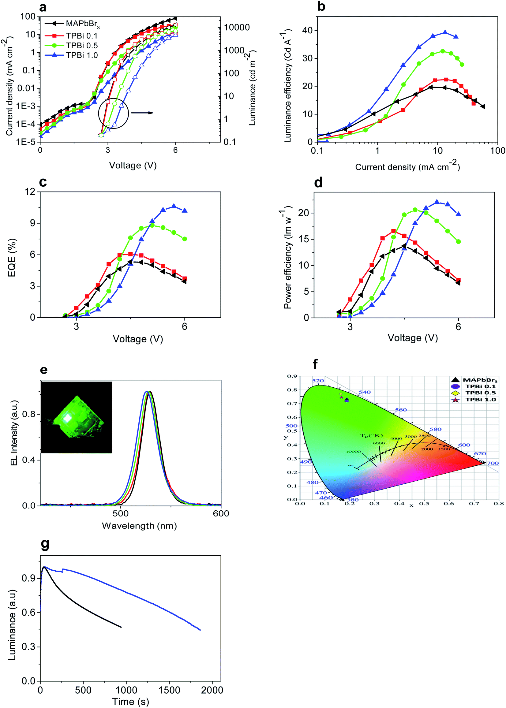 | ||
| Fig. 5 Characteristics of light-emitting devices: (a) V–I–L, (b) luminance efficiency–current density, (c) EQE–V, (d) power efficiency–voltage characteristics, (e) EL spectra, (f) CIE coordinates, and (g) operational stability. Inset of (e) shows a photo of a lit TPBi 1.0 device. | ||
| EQE (%) | LE (cd A−1) | PE (lm W−1) | Lum. @ 6 V (cd m−2) | CIE coordinate | |
|---|---|---|---|---|---|
| MAPbBr3 | 5.0 | 19.7 | 13.7 | 7322 | (0.188, 0.732) |
| TPBi 0.1 | 5.6 | 22.4 | 15.7 | 5468 | (0.189, 0.723) |
| TPBi 0.5 | 8.2 | 32.6 | 20.6 | 7063 | (0.164, 0.771) |
| TPBi 1.0 | 9.9 | 39.2 | 22.1 | 7548 | (0.168, 0.744) |
Fig. 5b and c show luminance efficiency–current density and EQE–voltage characteristics of the devices. The maximum luminance efficiency and EQE of the devices first increase rapidly with increasing TPBi concentration until 0.5 mg ml−1, then elevate slightly with further increase of TPBi concentration from 0.5 to 1 mg ml−1. The maximum EQE of the TPBi 1.0 device is 9.9%, which is ca. 2.0 times that of the MAPbBr3 device and comparable or slightly higher than those of the devices prepared using A-NCP method.14 Fig. 5d presents the power efficiency–voltage characteristics of the devices. The maximum power efficiency of the TPBi 1.0 devices is 22.1 lm W−1, which is ca. 1.6 times that of the MAPbBr3 devices.
EL maxima gradually blue shift with increasing TPBi concentration (Fig. 5e), which is similar to the case in the steady-state PL measurements (Fig. 4b). EL spectra of the MAPbBr3, TPBi 0.1, TPBi 0.5, and TPBi 1.0 devices show full-width at half maximum values of ca. 20 nm, rendering a saturated green emission. Light emission from a TPBi 1.0 device is uniform as shown in the inset of Fig. 5e. The MAPbBr3, TPBi 0.1, TPBi 0.5, and TPBi 1.0 devices show respective Commission Internationale de I'Eclairage (CIE) coordinates of (0.188, 0.732), (0.189, 0.723), (0.164, 0.771), and (0.168, 0.744) (Fig. 5f).
Incorporation of a TPBi interlayer increases the operational stability of light-emitting devices. The operating lifetime (T50) of the TPBi 1.0 devices, measured at 1 mA cm−2 is ca. 30 min, which is longer than that of the MAPbBr3 devices (12.5 min) (Fig. 5g). Increased operational stability of the devices upon spin-coated TPBi interlayer incorporation is related to the reduction of defect density in MAPbBr3 layers. The limited stability of perovskite light-emitting devices is associated with ion migration, which generates defects in perovskite layers and leads to the chemical interactions with charge transport layers and electrodes.29
Conclusions
We study the effects of TPBi interlayer incorporation on the morphology, crystal structure, photo-physics and charge transport properties of the underlying MAPbBr3 layers. The increasing TPBi penetration into MAPbBr3 layers renders the effective defect passivation. As a result, the TPBi interlayer-incorporated devices show a maximum EQE of 9.9%, which are ca. 2 times that of the devices without a TPBi interlayer.Experimental section
Materials
Methylammonium bromide (MABr), lead bromide (PbBr2), 1,3-bis(N-carbazolyl)benzene (mCP), and TPBi were purchased from Xi'an Polymer Technology Corporation (China). Poly(sodium 4-styrenesulfonate) (Na-PSS), dimethylformamide (DMF), chlorobenzene (CB), and PEDOT:PSS were obtained from Sigma-Aldrich and Heraeus Corp. (Germany). All materials were used as received.Device fabrication and characterization
63 mg MABr (0.44 mmol) and 137 mg PbBr2 (0.37 mmol) were dissolved in 1 ml DMF at 60 °C. The MAPbBr3 precursor solution was stirred overnight. TPBi was dissolved in CB with respective concentration of 0.1 mg ml−1, 0.5 mg ml−1, or 1 mg ml−1.ITO substrates were treated with UV–ozone for 30 min. A Na-PSS modified PEDOT:PSS layer30 was spin-coated on the ITO substrates, and the samples were subsequently heated at 170 °C for 10 min to remove water. The MAPbBr3 precursor solution was spin-coated on the PEDOT:PSS layers at 3000 rpm. During the film forming process, 400 μl CB was dripped on the spinning sample to accelerate the crystallization process. TPBi solutions were spin-coated on the perovskite layers. The samples were thermally treated at 60 °C for 20 min and afterwards transferred to a thermal evaporator residing inside a glove box, where 60 nm TPBi, 1 nm CsF, and 200 nm Al were sequentially deposited on the MAPbBr3 layers. The evaporation rates of TPBi, CsF, and Al were 0.03, 0.01, and 0.5 nm s−1, respectively. Hole-dominated devices were accessed by depositing 15 nm mCP, 10 nm MoO3 and 100 nm Ag on the MAPbBr3 layers.
The voltage–current density–luminance (V–I–L) characteristics of the devices were measured with a programmed Keithley 2400 source meter and Konica-Minolta CS-100A chroma meter. EL spectra were recorded with an Ocean Optics USB4000 UV-vis spectrometer. Crystal structure was analyzed by a Rigaku D/Max-B X-ray diffractometer equipped with a Cu Kα radiation source. Surface morphologies were observed by a JSM-7100F field-emission scanning electron microscope (SEM) and Hitachi atomic force microscope (AFM). Steady-state PL spectra and time-resolved PL decay characteristics were collected with an Edinburgh FLS920 spectrophotometer. UV-vis absorption spectra were acquired with a Shimadzu UV-2600 spectrophotometer. PLQYs were measured at an excitation wavelength of 405 nm (I = 5 mW cm−2) following a reported method.31 All measurements were carried out under ambient conditions.
Conflicts of interest
There are no conflicts to declare.Acknowledgements
This work was supported by the National Natural Science Foundation of China (No. 11474232). The authors are indebted to Xuefeng Peng from University of Electronic Science and Technology of China (UESTC) for fruitful discussion.References
- S. D. Stranks and H. J. Snaith, Nat. Nanotechnol., 2015, 10, 391–402 CrossRef CAS PubMed.
- S. A. Veldhuis, P. P. Boix, N. Yantara, M. J. Li, T. C. Sum, N. Mathews and S. G. Mhaisalkar, Adv. Mater., 2016, 28, 6804–6834 CrossRef CAS PubMed.
- L. N. Quan, F. P. G. de Arquer, R. P. Sabatini and E. H. Sargent, Adv. Mater., 2018, 30, 1801996 CrossRef PubMed.
- Z. K. Tan, R. S. Moghaddam, M. L. Lai, P. Docampo, R. Higler, F. Deschler, M. Price, A. Sadhanala, L. M. Pazos, D. Credgington, F. Hanusch, T. Bein, H. J. Snaith and R. H. Friend, Nat. Nanotechnol., 2014, 9, 687–692 CrossRef CAS PubMed.
- A. Sadhanala, S. Ahmad, B. Zhao, N. Giesbrecht, P. M. Pearce, F. Deschler, R. L. Hoye, K. C. Godel, T. Bein, P. Docampo, S. E. Dutton, M. F. deVolder and R. H. Friend, Nano Lett., 2015, 15, 6095–6101 CrossRef CAS PubMed.
- J. Li, S. G. Bade, X. Shan and Z. Yu, Adv. Mater., 2015, 27, 5196–5202 CrossRef CAS PubMed.
- L. Q. Zhang, X. L. Yang, Q. Jiang, P. Y. Wang, Z. G. Yin, H. R. Tan, Y. Yang, M. Y. Wei, B. R. Sutherland, E. H. Sargent and J. B. You, Nat. Commun., 2017, 8, 15640 CrossRef CAS PubMed.
- M. J. Yuan, L. N. Quan, R. Comin, G. Walters, R. Sabatini, O. Voznyy, S. Hoogland, Y. B. Zhao, E. M. Beauregard, P. Kanjanaboos, Z. H. Lu, D. H. Kim and E. H. Sargent, Nat. Nanotechnol., 2016, 11, 872–877 CrossRef CAS PubMed.
- N. N. Wang, L. Cheng, R. Ge, S. T. Zhang, Y. F. Miao, W. Zou, C. Yi, Y. Sun, Y. Cao, R. Yang, Y. Q. Wei, Q. Guo, Y. Ke, M. T. Yu, Y. Z. Jin, Y. Liu, Q. Q. Ding, G. C. Xing, H. Tian, C. H. Jin, F. Gao, R. H. Friend, J. P. Wang and W. Huang, Nat. Photonics, 2016, 10, 699–704 CrossRef CAS.
- Y. K. Chih, J. C. Wang, R. T. Yang, C. C. Liu, Y. C. Chang, Y. S. Fu, W. C. Lai, P. Chen, T. C. Wen, Y. C. Huang, C. S. Tsao and T. F. Guo, Adv. Mater., 2016, 28, 8687–8694 CrossRef CAS PubMed.
- Z. G. Xiao, R. A. Kerner, L. F. Zhao, N. L. Tran, K. M. Lee, T. W. Koh, G. D. Scholes and B. P. Band, Nat. Photonics, 2017, 11, 108–115 CrossRef CAS.
- Q. Wang, J. Ren, X. F. Peng, X. X. Ji and X. H. Yang, ACS Appl. Mater. Interfaces, 2017, 9, 29901–29906 CrossRef CAS PubMed.
- P. Chen, Z. Y. Xiong, X. Y. Wu, M. Shao, Y. Meng, Z. H. Xiong and C. H. Gao, J. Phys. Chem. Lett., 2017, 8, 3961–3967 CrossRef CAS PubMed.
- H. Cho, S. H. Jeong, M. H. Park, Y. H. Kim, C. Wolf, C. L. Lee, J. H. Heo, A. Sadhanala, N. S. Myoung and S. Yoo, Science, 2015, 350, 1222–1225 CrossRef CAS PubMed.
- X. Liu, X. Y. Gong, Y. Lv, Y. S. Hu, Y. Fan, J. Lin, X. M. Liu and X. Y. Liu, Adv. Opt. Mater., 2018, 6, 1801245 CrossRef.
- K. Lin, J. Xing, L. N. Quan, F. P. G. de Arquer, X. Gong, J. Lu, L. Xie, W. Zhao, D. Zhang, C. Yan and W. Li, Nature, 2018, 562, 245–248 CrossRef CAS PubMed.
- Y. Cao, N. Wang, H. Tian, J. Guo, Y. Wei, H. Chen, Y. Miao, W. Zou, K. Pan and Y. He, Nature, 2018, 562, 249–253 CrossRef PubMed.
- S. Q. Wang, S. L. Zhao, Z. Xu, D. D. Song, B. Qiao, H. X. Yue, J. Yang, X. G. Zheng and P. Wei, Appl. Phys. Lett., 2018, 113, 213501 CrossRef.
- Y. Shen, L. P. Cheng, Y. Q. Li, W. Li, J. D. Chen, S. T. Lee and J. X. Tang, Adv. Mater., 2019, 31, 1901517 CrossRef PubMed.
- X. Yang, X. Zhang, J. Deng, Z. Chu, Q. Jiang, J. Meng, P. Wang, L. Zhang, Z. Yin and J. You, Nat. Commun., 2018, 9, 570 CrossRef PubMed.
- S. Lee, J. H. Park, B. R. Lee, E. D. Jung, J. C. Yu, D. D. Nuzzo, R. H. Friend and M. H. Song, J. Phys. Chem. Lett., 2017, 8, 1784–1792 CrossRef CAS PubMed.
- M. H. Park, S. H. Jeong, H. K. Seo, C. Wolf, Y. H. Kim, H. Kim, J. Byun, J. S. Kim, H. Cho and T. W. Lee, Nano Energy, 2017, 42, 157–165 CrossRef CAS.
- X. Zhang, H. Lin, H. Huang, C. Reckmeier, Y. Zhang, W. C. H. Choy and A. L. Rogach, Nano Lett., 2016, 16, 1415–1420 CrossRef CAS PubMed.
- J. Mao, H. Lin, F. Ye, M. Qin, J. M. Burkhartsmeyer, H. Zhang, X. Lu, K. S. Wong and W. C. H. Choy, ACS Nano, 2018, 12, 10486–10492 CrossRef CAS PubMed.
- H. Huang, H. Lin, S. V. Kershaw, A. S. Susha, W. C. H. Choy and A. L. Rogach, J. Phys. Chem. Lett., 2016, 7, 4398–4404 CrossRef CAS PubMed.
- Y. H. Kim, H. Cho, J. H. Heo, T. S. Kim, N. S. Myoung, C. L. Lee, S. H. Im and T. W. Lee, Adv. Mater., 2015, 27, 1248–1254 CrossRef CAS PubMed.
- Y. L. Liu, I. S. Shin, Y. C. Ma, I. K. Hwang, Y. K. Jung, J. W. Jang, J. H. Jeong, S. H. Park and K. H. Kim, ACS Appl. Mater. Interfaces, 2018, 10, 31366–31373 CrossRef CAS PubMed.
- J. Chen and N. J. Park, Adv. Mater., 2018, 30, 1803019 CrossRef PubMed.
- G. Grancini and M. K. Nazeeruddin, Nat. Rev. Mater., 2019, 4, 4–22 CrossRef CAS.
- X. F. Peng, X. Y. Wu, X. X. Ji, J. Ren, Q. Wang, G. Q. Li and X. H. Yang, J. Phys. Chem. Lett., 2017, 8, 4691–4697 CrossRef CAS PubMed.
- N. C. Greenham, I. D. W. Samuel, G. R. Hayes, R. T. Phillips, Y. A. R. R. Kessener, S. C. Moratti, A. B. Holmes and R. H. Friend, Chem. Phys. Lett., 1995, 241, 89–96 CrossRef CAS.
| This journal is © The Royal Society of Chemistry 2019 |