
 Open Access Article
 This Open Access Article is licensed under a Creative Commons Attribution-Non Commercial 3.0 Unported Licence
Spacer layer design for efficient fully printable mesoscopic perovskite solar cells†
Tongfa Liu a,
Yuli Xiong*b,
Anyi Meic,
Yue Huc,
Yaoguang Rongcd,
Mi Xuc,
Zheng Wanga,
Lingyun Loua,
Dongjie Dua,
Shizhao Zhenga,
Xia Longa,
Shuang Xiaoa,
Shihe Yang*ae and
Hongwei Han*c
a,
Yuli Xiong*b,
Anyi Meic,
Yue Huc,
Yaoguang Rongcd,
Mi Xuc,
Zheng Wanga,
Lingyun Loua,
Dongjie Dua,
Shizhao Zhenga,
Xia Longa,
Shuang Xiaoa,
Shihe Yang*ae and
Hongwei Han*c
aGuangdong Provincial Key Laboratory of Nano-Micro Materials Research, School of Chemical Biology & Biotechnology, Peking University Shenzhen Graduate School, Shenzhen, P. R. China. E-mail: chsyang@pku.edu.cn
bHubei Province Engineering Research Center for Intelligent Micro-nano Medical Equipment and Key Technologies, Wuhan Textile University, Wuhan, Hubei, P. R. China. E-mail: y.xiong@wtu.edu.cn
cMichael Grätzel Center for Mesoscopic Solar Cells, Wuhan National Laboratory for Optoelectronics, China-EU Institute for Clean and Renewable Energy, Huazhong University of Science and Technology, Wuhan, Hubei, P. R. China. E-mail: hongwei.han@mail.hust.edu.cn
dSchool of Physics and Optoelectronics Engineering, Nanjing University of Information Science and Technology, Nanjing, Jiangsu, P. R. China
eDepartment of Chemistry, The Hong Kong University of Science and Technology, Clear Water Bay, Kowloon, Hong Kong 999077, P. R. China
First published on 20th September 2019
Abstract
The spacer layer is a key component of fully printable mesoscopic perovskite solar cells, but its precise characteristics are far from being understood in relation to the device design. In the present work, we perform a detailed systematic study on the effects of spacer parameters, such as size of building blocks, layer thickness, etc., on properties of the perovskite filler, insulating ability and performance of fully printable mesoscopic perovskite solar cells by combining the techniques of time-resolved photoluminescence, high-resolution TEM, insulating resistance measurements, impedance spectroscopy and J–V characteristics. Drawing on the deep understanding from these studies, we formulate key principles, which are anticipated to guide the design of the advanced spacer layer for fully printable mesoscopic perovskite solar cells.
Lead halide perovskite (PVSK) as a promising semiconducting material has been introduced as a light harvesting semiconductor because of its ease of fabrication and excellent physical properties, such as tunable bandgap, strong absorbance, long carrier diffusion length and shallow intrinsic trap state level.1–9 Extremely flat and compact perovskite thin film with large crystal size has gained particular attention to boost power conversion efficiency (PCE) by sequential deposition method, vapor deposition, solvent-annealing, solvent engineering, hot-casting method, intramolecular exchange methods, and additive, etc.10–16 Benefiting from rapid improvements in formation of high quality perovskite thin film, a certified PCE of 25.2% has been achieved.17 However, illumination stability in real environment still remains a serious challenge due to the inherent moisture and UV sensitivity of perovskite. Moreover, using expensive and rare metals as back contact, such as gold and silver, may limit large-scale production in the future. As the competing architecture of perovskite solar cells, TiO2/spacer/carbon (abbreviated as TSC) films based fully printable mesoscopic perovskite solar cells (FP-MPSC) have attracted a lot of researchers due to their low cost and printable large-scale production process.18–21 In this type of solar cell, carbon can efficiently collect hole from perovskite layer even without any other hole transporting materials.22,23 Most importantly, FP-MPSC could work with excellent illumination stability and heat-stress stability by filling TSC films with (5-AVA)xMA1−xPbI3 (5-AVA = 5-aminovaleric acid, MA = methylammonium), although the efficiency of 12.8% is still far behind from the most efficient solar cell.16,21,24
Spacer, as an important part of FP-MPSC, plays a crucial role in obtaining high performance device. Basically, the spacer layer mainly burdens triple important tasks in the efficient mesoscopic perovskite solar cells. Firstly, the core function of spacer is to separate anode and cathode and to prevent electrons in TiO2 from transporting directly to carbon electrode. The separating property of spacer depends on spacer particle sizes, morphology, materials, etc. This requires that spacer layer has no cracking and has wide bandgap. Secondly, the perovskite confined in the mesopores of spacer layer can absorb photons transmitted through perovskite/TiO2 composite layer and have contribution to photocurrents. Thirdly, the holes produced in the perovskite/TiO2 composite layer have to go through perovskite/spacer composite layer to reach carbon electrode. And the electrons produced in the perovskite/spacer composite layer have to go through perovskite/spacer composite layer to reach TiO2 electrode. Because spacer layer has these important functions, some research on spacer layer have been carried out. Recently, Al2O3 or ZrO2 spacer layer was compared with respect to their pore size.25 However, conclusion of the effect of pore size in two different materials was incomplete. The effect of spacer layer thickness was simply discussed both in monolithic dye-sensitized solar cells and FP-MPSC.20,26 The morphology of spacer layer was also improved to increase PCE of FP-MPSC.27 Although these researches made some progress, there are no clear standards that what should an ideal spacer layer satisfy. Therefore, it is urgent to carry out detailed study on how the parameters of spacer affect the above functions and performance of mesoscopic printable perovskite solar cells.
In the present study, the effects of size of building blocks of spacer layer, thickness of spacer layer on property of perovskite crystals, insulating property, and performance of mesoscopic perovskite solar cells were investigated in details. Based on these deep understandings, critical principles to design advanced spacer layer are proposed.
ZrO2 is used as spacer material due to its large band gap and high conduction band energy level. There are five different sizes of spacer building blocks in this study. The average particle sizes of spacer are measured to be about 5 nm, 10 nm, 20 nm, 60 nm and 100 nm, respectively, and hereafter referred to as S5, S10, S20, S60, S100 spacer, respectively. SEM images of as-prepared spacer films using these building blocks are shown in Fig. 1. X-ray diffraction patterns of spacer film with different particle sizes are presented in Fig. 1f, indicating that the five spacer films were all tetragonal crystal phase as majority phase. From Scherrer equation, the crystal sizes of spacer building blocks were calculated to be about 5 nm, 10 nm, 20 nm, 30 nm, 30 nm, respectively. These results indicated that the S60 and S100 particles are consisted of 30 nm sized crystal ZrO2. Fig. 1 presents that there is a large difference in surface morphology with particle size increasing. There are cracks in S5 and S10 spacer films and micrometer scale pores exist in the S100 spacer, while the surface of S20 and S60 are very uniform without defects.
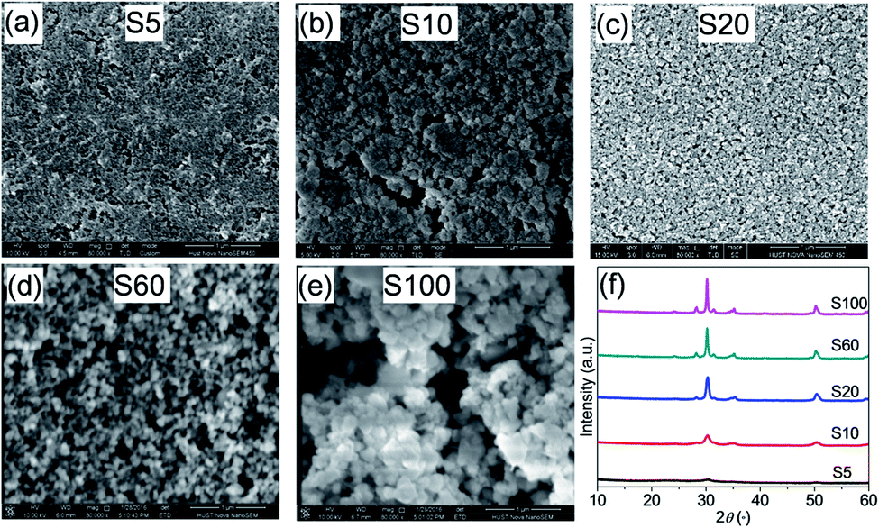 | ||
| Fig. 1 SEM images of spacer films with particle size of 5 nm (a), 10 nm (b), 20 nm (c), 60 nm (d) and 100 nm (e), respectively. (f) XRD patterns of spacer film with different building block sizes. | ||
During solvent evaporation of perovskite precursor, perovskite crystal growth is restricted by randomly interconnected mesopores of spacer film, leading to nanoscale crystal size and random crystal orientation, as observed by high resolution transmission electron microscope (Fig. 2a), in which clear crystal lattices of perovskite crystals can be distinguished from spacer particles. Meanwhile, the mesopores of spacer film is fulfilled with perovskite materials, providing continuous channels for charge carriers. The crystal size of perovskite material in spacer film is strongly influenced by mesopore size of spacer layer, as seen in XRD intensity of perovskite at 2θ of about 14.2° (Fig. 2b). There is an apparent trend that the intensity increased with increasing the particle size of spacer film. As a reference, perovskite was also deposited on bare glass, which exhibited the best crystallinity. The calculated sizes of perovskite from XRD spectra are 4.3 nm, 3.9 nm, 6.2 nm, 11.5 nm, and 12.6 nm, respectively, for the S5, S10, S20, S60, and S100 spacer layer. Apparently, the sizes of perovskite crystals confined in the spacer layer are smaller than the average pore sizes of spacer layer measured by N2 absorption/desorption isotherms (Table S1†). The high-resolution TEM image also gives consistent results. For example, the sizes of perovskite crystals confined in the S20 spacer layer are between 8.4 nm to 12.7 nm measured in the TEM image (Fig. 2a). The infiltrated perovskite started to nucleate onto the heterogeneous surface of spacer building blocks with high surface area, resulting to multiple nucleation centers and small crystal size. In order to evaluate the effect of spacer particle size on physiochemical properties of perovskite, the band-edge emission spectra of perovskite/spacer composite film were measured in Fig. 2c. The band-edge emission spectrum of perovskite deposited on bare glass peaked at 762 nm (with photon energy of 1.627 eV). As the particle size of spacer film decreased, a blue shift of the band-edge photoluminescence occurred, and linewidth broadened. The peak position of perovskite emission spectra can be tuned in the range of 33 nm through varying the pore size of spacer film. The increase of emission line width at grain boundaries can be attributed to disorder and defects of perovskite,14,15 which also led to the decrease of lifetime in time-resolved PL (Fig. 2d). Perovskite film grown on glass has the lifetime of 141.9 ns. However, perovskite grown in spacer film decreased to 0.5 ns, 8.4 ns, 24.1 ns, 37.2 ns, 53.7 ns, for S5, S10, S20, S60, S100, respectively.
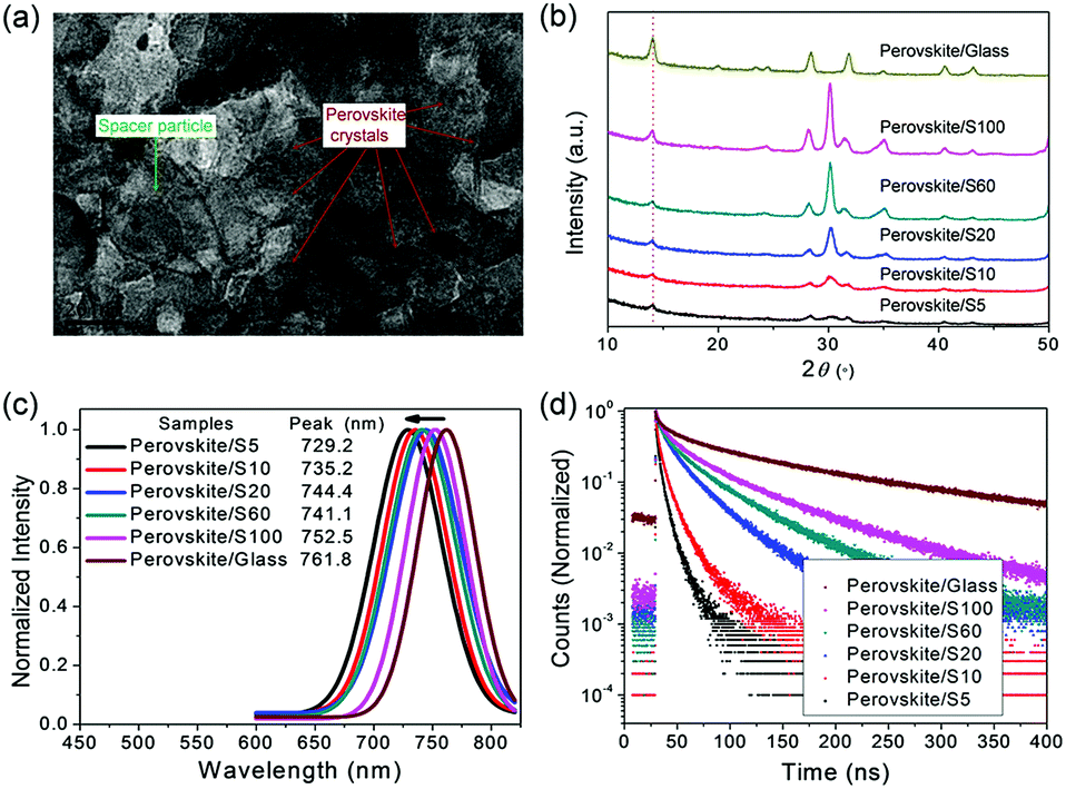 | ||
| Fig. 2 (a) High resolution transmission electron microscope image of perovskite/S20 spacer film composite. (b) XRD of perovskite/spacer film composite. (c) Steady PL emission spectra and (d) time-resolved PL of perovskite/spacer film composite. | ||
The particle size of spacer also has large effect on insulating ability of spacer films with the same thickness. FTO/spacer/carbon configuration was designed to measure the insulating ability of spacer layers. In ideal conditions, the resistance between carbon and FTO, defined as insulating resistance (RI), should be infinite, indicating that there is not any leakage current from ideal insulating spacer. However, all of the measured resistance has finite values, summarized in Table 1, from 300 Ω to 1.5 kΩ. There are clear trends of insulating resistance with particle sizes of spacer. The S100 spacer film has lowest insulating resistance, indicating the poorest insulating ability. It was found that the S100 spacer film was very loosely packed even after sintering at 500 degrees for one hour. The sintered S100 spacer film could be easily peeled off from substrate using 3M Scotch tape. In contrast, S5 and S10 spacer films were much more robust than other spacer films to be peeled off from the substrate after sintering at 400 degrees for one hour. This difference in spacer film about peeling strength was resulted from sintering energetics and was originated from quantum size effect dominated by surface to bulk atom ratio of spacer building block nanocrystals.28–31
| Spacer | Lifetime (ns) | RI (Ω) | JSC (mA cm−2) | VOC (mV) | FF (%) | PCE (%) |
|---|---|---|---|---|---|---|
| No spacer | — | 30 | 16.21 | 605 | 66 | 6.52 |
| S5 | 0.5 | 1500 | 16.06 | 871 | 67 | 9.42 |
| S10 | 8.4 | 970 | 18.26 | 908 | 71 | 11.77 |
| S20 | 24.1 | 960 | 19.10 | 871 | 71 | 11.86 |
| S60 | 37.2 | 800 | 18.19 | 865 | 70 | 11.08 |
| S100 | 53.7 | 300 | 18.62 | 808 | 67 | 10.10 |
Fig. 3a is the scheme showing the layout of FP-MPSC. The influence of the size of spacer layer building block on the photocurrent density–voltage (J–V) curves of the (5-AVA)xMA1−xPbI3 perovskite devices without and with spacer layer was evaluated in Fig. 3b and photovoltaic parameters are summarized in Table 1. FP-MPSC without spacer was studied as the reference device. The device without spacer film has a relatively low efficiency of 6.52%, featuring very low open-circuit voltage (VOC) of 605 mV, which is consistent with previous result for the devices using two-step method deposited MAPbI3 perovskite.20 The VOC increased significantly from 605 mV to above 808 mV, when the device added spacer layers. The device with S100 spacer, which had best crystallinity and longest photoluminescence lifetime, is expected to have excellent performance. But S100 spacer has relatively low VOC of 808 mV and low PCE of 10.10%. This is resulted from poorest insulating ability of S100 spacer among these spacer films. Balancing from photoluminescence property of perovskite confined in spacer layer and insulating property of spacer layer, 20 nm-sized S20 spacer film had the best performance with efficiency of 11.86%. It is common sense that devices with large perovskite crystal size with low trap density can approach VOC to the limit of theoretical value.1,32,33 The blue shift of the band-edge photoluminescence and decreased lifetime of perovskite in spacer film may explain the relatively low VOC (less than 1.0 V) relative to conventional planar perovskite solar cells (VOC was more than 1.1 V) in which the size of perovskite crystal was larger than 500 nm. Spacer film with large pore size and excellent insulating property are expected to further improve VOC of FP-MPSC. The observed quantum size effect of perovskite nanocrystals confined in spacer mesopores in some extents results from templating effect of spacer nanoparticles and unmatched crystal lattices. Matched crystal lattices may mitigate the quantum size effect by heteroepitaxy via reduced nucleation density.34
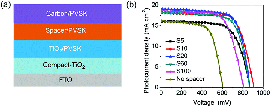 | ||
| Fig. 3 (a) Scheme showing the layout of FP-MPSC. (b) J–V curves of devices based on spacer film with different building block sizes. | ||
The effect of thickness of spacer film on mesoscopic perovskite solar cells was briefly discussed in our previous study.20,35 Here, detailed study from the points of insulating ability and impedance was carried out to clarify the mechanism on how spacer film affects the performance of FP-MPSC.
All photovoltaic parameters depended on the thickness of spacer film (Fig. 4a). Dark current (Fig. 4b) is suppressed by increasing thickness of spacer film, which is in good agreement with that VOC reached maximum value and remained stable when thickness is above 2.64 μm. The VOC has coincident trends with insulating resistance in Fig. 4c. Therefore, VOC has strong relationship with insulating ability of spacer film when other conditions are the same. JSC reached maximum value and remained stable when thickness is above 3.31 μm by harvesting more photons. JSC decreased with over 5 μm-thick spacer layer resulted from recombination. PCE reached maximum value when thickness is about 4.84 μm. The device without spacer film has poorest VOC, so there is a need to avoid the damage of spacer film when screen printing of carbon film onto spacer film. The dependence of JSC on thickness of spacer film and different trends between JSC and VOC indicate that perovskite confined in spacer film can generate charge carriers, playing similar role of perovskite capping layer in conventional mesoporous/planar bilayer perovskite solar cells. The fill factor (FF) was not linearly decreased when thickness of spacer film was increased, although the transporting distance of charge carriers was increased. This result was different from dye-sensitized solar cells, where FF was linearly decreased when thickness of spacer film was increased.26
 | ||
| Fig. 4 (a) Photovoltaic parameters dependence on thickness of S20 spacer film. (b) Dark current of FP-MPSC based on different thickness of spacer film. (c) Insulating resistance (RI) of spacer film with different thickness. | ||
To further elucidate the relation between thickness of the spacer film and the photovoltaic performance, impedance spectra (IS) were measured. Before analyzing the spectra, physical process correlated to each semicircle should be identified qualitatively. Up to now, IS analysis on fully printable mesoscopic perovskite solar cells simply applied existing models of dye-sensitized solar cells or planar perovskite solar cells. To assure reliability, IS are analyzed by varying thickness of spacer film, with or without meso-TiO2 to assign high frequency and low frequency semicircles. The photographs of devices used to measure the IS are shown in Fig. S1 and S2.† The typical Nyquist plot and Bode plot of the FP-MPSC device with different spacer film thickness measured at 0.3 V, under weak illumination was plotted in Fig. 5. The full IS can be found in Fig. S3 and S4, in the ESI.† The IS in high frequency part was modelled with one resistance paralleling with one constant phase element and adding another series resistance, as depicted in Fig. S5.† The fitting resistance and capacitance was normalized with active area, as presented in Fig. 6. Under weak light (0.1 sun), series resistances (Rs) are almost between 10–15 Ω cm2, remaining constant in the whole bias voltage range while high frequency resistances (RPerovskite) increased clearly with increasing thickness of spacer film and associating capacitance decreased with increasing thickness of spacer film. The change in high frequency semicircle is not related to carbon/perovskite interface because the contact of carbon/perovskite interface was unchanged. Therefore, the change in high frequency semicircle is originated from thickness varying of spacer film. Integrating the above features, it is concluded that low frequency semicircle is related to TiO2/perovskite interface, which is in good agreement with the usual understanding that charge carrier recombination in TiO2/perovskite interface is slow process, and high frequency semicircle is related to both perovskite confined in spacer film and carbon/perovskite interface. This was consistent with other researcher's results in which one extra feature related to perovskite was observed from high to intermediate frequency.36 The new feature leads to abrupt decrease of phase value of constant phase element below 0.4 V, as can be clearly seen in Fig. 6d. The new feature is also clear in the Nyquist plot and Bode plot in Fig. 5b and c, where two RC circuit components merge at high frequency (104–105 Hz). One simple model to interpreting this new feature is to consider the perovskite/spacer composite layer as a standard parallel plate capacitor, and the capacitance can be written as eqn (1).
| C = ε0εS/d | (1) |
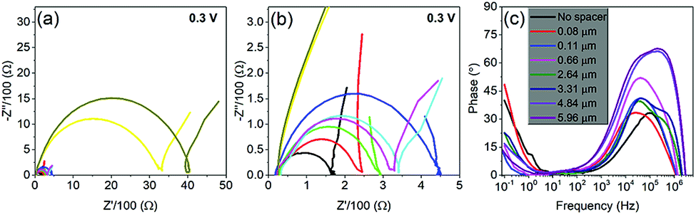 | ||
| Fig. 5 Nyquist plot (a and b) and Bode plot (c) of the FP-MPSC device with different spacer film thickness measured at 0.3 V, under weak illumination (0.1 sun). | ||
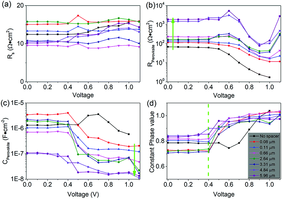 | ||
| Fig. 6 Parameters obtained from high frequency (∼102–106 Hz) semicircle IS analysis of the FP-MPSC device with different spacer film thickness measured at between 1.1 V and 0 V, under weak illumination (0.1 sun). (a) Series resistance. (b) Resistance related to perovskite. (c) Capacitance related to perovskite and (d) associated constant phase value. | ||
Combining the analysis about the effect of building block size and thickness of spacer layer, the bottlenecks of current spacer layer and infiltrated perovskite are summarized in left picture of Fig. 7. Perovskite layer embedded in mesoporous matrix of spacer layer are usually composed of crystals with size of tens of nanometers. Although observed quantum size effect may have useful application in LED or other optoelectronic fields, the limited charge transport ability in quantum dots is detrimental for achieving high PCE in photovoltaic device due to serious charge carrier recombination. Moreover, the thickness of spacer layer has to be several micrometers to insure enough insulating ability, which further hinders the charge transport to charge carrier selective layer. These two unfavorable factors decrease the potentially achievable PCE. It has been proved that grain boundaries are not beneficial for attaining high performance perovskite solar cells.1 Monolayer perovskite crystals in vertical direction are usually deposited on charge-selective layer in order to reduce recombination near grain boundary. According to the absorption coefficient of MAPbI3 perovskite, 1 μm thick MAPbI3 perovskite layer can absorb over 95% incident light at wavelength of 750 nm.15,33 Fixing the porosity of spacer layer to be 40%, 2.5 μm thick spacer layer has equivalent 1 μm thickness of perovskite layer. Considering that the size of perovskite crystals is less than 100 nm, the ratio of length of spacer thickness to size of perovskite crystals is over 25, which means that charge generated in spacer/perovskite layer has encountered at least 25 grain boundaries before reaching charge selective layer. To overcome these issues, the ideal features of spacer layer and infiltrated perovskite are illustrated in right picture of Fig. 7. Porous single-crystal perovskite models grown in matrix of porous spacer template with 2D arrays or 3D of structured films are more favorable for achieving high PCE.38 Perovskite nanorod has high mobility due to confined charge transport. It is known in the zeolite field that meso-crystal materials can grow from one ordered template, which needs controlled template–precursor interaction.39–41 In fact, porous single crystal MAPbI3 has been realized via additive in perovskite precursor solution.42 Some favorable phenomena has been also observed in investigating the crystallization of perovskite in mesopores of TSC films. For example, the crystal growth with preferential orientation was realized via moisture-induced crystallization process in the NH4Cl–PVSK complex.43 Even the perovskite crystal growth was significantly templated by scaffold, pronounced positive effect was occurred in photovoltaic performance. Therefore, exploring methods to grow mesoporous single-crystal perovskite with less grain boundaries and higher mobility in ordered spacer layer would further promote PCE of FP-MPSC device.
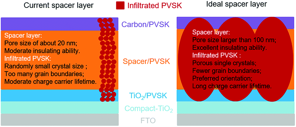 | ||
| Fig. 7 Illustration to show problems of current spacer layer and infiltrated perovskite, and proposed features of ideal spacer layer and infiltrated perovskite. | ||
Another issue to overcome is the unideal insulating ability of spacer film. The melting point of ZrO2 is about 2700 degrees. Sub-micrometer to nanometer ZrO2 is usually used to decrease the sintering temperature below 1000 degrees in the ceramic field.31 The particle size of ZrO2 has to be small enough to be sintered at allowed temperatures (the FTO glass will soften when T > 550 degrees).44 The insulating ability is mainly associated with porosity and interparticle connection. The porosity is similar for all particle size. The different insulating ability arises mainly from interparticle connection. To improve insulating ability, low-melting point wide bandgap nanomaterials is preferred as building blocks. Aluminum oxide, silica, or ternary oxides may provide better choice as spacer building blocks.45 Recently, by depositing a thin layer of Al2O3 onto surface of mesoporous TiO2 before printing spacer layer, the ZrO2 thickness was reduced from 3 μm to 1.2 μm while retaining comparable device performance.35
Conclusions
In this work, we have studied the effects of size of spacer building blocks, spacer thickness on optoelectronic property of perovskite, insulating property, and performance of FP-MPSC in details. The time-resolved PL and the band-edge emission spectrum of perovskite depends greatly on particle size of spacer building blocks. It was also found that the open-circuit voltage has clear relationship with insulating ability of spacer layer through varying spacer layer thickness in a large range. The charge transport feature in spacer layer is discussed with impedance spectra. Based on these deep understandings, it was proposed that advanced spacer film features pore size larger than 100 nm, high porosity and simultaneously ideal insulating ability with film thickness as thin as possible. Reasonable routes to realize ideal spacer layer are also proposed. The results will promote spacer improvement of FP-MPSC in the near future.Conflicts of interest
There are no conflicts to declare.Acknowledgements
The authors acknowledge the financial support of this work from the National Natural Science Foundation of China (Grant No. 51502141, 91733301, 91433203, 61474049, 51773230, and 21702069), the Ministry of Science and Technology of China (863, 2015AA034601), the Fundamental Research Funds for the Central Universities (No. 2019kfyXJJS051), the Program for HUST Academic Frontier Youth Team, the Science and Technology Department of Hubei Province (No. 2017AAA190), the 111 Project (No. B07038), the Double first-class research funding of China-EU Institute for Clean and Renewable Energy (No. ICARE-RP-2018-SOLAR-001 and ICARE-RP-2018-SOLAR-002), the Shenzhen Peacock Plan (KQTD2016053015544057), the Nanshan Pilot Plan (LHTD20170001), the NFSC/Hong Kong RGC Research Scheme (N_HKUST610/14), the Guangdong Science and Technology Program (2017B030314002), the HK-RGC General Research Funds (GRF No. 16312216), the HK Innovation and Technology Fund (ITS/219/16 and GHP/079/17SZ), and China Postdoctoral Science Foundation Grant (No. 2017M612452 and 2018M631240). We thank the Analytical and Testing Centre of Huazhong University of Science and Technology for field emission SEM testing.Notes and references
- C. Bi, Q. Wang, Y. Shao, Y. Yuan, Z. Xiao and J. Huang, Nat. Commun., 2015, 6, 7747 CrossRef CAS PubMed.
- Q. Dong, Y. Fang, Y. Shao, P. Mulligan, J. Qiu, L. Cao and J. Huang, Science, 2015, 347, 967–970 CrossRef CAS PubMed.
- F. Hao, C. C. Stoumpos, R. P. H. Chang and M. G. Kanatzidis, J. Am. Chem. Soc., 2014, 136, 8094–8099 CrossRef CAS PubMed.
- N. Kitazawa, Y. Watanabe and Y. Nakamura, J. Mater. Sci., 2002, 37, 3585–3587 CrossRef CAS.
- A. Kojima, K. Teshima, Y. Shirai and T. Miyasaka, J. Am. Chem. Soc., 2009, 131, 6050–6051 CrossRef CAS PubMed.
- H. Shi and M.-H. Du, Phys. Rev. B: Condens. Matter Mater. Phys., 2014, 90, 174103 CrossRef.
- W. J. Yin, T. Shi and Y. Yan, Adv. Mater., 2014, 26, 4653–4658 CrossRef CAS PubMed.
- W.-J. Yin, T. Shi and Y. Yan, Appl. Phys. Lett., 2014, 104, 063903 CrossRef.
- H. S. Kim, C. R. Lee, J. H. Im, K. B. Lee, T. Moehl, A. Marchioro, S. J. Moon, R. Humphry-Baker, J. H. Yum, J. E. Moser, M. Gratzel and N. G. Park, Sci. Rep., 2012, 2, 591 CrossRef PubMed.
- J. Burschka, N. Pellet, S.-J. Moon, R. Humphry-Baker, P. Gao, M. K. Nazeeruddin and M. Grätzel, Nature, 2013, 499, 316–319 CrossRef CAS PubMed.
- N. J. Jeon, J. H. Noh, Y. C. Kim, W. S. Yang, S. Ryu and S. I. Seok, Nat. Mater., 2014, 13, 897–903 CrossRef CAS PubMed.
- X. Li, M. I. Dar, C. Y. Yi, J. S. Luo, M. Tschumi, S. M. Zakeeruddin, M. K. Nazeeruddin, H. W. Han and M. Gratzel, Nat. Chem., 2015, 7, 703–711 CrossRef CAS PubMed.
- M. Liu, M. B. Johnston and H. J. Snaith, Nature, 2013, 501, 395–398 CrossRef CAS PubMed.
- W. Nie, H. Tsai, R. Asadpour, J. C. Blancon, A. J. Neukirch, G. Gupta, J. J. Crochet, M. Chhowalla, S. Tretiak, M. A. Alam, H. L. Wang and A. D. Mohite, Science, 2015, 347, 522–525 CrossRef CAS PubMed.
- Z. Xiao, Q. Dong, C. Bi, Y. Shao, Y. Yuan and J. Huang, Adv. Mater., 2014, 26, 6503–6509 CrossRef CAS PubMed.
- W. S. Yang, J. H. Noh, N. J. Jeon, Y. C. Kim, S. Ryu, J. Seo and S. I. Seok, Science, 2015, 348, 1234–1237 CrossRef CAS PubMed.
- Best Research-Cell Efficiencies, https://www.nrel.gov/pv/assets/pdfs/best-research-cell-efficiencies.20190802.pdf, 2019.
- Z. Ku, Y. Rong, M. Xu, T. Liu and H. Han, Sci. Rep., 2013, 3, 03132 CrossRef PubMed.
- L. F. Liu, A. Y. Mei, T. F. Liu, P. Jiang, Y. S. Sheng, L. J. Zhang and H. W. Han, J. Am. Chem. Soc., 2015, 137, 1790–1793 CrossRef CAS PubMed.
- T. Liu, L. Liu, M. Hu, Y. Yang, L. Zhang, A. Mei and H. Han, J. Power Sources, 2015, 293, 533–538 CrossRef CAS.
- A. Mei, X. Li, L. Liu, Z. Ku, T. Liu, Y. Rong, M. Xu, M. Hu, J. Chen, Y. Yang, M. Gratzel and H. Han, Science, 2014, 345, 295–298 CrossRef CAS PubMed.
- Z. Wei, K. Yan, H. Chen, Y. Yi, T. Zhang, X. Long, J. Li, L. Zhang, J. Wang and S. Yang, Energy Environ. Sci., 2014, 7, 3326–3333 RSC.
- K. Yan, Z. Wei, J. Li, H. Chen, Y. Yi, X. Zheng, X. Long, Z. Wang, J. Wang, J. Xu and S. Yang, Small, 2015, 11, 2269–2274 CrossRef CAS PubMed.
- X. Li, M. Tschumi, H. W. Han, S. S. Babkair, R. A. Alzubaydi, A. A. Ansari, S. S. Habib, M. K. Nazeeruddin, S. M. Zakeeruddin and M. Gratzel, Energy Technol., 2015, 3, 551–555 CrossRef CAS.
- Z. Meng, D. P. Guo, J. G. Yu and K. Fan, Appl. Surf. Sci., 2018, 430, 632–638 CrossRef CAS.
- H. Wang, G. Liu, X. Li, P. Xiang, Z. Ku, Y. Rong, M. Xu, L. Liu, M. Hu, Y. Yang and H. Han, Energy Environ. Sci., 2011, 4, 2025 RSC.
- T. Liu, Y. Rong, Y. Xiong, A. Mei, Y. Hu, Y. Sheng, P. Jiang, X. Hou, M. Duan, Y. Guan, L. Hong and H. Han, RSC Adv., 2017, 7, 10118–10123 RSC.
- E. A. Barringer and H. K. Bowen, J. Am. Ceram. Soc., 1982, 65, C-199–C-201 CrossRef CAS.
- C. T. Campbell, S. C. Parker and D. E. Starr, Science, 2002, 298, 811–814 CrossRef CAS PubMed.
- W. H. Rhodes, J. Am. Ceram. Soc., 1981, 64, 19–22 CrossRef CAS.
- I.-W. Chen and X.-H. Wang, Nature, 2000, 404, 168 CrossRef CAS PubMed.
- Y. Shao, Y. Yuan and J. Huang, Nat. Energy, 2016, 1, 1–6 Search PubMed.
- H. Chen, F. Ye, W. T. Tang, J. J. He, M. S. Yin, Y. B. Wang, F. X. Xie, E. B. Bi, X. D. Yang, M. Gratzel and L. Y. Han, Nature, 2017, 550, 92–95 CrossRef CAS PubMed.
- L. Ji, H. Y. Hsu, J. C. Lee, A. J. Bard and E. T. Yu, Nano Lett., 2018, 18, 994–1000 CrossRef CAS PubMed.
- Q. Wang, S. Liu, Y. Ming, Y. Guan, D. Li, C. Zhang, Z. Wang, Y. Rong, Y. Hu and H. Han, Sustainable Energy & Fuels, 2018, 2, 2412–2418 RSC.
- A. Dualeh, T. Moehl, N. Tetreault, J. Teuscher, P. Gao, M. K. Nazeeruddin and M. Gratzel, ACS Nano, 2014, 8, 4053 CrossRef CAS.
- A. Guerrero, G. Garcia-Belmonte, I. Mora-Sero, J. Bisquert, Y. S. Kang, T. J. Jacobsson, J.-P. Correa-Baena and A. Hagfeldt, J. Phys. Chem. C, 2016, 120, 8023–8032 CrossRef CAS.
- E. J. Crossland, N. Noel, V. Sivaram, T. Leijtens, J. A. Alexander-Webber and H. J. Snaith, Nature, 2013, 495, 215–219 CrossRef CAS PubMed.
- C. Dickinson, W. Zhou, R. P. Hodgkins, Y. Shi, D. Zhao and H. He, Chem. Mater., 2006, 18, 3088–3095 CrossRef CAS.
- K. Jiao, B. Zhang, B. Yue, Y. Ren, S. Liu, S. Yan, C. Dickinson, W. Zhou and H. He, Chem. Commun., 2005, 5618–5620 RSC.
- C. J. H. Jacobsen, C. Madsen, J. Houzvicka, I. Schmidt and A. Carlsson, J. Am. Chem. Soc., 2000, 122, 7116–7117 CrossRef CAS.
- T. Kollek, D. Gruber, J. Gehring, E. Zimmermann, L. Schmidt-Mende and S. Polarz, Angew. Chem., Int. Ed., 2015, 54, 1341–1346 CrossRef CAS PubMed.
- Y. Rong, X. Hou, Y. Hu, A. Mei, L. Liu, P. Wang and H. Han, Nat. Commun., 2017, 8, 14555 CrossRef PubMed.
- J.-C. Lee, T. G. Kim, W. Lee, S.-H. Han and Y.-M. Sung, Cryst. Growth Des., 2009, 9, 4519–4523 CrossRef CAS.
- Y. Xiong, X. Zhu, A. Mei, F. Qin, S. Liu, S. Zhang, Y. Jiang, Y. Zhou and H. Han, Sol. RRL, 2018, 2, 1800002 CrossRef.
Footnote |
| † Electronic supplementary information (ESI) available: Experimental section, Fig. S1–S5 and Table S1. See DOI: 10.1039/c9ra05357c |
| This journal is © The Royal Society of Chemistry 2019 |