
 Open Access Article
 This Open Access Article is licensed under a Creative Commons Attribution-Non Commercial 3.0 Unported Licence
High-performance and stable CsPbBr3 light-emitting diodes based on polymer additive treatment†
Wanqing Caia,
Ziming Chen*a,
Dongcheng Chena,
Shijian Su a,
Qinghua Xub,
Hin-Lap Yip*ac and
Yong Caoa
a,
Qinghua Xub,
Hin-Lap Yip*ac and
Yong Caoa
aState Key Laboratory of Luminescent Materials and Devices, Institute of Polymer Optoelectronic Materials and Devices, School of Materials Science and Engineering, South China University of Technology, 381 Wushan Road, Guangzhou, 510640, P. R. China. E-mail: mszimingchen@yahoo.com; msangusyip@scut.edu.cn
bDepartment of Chemistry, National University of Singapore, 117543 Singapore
cInnovation Center for Printed Photovoltaics, South China Institute of Collaborative Innovation, Dongguan 523808, P. R. China
First published on 3rd September 2019
Abstract
Because of their high efficiency and sharp emission, perovskite light-emitting diodes are a promising candidate for next-generation lighting techniques. However, the relatively poor stability of perovskite light-emitting diodes lowers their utility. Therefore, a highly stable perovskite light-emitting diode has to be developed to meet the commercial demand. Herein, we report a highly stable CsPbBr3 light-emitting diode via simple polymer treatment. The addition of 2-methyl-2-oxazoline in perovskite film assists the formation of CsPbBr3 nanocrystals, improving the quality and photoluminescence property of perovskite film. Based on such CsPbBr3 nanocrystals and polymer hybrid film, our device presents a high external quantum efficiency and luminance of around 3.0% and 16![[thin space (1/6-em)]](https://www.rsc.org/images/entities/char_2009.gif) 648 cd m−2, respectively. Moreover, an excellent device half-lifetime of more than 2.4 hours has been achieved, under continuous operation at a relatively high initial luminance of 1000 cd m−2, representing one of the most stable PeLEDs operated at such high initial luminance.
648 cd m−2, respectively. Moreover, an excellent device half-lifetime of more than 2.4 hours has been achieved, under continuous operation at a relatively high initial luminance of 1000 cd m−2, representing one of the most stable PeLEDs operated at such high initial luminance.
Introduction
In the past decade, metal halide perovskites have been widely investigated in optoelectronic applications such as solar cells, lasers and photodetectors.1–3 The impressive properties of metal halide perovskites, which include sharp emissions, tuneable bandgaps, low non-radiative recombination rates and balanced electron/hole mobility, also make them potential candidates for use in light-emitting diodes (LEDs).4–8 Since the pioneering report of perovskite LEDs (PeLEDs) based on organic–inorganic hybrid perovskites of CH3NH3PbBr3 in 2014, the external quantum efficiencies (EQE) of PeLEDs have constantly increased and currently exceed 20%.9–14Although the efficiency of PeLEDs developed very quickly, their inferior stability in devices has prevented the possibility of commercial application and hence lowered their overall utility. The instability of PeLEDs is mainly governed by the chemical and thermal instability of the emissive perovskite layer, particularly for organic–inorganic hybrid perovskite.15–18 For instance, reports show that MAPbBr3 (MA+ = CH3NH3+) suffers from thermal degradation even at temperatures below 100 °C.19–22 Also, increasing the annealing time of MAPbBr3 emission layers from 10 to 30 min (at 90 °C) causes sublimation of MABr and hence reduces its crystal quality, resulting in degraded performance of MAPbBr3-based PeLEDs.23 Therefore, it is crucial to develop emissive layers for LED application with better stability than organic–inorganic hybrid perovskites. Among the perovskite family, all-inorganic halide perovskites such as green-emissive CsPbBr3 have proven much more stable than organic–inorganic hybrid perovskite.24–32 For instance, the thermal-decomposition temperature of CsPbBr3 (580 °C) is much higher than that of MAPbBr3, which suggests that CsPbBr3 LEDs may possess superior thermal stability during long-term operation.33
In addition, as perovskite crystals in smaller size can provide a better confinement of injected charge carriers and hence display improved light-emitting properties, numerous investigations have studied PeLED based on perovskite nanocrystals.34–42 For example, it was found that the addition of a small amount of poly(ethylene oxide) to CsPbI3 system was an effective way to form α-phase small-grain CsPbI3 perovskite films at lower annealing temperatures.43 This insulating polymer could also passivate the pinholes and reduce the crystal size of CsPbBr3 films, leading to a PeLED with enhanced performance.38,44 Also, we have ever reported that introducing the polymer of poly(2-ethyl-2-oxazoline) into MAPbI3 and CsPbBrxI3−x systems can simultaneously reduce the crystal sizes and trap densities of perovskite films to produce near-infrared and pure-red PeLED with EQEs as high as 5.4% and 6.55%, respectively.25,45 Based on these previous reports, it is obvious that a suitable polymer additive can reduce the size of perovskite crystals and improve the overall performance of PeLEDs.
In this study, we combined stable all-inorganic perovskites with crystal size-reducing polymer additives to yield a highly stable CsPbBr3 LED with good device performance. We found that the addition of poly(2-methyl-2-oxazoline) (PMOXA) assisted the formation of both high-quality CsPbBr3 nanocrystals and a much stable perovskite phase. Meanwhile, PMOXA could passivate the surface traps of CsPbBr3 nanocrystals and consequently improve the overall photoluminescence quantum yield (PLQY) of the hybrid films. Using these high-quality CsPbBr3 nanocrystal films as an emissive layer, we successfully fabricated a green-emissive PeLED with maximum EQE and luminance of around 3.0% and 16648 cd m−2, respectively, and an excellent device half-lifetime of more than 2.4 hours under continuous operation at a relatively high initial luminance of 1000 cd m−2, representing one of the most stable PeLEDs operating at such high initial luminance. Moreover, the device presented an extremely narrow electroluminescence (EL) emission at 512 nm with a full width at half maximum (FWHM) of 18 nm and excellent spectrum stability, representing a high-quality green emission.
Results and discussion
As mentioned previously, the addition of polymer additives to perovskite film is a proven method to control perovskite crystal size and improve the resulting film quality.46–48 Inspired by these results, we added PMOXA to the CsPbBr3 precursor solutions to control the film morphology and crystal growth during the film formation process. We found that as the concentration of PMOXA in the precursor solution increased, the properties (absorption, photoluminescence [PL] emission, crystal quality and film morphology, etc.) of the resultant perovskite films changed accordingly.Fig. 1a shows that the absorption edge in pristine CsPbBr3 film is located at approximately 517 nm, but after the addition of PMOXA at concentrations from 5% to 25%, the absorption edge blue-shifted to approximately 512 nm. A similar phenomenon was also observed in the PL spectra (Fig. 1b), where the PL emission from pristine CsPbBr3 film was located at 517 nm, but after the addition of PMOXA at concentrations from 5% to 25%, the PL emission of perovskite film blue-shifted 5 nm to approximately 512 nm. We attributed the blue-shift of absorption and PL spectra after the incorporation of PMOXA to two possible reasons: the trap passivation effect from the PMOXA and the decrease of perovskite crystal sizes that could induce quantum confinement effects. Both aspects are discussed below.25,45
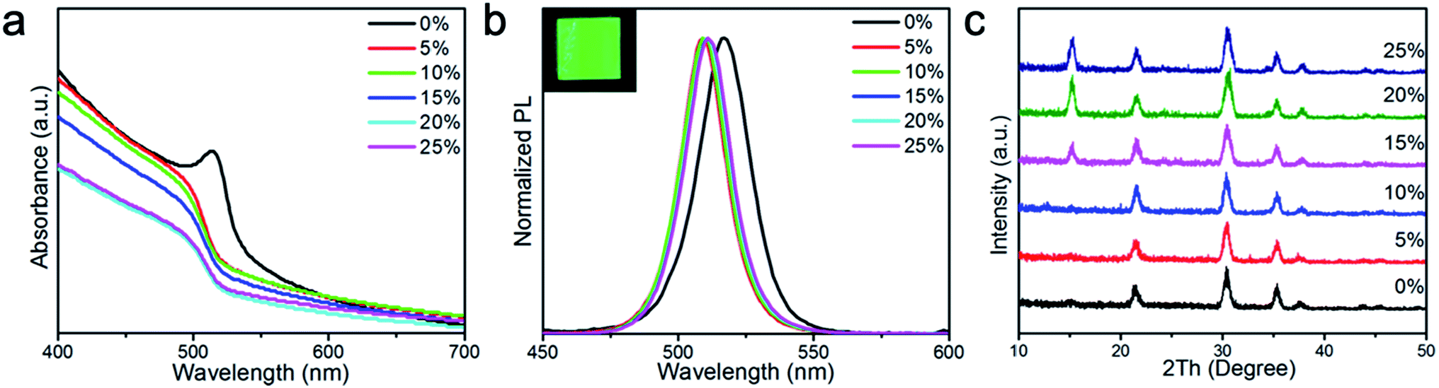 | ||
| Fig. 1 (a) Absorbances and (b) normalised PL spectra of CsPbBr3 films with various concentrations of PMOXA. The inserted image is the 20% PMOXA-treated CsPbBr3 film under UV lamp (365 nm) illumination. (c) XRD patterns of CsPbBr3 films with various concentrations of PMOXA. | ||
X-ray diffraction (XRD) patterns were measured to study the effect of the addition of PMOXA on the crystal structure of CsPbBr3, as shown in Fig. 1c. We observed diffraction peaks at 2θ of approximately 15.1°, 21.5°, 30.4° and 35.4° that could be assigned to the (100), (110), (200) and (210) planes of the cubic α-CsPbBr3 lattice, respectively. The peak positions were in complete correspondence with the diffraction patterns of the bulk materials obtained from the JCPDS database (no. 54-0752).49–51 We observed that the (100) peak appeared only when PMOXA was added in concentrations between 15% and 25%, suggesting that PMOXA could assist the formation of high-quality α-phase CsPbBr3 crystals and modulate their orientation.
Moreover, to understand the influence of PMOXA on the charge recombination properties within CsPbBr3 films, PL decay lifetimes were measured by time-correlated single photon counter, as shown in Fig. 2a. Bi-exponential decay functions (SE1) were fitted to the PL decay curves, where τ1 could be ascribed to the non-radiative recombination of initially photo-generated excitons through trap states, and τ2 corresponded to the bimolecularly radiative recombination of charge carriers. Accordingly, A1 and A2 were the fractions of the fast (τ1) and slow (τ2) decay components, respectively.52,53 The detailed values of τ1, τ2, A1, and A2 are summarised in Table S1.† We found that average PL lifetimes (τave) increased as the PMOXA concentration increased from 0% to 20% and decreased as the PMOXA concentration increased to 25%. The longest τave of 104.7 ns was obtained in 20% PMOXA-treated CsPbBr3 film, which is much longer than the τave in pristine CsPbBr3 film (36.1 ns). This result suggests that the addition of PMOXA could dramatically enhance the overall lifetime of photo-generated charge carriers, which would be beneficial to the relatively slow radiative recombination process. Moreover, it is apparent that A1 decreased significantly as the PMOXA concentrations increased from 0% to 20% and increased when the PMOXA concentration increased to 25%. Conversely, A2 increased significantly as the PMOXA concentrations increased from 0% to 20% and decreased when the PMOXA concentration increased to 25%. This result provides strong evidence that non-radiative recombination was significantly suppressed after the addition of PMOXA and therefore the portion of radiative recombination within the total recombination was enhanced.
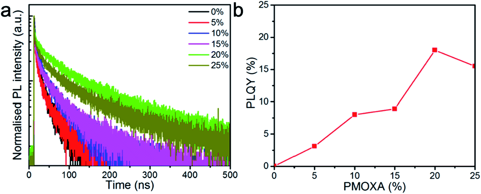 | ||
| Fig. 2 (a) PL lifetime traced at the emission peak of perovskite films with various concentrations of PMOXA under a fixed excitation fluence of 1 μJ cm−2 at the excitation wavelength of 365 nm. (b) PLQYs of CsPbBr3 films with various concentrations of PMOXA (excited at 1 mW cm−2). | ||
Furthermore, PLQYs of CsPbBr3 films with various concentrations of PMOXA were also investigated to confirm their PL properties. Fig. 2b shows that PLQY of CsPbBr3 film increased from 0.5% to 18% when PMOXA concentrations increased from 0% to 20%. Similarly, the PLQY dropped to 15.6% when too much PMOXA (25%) was added to this perovskite system. We attributed the improvement of PLQY after the incorporation of PMOXA to the suppression of non-radiative recombination, which was likely caused by the surface passivation effect from PMOXA, as the electron lone pair in the nitrogen and oxygen atom of PMOXA can coordinate with Pb2+ on the perovskite surface by Lewis base and Lewis acid interactions.54–58 However, the PL property dropped after the PMOXA concentration was increased to 25%; this could be attributed to the phase segregation of PMOXA and CsPbBr3 crystals and is discussed below.
Taken together, both the PL lifetime and PLQY results show that CsPbBr3 films with 20% PMOXA possessed the best PL properties and suggest that this case obtained the best potential for LED applications.
Aside from PL properties, film morphology is another critical factor that governs the final performance of PeLEDs. We therefore used scanning electron microscopy (SEM) and atomic force microscopy (AFM) to study the morphologies of CsPbBr3 films that contain various concentrations of PMOXA. As shown in Fig. 3 and S1,† the pristine CsPbBr3 film had poor film morphology, low film coverage and large film roughness (RMS = 6.9 nm), with crystal sizes of hundreds of nanometres; these properties are not suitable for LED application. After the introduction of PMOXA in concentrations of 5% to 25% into CsPbBr3 film, high-coverage films with reduced-size nanocrystals were successfully formed, resulting in a small film roughness of approximately 2 nm. However, with concentrations of PMOXA exceeding 25%, the perovskite crystals became large again, which may be attributable to phase segregation between the polymer phase and perovskite phase. Such phase segregation consequently enhanced the non-radiative recombination and thus reduced the PLQY of the perovskite film. We can expect that such a film is also not ideal for LED applications.
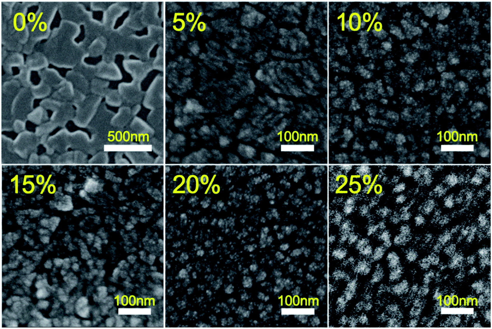 | ||
| Fig. 3 SEM images of CsPbBr3 films with various concentrations of PMOXA. | ||
The modulation of film morphology by PMOXA additives indicated that PMOXA may influence the formation process of CsPbBr3 crystals. To provide a deeper understanding of such effects, we performed transmission electron microscopy (TEM) to further characterise the crystal evolution in CsPbBr3 film treated with 20% PMOXA, before and after the annealing process (because the film with 20% PMOXA had the best potential for use in high-performance LED device). As shown in Fig. 4a, even before annealing, tiny crystals less than 10 nm in size had already been formed. We identified these as CsPbBr3 crystals based on the appearance of their (210) plane in the magnified image. After annealing, these crystals grew to bigger CsPbBr3 perovskite nanocrystals of tens of nanometres in size, as shown in Fig. 4b. The magnified image shows a (100) plane of CsPbBr3 nanocrystal with a complete lattice, which illustrates that these nanocrystals were in high quality.59,60
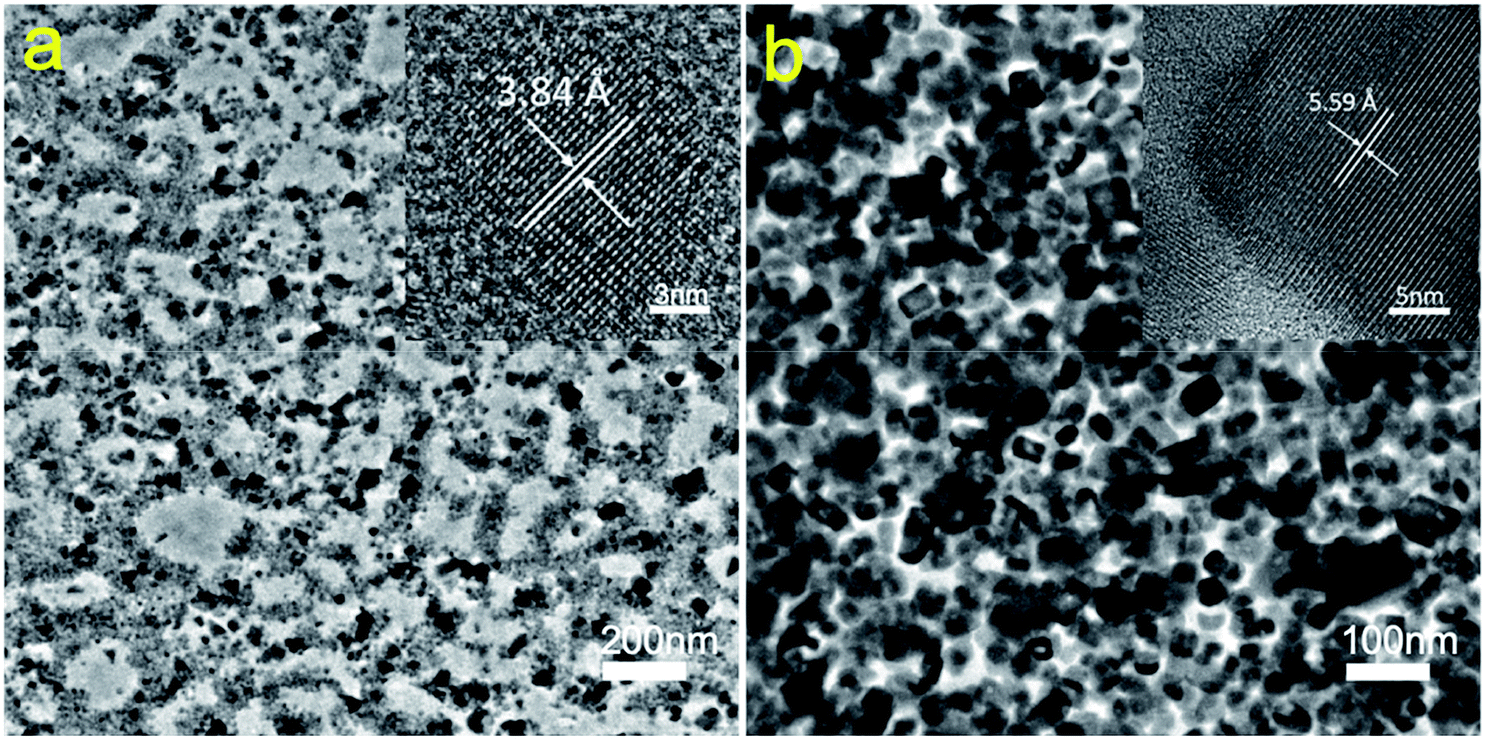 | ||
| Fig. 4 (a) TEM image of 20% PMOXA-treated CsPbBr3 film without annealing. Scale bar: 200 nm. Inset image is the high-resolution TEM image of crystal. Scale bar: 3 nm. (b) TEM image of 20% treated-PMOXA CsPbBr3 film with annealing. Scale bar: 100 nm. Inset image is the high-resolution TEM image of crystal. Scale bar: 5 nm. | ||
According to previous reports that the electron lone pair in C![[double bond, length as m-dash]](https://www.rsc.org/images/entities/char_e001.gif) O can coordinate with Pb2+ in perovskite and thus influence the nucleation and growth process of perovskite crystals,20,38 we therefore also consider that CO in PMOXA could strongly coordinate with Pb2+ in PbBr2, facilitating the formation of tiny CsPbBr3 crystals in spin-coated films and that such tiny crystals also act as sites of nucleation. During the annealing process, the dissociated CsBr and PbBr2 can interact with such nucleation sites, resulting in the further growth of CsPbBr3 nanocrystals. Meanwhile, the limited space in the polymer matrix restricted the further growth of CsPbBr3 nanocrystals to less than 100 nm.
O can coordinate with Pb2+ in perovskite and thus influence the nucleation and growth process of perovskite crystals,20,38 we therefore also consider that CO in PMOXA could strongly coordinate with Pb2+ in PbBr2, facilitating the formation of tiny CsPbBr3 crystals in spin-coated films and that such tiny crystals also act as sites of nucleation. During the annealing process, the dissociated CsBr and PbBr2 can interact with such nucleation sites, resulting in the further growth of CsPbBr3 nanocrystals. Meanwhile, the limited space in the polymer matrix restricted the further growth of CsPbBr3 nanocrystals to less than 100 nm.
To evaluate the EL properties of CsPbBr3/PMOXA hybrid films, perovskite LEDs with a device structure of indium oxide (ITO)/PEDOT:PSS/perovskite/TPBi/LiF/Al were fabricated (Fig. 5a), where PEDOT:PSS and TPBi acted as the hole and electron transport layers, respectively. Fig. 5b shows the energy level of each functional layer. Such device architecture presented a proper energy-level alignment of both electron and hole injection to the light-emitting layer. The performances of CsPbBr3 LEDs with various concentrations of PMOXA are summarised in Table 1 and in Fig. 6a and b.
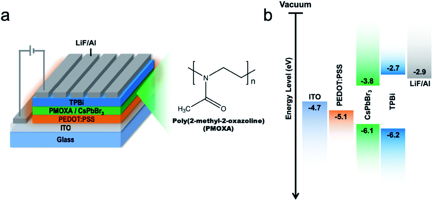 | ||
| Fig. 5 (a) Schematic device structure. (b) Energy diagram of each layer of the LED device. The energy level of CsPbBr3 are cited from ref. 61. | ||
| PMOXA ratio | Von (V) | Lmax (cd m−2) | CEmax (cd A−1) | EQEmax (%) | CIE (x,y) |
|---|---|---|---|---|---|
| 10% | 3.1 | 11452 |
5.4 | 1.8 | (0.06,0.74) |
| 15% | 3.0 | 13772 |
6.8 | 2.2 | (0.07,0.75) |
| 20% | 3.0 | 16648 |
10.1 | 3.0 | (0.08,0.77) |
| 25% | 3.1 | 2693 | 7.8 | 2.2 | (0.09,0.78) |
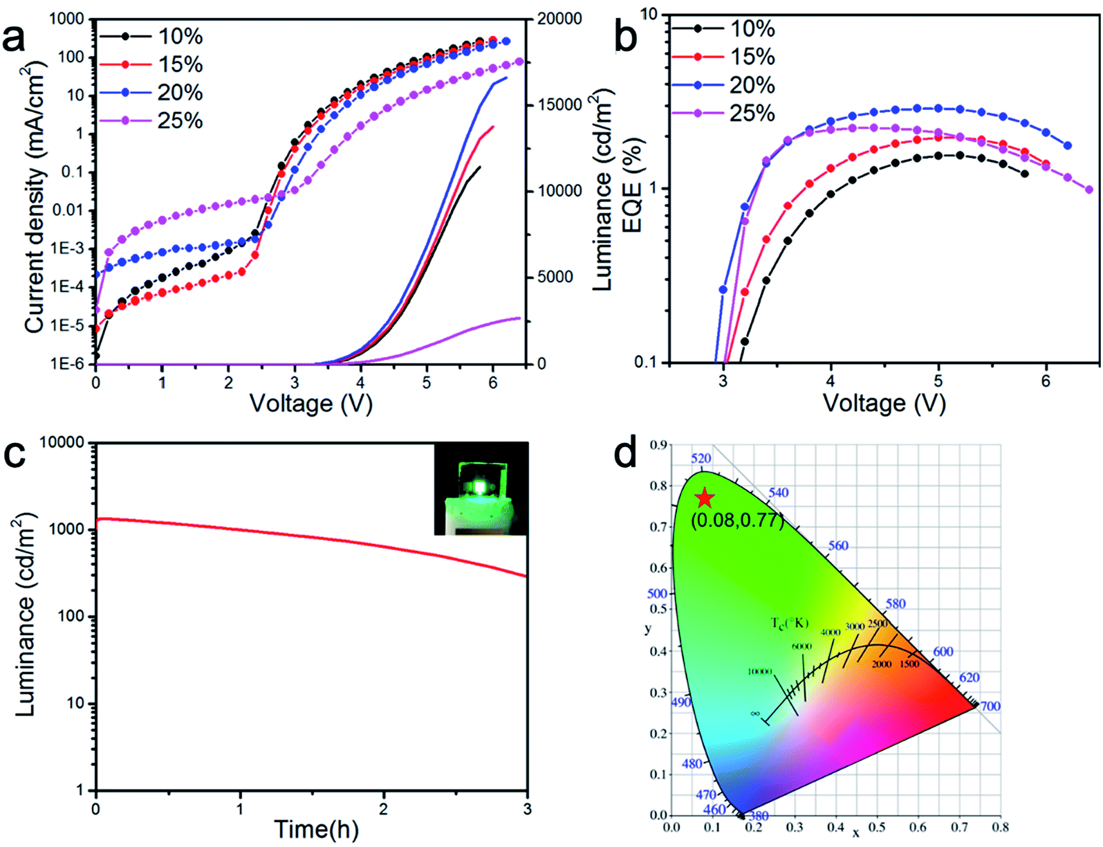 | ||
| Fig. 6 (a) Current density and luminance versus voltage characteristics of CsPbBr3 LEDs with various concentrations of PMOXA. Solid lines and dotted lines correspond to luminance and current density, respectively. (b) EQE versus voltage characteristic of CsPbBr3 LEDs with various concentrations of PMOXA. (c) Stability measurement of CsPbBr3 LED with 20% PMOXA. Initial luminance was 1000 cd m−2. The inserted image is the photo of such LED illuminated at 1000 cd m−2. (d) CIE coordinate of CsPbBr3 LED with 20% PMOXA. | ||
No EL was obtained for films of 0% and 5% PMOXA-treated CsPbBr3, because of their poor PL properties, crystal qualities and film morphologies. However, when the concentration of PMOXA was increased from 10% to 20%, the device performance improved rapidly. The highest luminance, EQE and current efficiency of 16648 cd m−2, 3.0% and 10.1 cd A−1, respectively, were achieved at relatively low applied voltage in the device containing 20% PMOXA-treated CsPbBr3. Further increasing the concentration of PMOXA to 25% resulted in a decrease in device performance. These device performance-changes can be explained by the aforementioned observations: that the film quality and PLQY was improved when we increased the PMOXA concentration from 0% to 20%, whereas poorer film quality and PLQY resulted if we further increased the PMOXA concentration to 25%.
The EL emission peak of the 20% PMOXA-treated CsPbBr3 device was located at 512 nm with a narrow FWHM of 18 nm, which corresponded to Commission International de 1′Eclairage (CIE) colour coordinates of (0.08, 0.77) (Fig. 6d). As shown in Fig. S2,† the EL spectra showed no change at a different applied current density, which suggests that such a device displayed excellent spectral stability. In addition, when the device was operated at a high initial luminance of 1000 cd m−2, a 2.4 hour half-lifetime could be obtained (as shown in Fig. 6c), which represents one of the best results for green-emissive PeLEDs at such a high initial luminance (Table S2†).
In summary, we have demonstrated a simple approach to form high-quality CsPbBr3 perovskite films by treatment with polymer additives. The addition of PMOXA can modify the morphology of perovskite film, reduce the crystal size, passivate crystal surface-traps and improve the PLQY of perovskite film. Also, such polymer additives may coordinate with Pb2+, which could control the nucleation and growth process of perovskite, resulting in the in situ growth of CsPbBr3 nanocrystals. In the optimised conditions of CsPbBr3 film treated with 20% PMOXA, a highly efficient perovskite LED was fabricated with a maximum EQE of 3.0% and luminance of 16648 cd m−2. The LED also showed a low turn-on voltage of 3.0 V and CIE of (0.08, 0.77), which are properties of an excellent green-emissive LED. More importantly, the LED fabricated from 20% PMOXA-treated CsPbBr3 presented excellent spectrum stability and a half-lifetime of 2.4 hour under an initial luminance of 1000 cd m−2, highlighting the potential of 20% PMOXA-treated CsPbBr3-based LEDs for future applications, such as white-light illuminations and full-colour displays.
Experimental section
All chemicals were used as received without further purification.Perovskite precursor
0.2 mmol PbBr2 and 0.36 mmol CsBr were dissolved in 1 mL DMSO to form a 0.2 M perovskite precursor solution. Appropriate amounts of PMOXA (Sigma-Aldrich) were dissolved in the resulting CsPbBr3 solutions. The relative weight ratio of x% PMOXA means mPMOXA/mCsPbBr3 = x%. The precursor solution was stirred overnight at room temperature.Film characterisation
Ultraviolet-visible light absorptions were measured with HP8453 spectrophotometer. The PL spectra were measured with a spectrofluorometer (PerkinElmer LS 55).AFM (Digital Instrumental [DI] Multimode Nanoscope IIIa) and SEM (ZEISS Merlin) measurements were carried out based on the structure of ITO/PEDOT/perovskite. TEM samples were prepared according to the structure of ITO/PMMA/PEDOT:PSS/perovskite. The PMMA film was dissolved in chlorobenzene, and the PEDOT:PSS/perovskite film could be separated from the substrate, which was suitable for TEM measurement. The TEM samples were measured by JEM-2100F. XRD measurement was carried out based on the structure of ITO/PEDOT/perovskite by an X-ray diffractometer (PANalytical X'pertPRO) equipped with Cu-Kα X-ray tube.
PLQY and PL lifetime measurement
PLQY values were obtained from perovskite films on glass at the excitation wavelength of 365 nm using a calibrated integrating sphere. Time-resolved PL lifetime measurements were performed with a transient photoluminescence spectrometer (FLS980, Edinburgh Instruments) equipped with a time-correlated single-photon counting unit. A picosecond laser diode (405 nm, pulse width = 50 ps) was used as the excitation source.Perovskite LED device fabrication
ITO-coated glass substrates were cleaned successively by sonication in detergent, acetone, deionised water and isopropyl alcohol. After 4 min of oxygen plasma treatment, diluted PEDOT:PSS (Clevios, 4083) was spin-coated on ITO-coated glass substrate at 3000 rpm for 30 s and then annealed at 150 °C for 15 min in a laboratory atmosphere; 0.2 M perovskite precursor solution was then spin-coated on PEDOT:PSS film at 3500 rpm for 30 s and annealed for 20 min in a glovebox at 130 °C. A 50 nm-thick TPBi was evaporated onto the perovskite layer, followed by the deposition of LiF (1 nm) and Al (120 nm) by thermal deposition in a vacuum chamber (pressure ≈ 2 × 10⁻⁶ Torr). The device's active area was 0.1 cm2.Perovskite LED device characterisation
Current density–voltage–radiance measurement was carried out with a Keithley 2400 source measurement unit and a Konica Minolta Chroma Meter CS-200. The electroluminescence spectra and CIE coordinates were recorded with an Ocean Optics USB 2000+ spectrometer. The external quantum efficiency values were calculated assuming a Lambertian emission profile. All the perovskite LEDs were measured in air after encapsulation.Author contributions
Cai W. fabricated the perovskite LEDs and carried out the device characterizations. Cai W., Chen Z., and Chen D. carried out the perovskite film characterizations. Chen Z. and Cai W. analyzed the data and wrote the manuscript. Chen Z. and Yip H.-L. led the project. Yip H.-L., Su S., Xu Q. and Cao Y. supervised the research.Conflicts of interest
The authors declare that they have no conflict of interest.Acknowledgements
This study was financially supported by the Ministry of Science and Technology of the People's Republic of China (No. 2017YFA0206600), the National Natural Science Foundation of China (No. 21761132001, 51573057 and 91733302) and China Postdoctoral Science Foundation (No. 2019M650197).References
- Z. Wang, Q. Lin, B. Wenger, M. G. Christoforo, Y.-H. Lin, M. T. Klug, M. B. Johnston, L. M. Herz and H. J. Snaith, Nat. Energy, 2018, 3, 855–861 CrossRef CAS.
- Z. Yang, Y. Deng, X. Zhang, S. Wang, H. Chen, S. Yang, J. Khurgin, N. X. Fang, X. Zhang and R. Ma, Adv. Mater., 2018, 30, 1704333 CrossRef PubMed.
- T. J. S. Evans, A. Schlaus, Y. Fu, X. Zhong, T. L. Atallah, M. S. Spencer, L. E. Brus, S. Jin and X. Y. Zhu, Adv. Opt. Mater., 2018, 6, 1700982 CrossRef.
- L. Protesescu, S. Yakunin, M. I. Bodnarchuk, F. Krieg, R. Caputo, C. H. Hendon, R. X. Yang, A. Walsh and M. V. Kovalenko, Nano Lett., 2015, 15, 3692–3696 CrossRef CAS PubMed.
- Z. Chen, C. Zhang, X. F. Jiang, M. Liu, R. Xia, T. Shi, D. Chen, Q. Xue, Y. J. Zhao, S. Su, H. L. Yip and Y. Cao, Adv. Mater., 2017, 29, 1603157 CrossRef PubMed.
- Z. Xiao, R. A. Kerner, L. Zhao, N. L. Tran, K. M. Lee, T.-W. Koh, G. D. Scholes and B. P. Rand, Nat. Photonics, 2017, 11, 108–115 CrossRef CAS.
- X. Li, Y. Wu, S. Zhang, B. Cai, Y. Gu, J. Song and H. Zeng, Adv. Funct. Mater., 2016, 26, 2435–2445 CrossRef CAS.
- G. R. Yettapu, D. Talukdar, S. Sarkar, A. Swarnkar, A. Nag, P. Ghosh and P. Mandal, Nano Lett., 2016, 16, 4838–4848 CrossRef CAS PubMed.
- Y. Cao, N. Wang, H. Tian, J. Guo, Y. Wei, H. Chen, Y. Miao, W. Zou, K. Pan, Y. He, H. Cao, Y. Ke, M. Xu, Y. Wang, M. Yang, K. Du, Z. Fu, D. Kong, D. Dai, Y. Jin, G. Li, H. Li, Q. Peng, J. Wang and W. Huang, Nature, 2018, 562, 249–253 Search PubMed.
- T. Chiba, Y. Hayashi, H. Ebe, K. Hoshi, J. Sato, S. Sato, Y.-J. Pu, S. Ohisa and J. Kido, Nat. Photonics, 2018, 12, 681–687 CAS.
- K. Lin, J. Xing, L. N. Quan, F. P. G. de Arquer, X. Gong, J. Lu, L. Xie, W. Zhao, D. Zhang, C. Yan, W. Li, X. Liu, Y. Lu, J. Kirman, E. H. Sargent, Q. Xiong and Z. Wei, Nature, 2018, 562, 245–248 CAS.
- H. Cho, S.-H. Jeong, M.-H. Park, Y.-H. Kim, C. Wolf, C.-L. Lee, J. H. Heo, A. Sadhanala, N. Myoung, S. Yoo, S. H. Im, R. H. Friend and T.-W. Lee, Science, 2015, 350, 1222–1225 CrossRef CAS PubMed.
- X. Yang, X. Zhang, J. Deng, Z. Chu, Q. Jiang, J. Meng, P. Wang, L. Zhang, Z. Yin and J. You, Nat. Commun., 2018, 9, 570–578 CrossRef PubMed.
- N. Wang, L. Cheng, R. Ge, S. Zhang, Y. Miao, W. Zou, C. Yi, Y. Sun, Y. Cao, R. Yang, Y. Wei, Q. Guo, Y. Ke, M. Yu, Y. Jin, Y. Liu, Q. Ding, D. Di, L. Yang, G. Xing, H. Tian, C. Jin, F. Gao, R. H. Friend, J. Wang and W. Huang, Nat. Photonics, 2016, 10, 699–704 CrossRef CAS.
- X. Zhao and N.-G. Park, Photonics, 2015, 2, 1139–1151 CrossRef CAS.
- Y. H. Kim, H. Cho, J. H. Heo, T. S. Kim, N. Myoung, C. L. Lee, S. H. Im and T. W. Lee, Adv. Mater., 2015, 27, 1248–1254 CrossRef CAS PubMed.
- Y.-H. Kim, C. Wolf, Y.-T. Kim, H. Cho, W. Kwon, S. Do, A. Sadhanala, C. G. Park, S.-W. Rhee, S. H. Im, R. H. Friend and T.-W. Lee, ACS Nano, 2017, 11, 6586–6593 CrossRef CAS PubMed.
- J.-W. Lee, Y. J. Choi, J.-M. Yang, S. Ham, S. K. Jeon, J. Y. Lee, Y.-H. Song, E. K. Ji, D.-H. Yoon, S. Seo, H. Shin, G. S. Han, H. S. Jung, D. Kim and N.-G. Park, ACS Nano, 2017, 11, 3311–3319 CrossRef CAS PubMed.
- L. Dimesso, C. Wittich, T. Mayer and W. Jaegermann, J. Mater. Sci., 2019, 54, 2001–2015 CrossRef CAS.
- Z. Song, N. Shrestha, S. C. Watthage, G. K. Liyanage, Z. S. Almutawah, R. H. Ahangharnejhad, A. B. Phillips, R. J. Ellingson and M. J. Heben, J. Phys. Chem. Lett., 2018, 9, 6312–6320 CrossRef CAS PubMed.
- R. K. Misra, S. Aharon, B. Li, D. Mogilyansky, I. Visoly-Fisher, L. Etgar and E. A. Katz, J. Phys. Chem. Lett., 2015, 6, 326–330 CAS.
- R. K. Singh, R. Kumar, A. Kumar, N. Jain, R. K. Singh and J. Singh, J. Alloys Compd., 2018, 743, 728–736 CrossRef CAS.
- Y.-H. Kim, H. Cho, J. H. Heo, S. H. Im and T.-W. Lee, Curr. Appl. Phys., 2016, 16, 1069–1074 CrossRef.
- J. Pan, Y. Shang, J. Yin, M. De Bastiani, W. Peng, I. Dursun, L. Sinatra, A. M. El-Zohry, M. N. Hedhili, A. H. Emwas, O. F. Mohammed, Z. Ning and O. M. Bakr, J. Am. Chem. Soc., 2018, 140, 562–565 CrossRef CAS PubMed.
- W. Cai, Z. Chen, Z. Li, L. Yan, D. Zhang, L. Liu, Q.-h. Xu, Y. Ma, F. Huang, H.-L. Yip and Y. Cao, ACS Appl. Mater. Interfaces, 2018, 10, 42564–42572 CrossRef CAS PubMed.
- Y. Tian, C. Zhou, M. Worku, X. Wang, Y. Ling, H. Gao, Y. Zhou, Y. Miao, J. Guan and B. Ma, Adv. Mater., 2018, 30, e1707093 CrossRef PubMed.
- J. Song, J. Li, X. Li, L. Xu, Y. Dong and H. Zeng, Adv. Mater., 2015, 27, 7162–7167 CrossRef CAS.
- L. Zhang, X. Yang, Q. Jiang, P. Wang, Z. Yin, X. Zhang, H. Tan, Y. M. Yang, M. Wei, B. R. Sutherland, E. H. Sargent and J. You, Nat. Commun., 2017, 8, 15640 CrossRef CAS.
- Y. Shang, G. Li, W. Liu and Z. Ning, Adv. Funct. Mater., 2018, 28, 1801193 CrossRef.
- J. Li, L. Xu, T. Wang, J. Song, J. Chen, J. Xue, Y. Dong, B. Cai, Q. Shan, B. Han and H. Zeng, Adv. Mater., 2017, 29, 1603885 CrossRef PubMed.
- J. Xing, Y. Zhao, M. Askerka, L. N. Quan, X. Gong, W. Zhao, J. Zhao, H. Tan, G. Long, L. Gao, Z. Yang, O. Voznyy, J. Tang, Z. H. Lu, Q. Xiong and E. H. Sargent, Nat. Commun., 2018, 9, 3541 CrossRef PubMed.
- M. K. Gangishetty, S. Hou, Q. Quan and D. N. Congreve, Adv. Mater., 2018, 30, e1706226 CrossRef PubMed.
- M. Yuan, L. N. Quan, R. Comin, G. Walters, R. Sabatini, O. Voznyy, S. Hoogland, Y. Zhao, E. M. Beauregard, P. Kanjanaboos, Z. Lu, D. H. Kim and E. H. Sargent, Nat. Nanotechnol., 2016, 11, 872–877 CrossRef CAS PubMed.
- G. Li, F. W. Rivarola, N. J. Davis, S. Bai, T. C. Jellicoe, F. de la Pena, S. Hou, C. Ducati, F. Gao, R. H. Friend, N. C. Greenham and Z. K. Tan, Adv. Mater., 2016, 28, 3528–3534 CAS.
- J. Li, X. Shan, S. G. Bade, T. Geske, Q. Jiang, X. Yang and Z. Yu, J. Phys. Chem. Lett., 2016, 4059–4066 Search PubMed.
- H. Cho, C. Wolf, J. S. Kim, H. J. Yun, J. S. Bae, H. Kim, J. M. Heo, S. Ahn and T. W. Lee, Adv. Mater., 2017, 29, 1700579 CrossRef PubMed.
- J. Shamsi, P. Rastogi, V. Caligiuri, A. L. Abdelhady, D. Spirito, L. Manna and R. Krahne, ACS Nano, 2017, 11, 10206–10213 CAS.
- C. Wu, Y. Zou, T. Wu, M. Ban, V. Pecunia, Y. Han, Q. Liu, T. Song, S. Duhm and B. Sun, Adv. Funct. Mater., 2017, 27, 1700338 CrossRef.
- J. Pan, Y. Shang, J. Yin, M. De Bastiani, W. Peng, I. Dursun, L. Sinatra, A. M. El-Zohry, M. N. Hedhili, A. H. Emwas, O. F. Mohammed, Z. Ning and O. M. Bakr, J. Am. Chem. Soc., 2018, 140, 562–565 CrossRef CAS PubMed.
- M. Imran, V. Caligiuri, M. Wang, L. Goldoni, M. Prato, R. Krahne, L. De Trizio and L. Manna, J. Am. Chem. Soc., 2018, 140, 2656–2664 CrossRef CAS PubMed.
- D. K. Sharma, S. Hirata, V. Biju and M. Vacha, ACS Nano, 2019, 13, 624–632 CrossRef CAS PubMed.
- Y. Shen, L. P. Cheng, Y. Q. Li, W. Li, J. D. Chen, S. T. Lee and J. X. Tang, Adv. Mater., 2019, e1901517 CrossRef PubMed.
- B. Jeong, H. Han, Y. J. Choi, S. H. Cho, E. H. Kim, S. W. Lee, J. S. Kim, C. Park, D. Kim and C. Park, Adv. Funct. Mater., 2018, 28, 1706401 CrossRef.
- J. Li, X. Shan, S. G. Bade, T. Geske, Q. Jiang, X. Yang and Z. Yu, J. Phys. Chem. Lett., 2016, 4059–4066 CrossRef PubMed.
- Z. Chen, Z. Li, C. Zhang, X. F. Jiang, D. Chen, Q. Xue, M. Liu, S. Su, H. L. Yip and Y. Cao, Adv. Mater., 2018, 30, e1801370 CrossRef PubMed.
- G. Li, Z. K. Tan, D. Di, M. L. Lai, L. Jiang, J. H. Lim, R. H. Friend and N. C. Greenham, Nano Lett., 2015, 15, 2640–2644 CrossRef CAS PubMed.
- Y. Ling, Y. Tian, X. Wang, J. C. Wang, J. M. Knox, F. Perez-Orive, Y. Du, L. Tan, K. Hanson, B. Ma and H. Gao, Adv. Mater., 2016, 28, 8983–8989 CrossRef CAS PubMed.
- J. Li, S. G. Bade, X. Shan and Z. Yu, Adv. Mater., 2015, 27, 5196–5202 CrossRef CAS PubMed.
- R. J. Sutton, G. E. Eperon, L. Miranda, E. S. Parrott, B. A. Kamino, J. B. Patel, M. T. Hörantner, M. B. Johnston, A. A. Haghighirad, D. T. Moore and H. J. Snaith, Adv. Energy Mater., 2016, 6, 1502458 CrossRef.
- X. Chang, W. Li, L. Zhu, H. Liu, H. Geng, S. Xiang, J. Liu and H. Chen, ACS Appl. Mater. Interfaces, 2016, 8, 33649–33655 CrossRef CAS PubMed.
- T. Burwig, W. Fränzel and P. Pistor, J. Phys. Chem. Lett., 2018, 9, 4808–4813 CrossRef CAS PubMed.
- Z. Shi, S. Li, Y. Li, H. Ji, X. Li, D. Wu, T. Xu, Y. Chen, Y. Tian, Y. Zhang, C. Shan and G. Du, ACS Nano, 2018, 12, 1462–1472 CrossRef CAS PubMed.
- H. Cho, J. S. Kim, C. Wolf, Y. H. Kim, H. J. Yun, S. H. Jeong, A. Sadhanala, V. Venugopalan, J. W. Choi, C. L. Lee, R. H. Friend and T. W. Lee, ACS Nano, 2018, 12, 2883–2892 CrossRef CAS PubMed.
- L. Song, X. Guo, Y. Hu, Y. Lv, J. Lin, Z. Liu, Y. Fan and X. Liu, J. Phys. Chem. Lett., 2017, 8, 4148–4154 CrossRef CAS PubMed.
- N. Wang, L. Cheng, J. Si, X. Liang, Y. Jin, J. Wang and W. Huang, Appl. Phys. Lett., 2016, 108, 141102 CrossRef.
- N. Ahn, D. Y. Son, I. H. Jang, S. M. Kang, M. Choi and N. G. Park, J. Am. Chem. Soc., 2015, 137, 8696–8699 CrossRef CAS PubMed.
- X. Cao, C. Li, Y. Li, F. Fang, X. Cui, Y. Yao and J. Wei, Nanoscale, 2016, 8, 19804–19810 RSC.
- Y. Jo, K. S. Oh, M. Kim, K.-H. Kim, H. Lee, C.-W. Lee and D. S. Kim, Adv. Mater. Interfaces, 2016, 3, 1500768 CrossRef.
- J. Zhang, L. Fan, J. Li, X. Liu, R. Wang, L. Wang and G. Tu, Nano Res., 2019, 12, 121–127 CrossRef CAS.
- J. Zhang, L. Zhang, P. Cai, X. Xue, M. Wang, J. Zhang and G. Tu, Nano Energy, 2019, 62, 434–441 CrossRef CAS.
- Y. Tan, Y. Zou, L. Wu, Q. Huang, D. Yang, M. Chen, M. Ban, C. Wu, T. Wu, S. Bai, T. Song, Q. Zhang and B. Sun, ACS Appl. Mater. Interfaces, 2018, 10, 3784–3792 CrossRef CAS PubMed.
Footnote |
| † Electronic supplementary information (ESI) available. See DOI: 10.1039/c9ra05270d |
| This journal is © The Royal Society of Chemistry 2019 |