DOI:
10.1039/C9RA04750F
(Paper)
RSC Adv., 2019,
9, 33207-33221
Unraveling the effect of Gd doping on the structural, optical, and magnetic properties of ZnO based diluted magnetic semiconductor nanorods†
Received
24th June 2019
, Accepted 11th October 2019
First published on 16th October 2019
Abstract
The structural, magnetic, and optical properties of the pristine and Gd-doped ZnO nanorods (NRs), prepared by facile thermal decomposition, have been studied using a combination of experimental and density functional theory (DFT) with Hubbard U correction approaches. The XRD patterns demonstrate the single-phase wurtzite structure of the pristine and doped ZnO. The rod-like shape of the nanoparticles has been examined by FESEM and TEM techniques. Elemental compositions of the pure and doped samples were identified by EDX measurement. Due to the Burstein–Moss shift, the optical band gaps of the doped samples have been widened compared to pristine ZnO. The PL spectra show the presence of complex defects. Room temperature magnetic properties have been measured using VSM and revealed the coexistence of paramagnetic and weak ferromagnetic ordering in Gd3+ doped ZnO-NRs. The magnetic moment was increased upon addition of more Gd ions into the ZnO host lattice. The DFT+U calculations confirm that the presence of vacancy-complexes has a significant effect on the structural, electronic, and magnetic properties of a pristine ZnO system.
1. Introduction
Synthesis of semiconductor materials with unique magnetic, photocatalytic and optical properties appear to be the upcoming candidates for the next generation of spintronics, electronic, and optoelectronic devices.1 Owing to their technological importance, the wide band gap semiconductors, such as ZnO,2 GaN,3 AlN,4 and InN5 have attracted more consideration among other semiconductors. Particularly, zinc oxide (ZnO) has been studied extensively, thanks to its large exciton binding energy (60 meV),6 outstanding chemical and thermal stabilities,7 and wide-direct bandgap (3.37 eV).8 Thus, many academics have investigated its practical applications in solar cells,9 optoelectronics devices,10 sensors,11 field emission devices,12 transparent electrodes,13 and spintronics devices.14 The electronic and magnetic properties of the low-dimension materials with defect-free lattice structure are exceptional, but structural defects, either made deliberately or unintentionally, play a key role in redecorating their properties.15,16 Hence, the existence of various types of cation or anion vacancies and interstitials in ZnO nanocrystals may alter their magnetic, photocatalytic and photoluminescence performances.17
Among the wide band gap semiconductors, ZnO possesses the richest morphologies. Many types of one-dimensional (1D) ZnO nanocrystals, like nanowires,18 nanotubes,19 nanorods,20 and nanobelts,21 have been grown. In general, several synthesis methods have been established to grow 1D ZnO nanostructures, such as electrochemical deposition,22 thermal evaporation,23 the template method,24 chemical vapor deposition (CVD),20 hydrothermal process,25 and the sol–gel method.26 However, these approaches require a rigorous control synthesis environment, expensive equipment, and complicated procedures. Our study reports facile synthesis route of Gd3+ doped ZnO-NRs and the study of its essential properties. To the knowledge of the authors, only a few scholars27–29 have reported the preparation of rod-like shape Zn1−xGdxO (x = 0.03 and 0.06).
ZnO can be diluted with a vast number of ions to meet the demand of various applications area. The diluted magnetic semiconductors (DMSs), wherein the spin degree of freedom is introduced to charge, show remarkable features such as magnetic, magneto-electronic, and magneto-optoelectronic, caused by the mutual impact of magnetic and semiconducting demeanor.30,31 ZnO doped with 3d transition metals (TMs) ions have been extensively investigated in several experimental32–34 and theoretical35,36 studies. In comparison with TMs, 4f rare earth (RE) constituents have greater magnetic moments and expected to enhance the ferromagnetism in DMSs.37 Especially, Gd3+ doped ZnO nanomaterials are the most debatable. Although some experimental and DFT results confirmed the existence of room temperature ferromagnetism (RTFM)38–40 property in Gd3+ doped wurtzite ZnO, there are numbers of studies have established the absence of RTFM.41,42 In addition to magnetic properties, one more attractive feature of the 4f ions doped ZnO nanocrystals is their optical response. Several experimental and theoretical investigations have reported that RE-doped ZnO can absorb ultraviolet (UV) light.43–45 Furthermore, the calculations based on DFT have delivered extensive understanding into the properties of three-dimensional and two-dimensional materials.46–52
In the present paper, Zn1−xGdxO (x = 0, 0.03 and 0.06) nanorods have been synthesized by thermal decomposition of zinc acetate dehydrate and gadolinium acetate hydrate as main precursors. The prepared powders were examined by means of several characterization techniques, like X-ray diffraction (XRD), transmission electron microscopy (TEM), field-emission scanning electron microscopy (FE-SEM), energy dispersive X-ray spectroscopy (EDX), vibrating sample magnetometer (VSM), photoluminescence and ultraviolet-visible (UV-vis) spectroscopy. Furthermore, DFT+U calculations were employed to understand the effect of the impurities on the electronic and magnetic properties of ZnO crystal at the atomic scale.
2. Experimental procedure
2.1. Materials
Analytical grade of zinc acetate dihydrate Zn(CHOO)2·2H2O and gadolinium acetate hydrate Gd(CHOO)2·H2O were used to prepare pristine and doped ZnO-NRs.
2.2. Synthesis procedure
Zn(CHOO)2·2H2O was used as a precursor for synthesizing pristine ZnO nanorods.32 A specific amount of the precursor was ground in a mortar and pestle for 1 h and placed in a crucible. The crucible was heated to 400 °C in an air atmosphere with a heating rate of 80 °C per hour and held for 1 h, producing ZnO-NRs in powder form.
Gadolinium-doped zinc oxide (Zn1−xGdxO) nanorods, where x = 3.0 and 6.0 atomic percent, were prepared by the same procedure described above from zinc and gadolinium acetates. Note that the atomic weight ratios of Zn(CHOO)2·2H2O and Gd(CHOO)2·H2O were maintained to obtain stoichiometric amounts of zinc-gadolinium oxide (Zn1−xGdxO).
3. Theoretical modelling
The theoretical results have been achieved utilizing the pseudopotential method based on density functional theory as implemented in CASTEP code.53 Ultrasoft pseudopotential method54 along with energy cut-off of 500 eV was used for geometry optimization. A supercell contains 16 atoms of Zn and 16 atoms of O has been created to model the effect of impurities on the electronic properties of ZnO crystal. In order to model Gd3+ impurities in ZnO, one atom of Zn2+ was substituted by Gd3+ atom which represents the chemical formula Zn15GdO16. This gives a Gd3+ concentration of 6.25 percent. Further, the effect of cation vacancy (Zn15GdO16 + VZn) and anion vacancy (Zn15GdO16 + VO) complexes has also been studied. Spin-polarized generalized gradient approximation (GGA+U), where U is the Hubbard parameter due to the Coulomb repulsion, was used to understand the precise behavior of electronic band structure and magnetic properties of the pristine and doped systems. The on-site Coulomb interaction U equals to (UZn-d) 10 eV,55 (UO-p) 7 eV (ref. 35) and (UGd-f) 6 eV (ref. 56) was employed to define the correlation influence in the localized of d, p and f orbitals of Zn, O and Gd, respectively. Our main goal is to widen the calculated band gap of ZnO to experimental value by introducing UO-p parameter.57 The Brillouin zone integration was performed in the Monkhorst–Pack scheme utilizing 5 × 5 × 4 k-points. The benchmarks of convergence for atomic force and energy were set to be 0.001 Å and 10−5 eV, respectively. We achieved self-consistency with the convergence tolerance set to 10−6 eV per atom. The valence states for Zn, Gd, and O atoms were selected to be 3d104s2, 4f75s25p65d16s2, and 2s22p4, respectively.
4. Results and discussion
4.1. Structural and microstructure analysis
The XRD patterns of the pristine and Gd3+ doped ZnO nanostructures are depicted in Fig. 1. All the diffraction peaks were characteristic for the hexagonal wurtzite structure of ZnO (ICDD #01-074-0534, ICSD #26170) and have space group P63mc with lattice parameters a = 3.245 Å and c = 5.207 Å, see ESI Fig. S1(a).† No impurity peaks were observed, such as Gd cluster or Gd2O3, indicating that the gadolinium quantity is less than the solubility limits.58 However, we cannot exclude the probability of the development of clusters or precipitates of secondary amorphous phase small enough not to be identified by the XRD measurements. The intensity of the XRD lines was augmented as the doping concentration increased and the FWHM became broader than that of the pristine ZnO-NRs. This can point out that the doped specimens possessed higher crystallinity with small coherent domain size and large strain triggered by crystal defects compared to the pristine ZnO-NRs. The diffraction peak of 6% Gd-doped ZnO (2θ = 34.305°) has shifted towards lower angles compared to the pristine ZnO-NRs (2θ = 34.355°) as shown in the inset of Fig. 1. This is due to the fact the ionic radii of Gd3+ (0. 93 Å) is larger than that of Zn (0.74 Å).59 This trend is consistent with the previous experimental reports.59,60 Peak shifting may indicate that the crystallographic positions of Zn2+ ions have been successfully occupied by Gd3+ ions in the ZnO host lattice and strain developed in the lattice61 (see-Fig. S1(b)).†
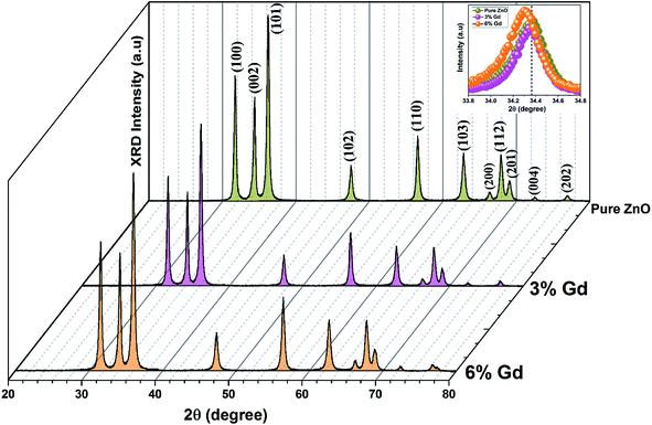 |
| | Fig. 1 X-ray diffraction patterns of pristine and Gd-doped ZnO-NRs annealed at 400 °C for 1 h. The X-ray diffractograms show that the prepared samples are polycrystalline with hexagonal wurtzite phase. The inset shows the shift of the diffraction peak along (002) plane at varying doping concentrations. | |
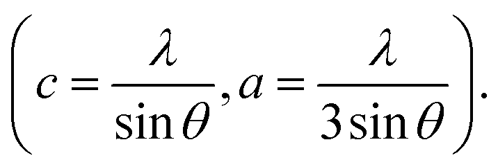
To better understand the impact of Gd3+ ions on the structural parameters of pristine ZnO-NRs, Rietveld refinement has been used. Rietveld-refined XRD patterns of the pristine and doped ZnO-NRs are given in Fig. 2(a). The pseudo-Voigt function was utilized to describe the XRD line profiles. Firstly, we check the quality parameters of the refined patterns, such as goodness of fit (GOF), weighted residual parameter (Rwp), Bragg factor (RB), and expected residual parameter (Rexp). The values of these parameters listed in Table S1† indicate that derived samples are of high quality and refinements are effective. Observed and calculated values were good matching as can be recognized from figures and are consistent with previous studies.62,63 Then, the lattice constants (a, c), c/a ratio, degree of distortion (R), unit cell volume (V), and bond length (along c-axis) have been calculated systematically using Rietveld refinement implemented in X'pert highscore plus software. The obtained data are plotted in Fig. 3 and tabulated in Table S2.† One may suppose the expansion of lattice parameters (a, c) as a result of peak shifting in the direction of lower 2θ angles  64 In our refined XRD patterns, the lattice parameters (a, c and V) show a reverse trend where both a and c lattice constants were decreased upon Gd addition (Fig. 3(a) and (b)). This may be attributed to several factors, such as the concentration of dopant, defects (vacancies, interstitial, dislocation), external strains developed due to temperature, and the difference between the ionic radii of Gd and Zn ions.65,66 A similar trend has been found for RE-doped ZnO nanoparticles.64,65,67,68 The a, c lattice parameters and the unit cell volumes (V) progressively decrease as Gd doping concentration increases to 0.03 and, then, a becomes constant while c and V values slightly increase with the increment of the doping concentration. The probable clarification of the perceived trend is that for low concentration of Gd3+, the lattice contraction occurs up to a critical concentration caused by the hydrostatic pressure produced by the rare earth dopants located on the surface of the ZnO-NRs. Upon additional increase in dopant concentration, the crystal lattice expands owing to the substitution of Zn atoms in the core due to relatively large ionic radii of Gd3+ ion. The contraction trends of c parameter upon Gd doping has also been reported by Flemban et al.56 and e Silva et al.69 The substitution of Zn2+ in the tetrahedral site of the ZnO host lattice by Gd3+ ions will cause lattice distortion. The perfect wurtzite structure has a hexagonal unit cell with two lattice constants, a and c, with a ratio of c/a = 1.633.70 Deviation of the crystal from the perfect arrangement can be measured in expressions of the degree of distortion
  (thus, R = 1 represents no distortion).71 As shown in Fig. 3(c), the c/a ratio and R values were deviated from the ideal value as doping concentration increase, indicating the presence of lattice distortion (anion or cation vacancies).72 Variations of bond lengths with Gd-concentration are illustrated in Fig. 3(d). The variation of bond lengths develops the lattice strain.34 The substitution of Gd atoms in Zn sites attracts oxygen atoms closer, causing elongation of Zn–O bond lengths along c-axis whereas Zn–Zn bond length decreases significantly and then becomes constant at higher doping concentration. Although Zn–O bond length expands along c-axis, it contracts along the a–b axis upon doping (not shown here). We also perceived that the interplanar spacing (d) slightly increased from 2.6028 to 2.6119 Å with an increase of Gd3+ content. This can be attributed to the higher electronegativity of Zn2+ (1.65) compared to that of Gd3+ (1.2), which leads to decrease the attraction force between Gd3+ and O2− than the force between Zn2+ and O2−. Moreover, we have also performed possible non-stoichiometry of anion and cation in the ZnO of both the pristine ZnO-NRs and possible dopant (Gd) concentration at the Zn sites of ZnO host lattice.73 This can be understood from the “Site Occupancy Factor (SOF)” column of Table S1, Fig. S2(a) and (b).† The related discussion of the SOF refinement for prepared products was described in the ESI.†
 |
| | Fig. 2 (a) Rietveld refinement analysis and (b) Williamson–Hall plot of pure and doped ZnO nanoparticles. The CIF file contained the necessary parameters of the crystal structure of ZnO (ICSD #26170) was achieved from ICSD database implemented in findit software to simulate the observed XRD patterns using Rietveld refinement. | |
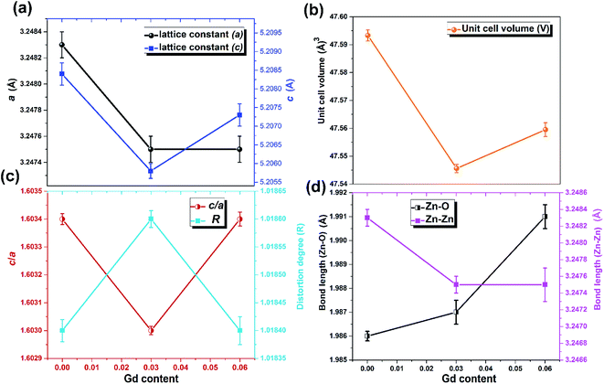 |
| | Fig. 3 Variation of (a) lattice parameters a and c, (b) unit cell volume, (c) c/a ratio and distortion degree, and (d) bond lengths Zn–O and Zn–Zn with Gd content. | |
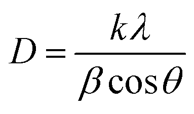
The average coherent domain size was estimated from the full width at half maximum (FWHM) of the strongest three diffraction peaks (100), (002), and (101) using the Scherrer equation.31
| |
 | (1) |
Along with the coherent domain size, lattice strain also donates to the broadening of the XRD peaks and has been assessed utilizing the Williamson–Hall (W–H) plot based on the following formula.64
| |
 | (2) |
where
θ is the diffraction angle,
β is the FWHM of the diffraction peak,
k is the geometric parameter (0.9),
λ is the wavelength of X-ray used (
λ = 1.5406 Å),
D is the domain size, and
ε is the effective strain. The strain was predicted from the slope, and the domain size (
D) was estimated from the intercept of a plot of
β![[thin space (1/6-em)]](https://www.rsc.org/images/entities/char_2009.gif)
cos
θ against sin
θ as shown in
Fig. 2(b). For a precise examination of the size and strain effects, the instrumental peak profile must be considered. The diffraction pattern from the line broadening of a standard material
viz., high crystalline silicon powder was measured to deconvolute the aforementioned influences and to determine the instrumental profile using the following expressions.
| | |
βstrain = [βobs2 − βstd2]1/2
| (4) |
where
βstd,
βobs, and
β describe the silicon, ZnO, and corrected structural broadening, respectively. By using the Scherrer formula, the average domain size of pristine ZnO-NRs was estimated to be 23.23 nm. The incorporation of 6% Gd into the ZnO-NRs causes a decrease in the average coherent domain size down to 19.7 nm as shown in Table S2.
† Fig. 2(b) shows the plot of
βcos
θ versus sin
θ for pristine ZnO-NRs (applying
eqn (2)) and the slope value is +0.0009. The positive slope value indicates the tensile strain. It is evident from the scattered data in
Fig. 2(b) that the data do not entirely obey the W–H formulation for different samples where they show a non-monotonous increase of
βcos
θ versus sin
θ. This indicates that the broadening of Bragg peaks with respect to different Bragg reflections are anisotropic and caused by anisotropic microstrain. The microstrain anisotropy observed in these nanorods is ascribed to the presence of point defects.
74,75 Similar behavior has been found for ZnO nanorods by Khanchandani
et al.76 The obtained coherent domain size is 29.8 nm for pristine ZnO-NRs, while it equals to 28.9 for 6% Gd-doped sample. For all samples, one may perceive that the coherent domain sizes measured by W–H plot are greater than those calculated by Scherrer routine since the latter does not reflect the impact of lattice defects on the XRD peaks broadening. For 6% Gd-doped sample, the strain has been increased to +0.001, indicating the presence of higher lattice defects compared to the pristine structure. The obtained results are in line with previous experimental reports.
58,60,65,77 The reduction in the coherent domain size is mainly attributed to the distortion in the ZnO structure by the incorporation Gd
3+ ions which decrease the nucleation and subsequent growth rate of ZnO-NRs. Besides, the dislocation density (
δ) was estimated employing the formula below,
78 where
D is the coherent domain size. This provides more understanding of the concentration of defects in the nanostructures.
| |
 | (5) |
The calculated values of the dislocation density are given in Table S2.† It is obvious that the dislocation density increased with increasing Gd content in the ZnO host lattice and the results are consistent with the previous calculations.60,79
4.2. Morphological and EDX characterization
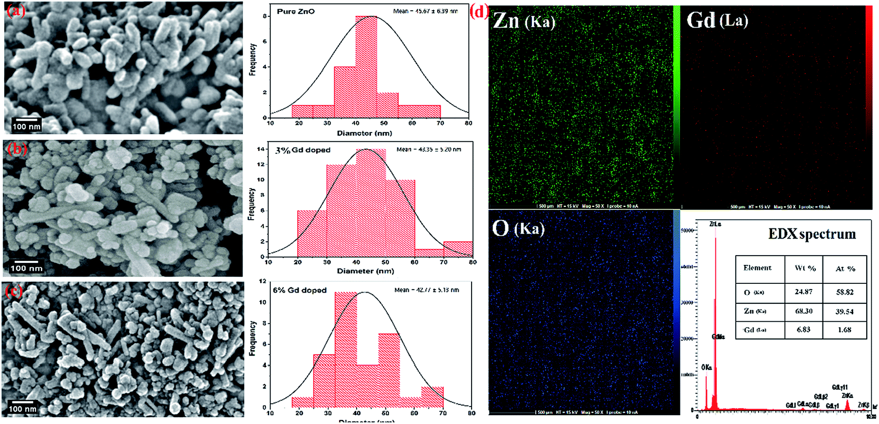
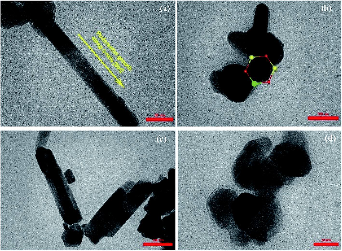
The morphology of the synthesized products has been studied by means of field emission electron microscopy scanning (FESEM) and transmission electron microscopy (TEM) as shown in Fig. 4 and 5, respectively. The overall reaction and grain growth mechanism of ZnO nanoparticles throughout the thermal decomposition of zinc acetate have been described in details elsewhere.32,80 FESEM images show that the pristine and doped ZnO has a rod-like shape morphology. It is evidently noticeable from Fig. 4 (b) and (c) that Gd3+ doping decreases the size of ZnO nanostructures, in case of pristine ZnO (Fig. 4(a)) there is rod-like morphology with a mean diameter of ∼45 nm ± 6 nm, and with 3% and 6% Gd3+ doping the diameters change to ∼43 nm ± 5 nm, and ∼42 nm ± 5 nm, respectively (see-Fig. 4 particle size distribution). Note that the coherent domain size from XRD line profiles was smaller than the particle size achieved from FESEM analysis. This may be as a result of the agglomeration of lots of small domains to form a particle. The mean length of pure and doped rods was found to be ∼161 nm ± 4 nm, ∼248 nm ± 6 nm, and ∼297 nm ± 7 nm, respectively. The calculated average aspect ratios of the pure and doped ZnO-NRs are close to the value of the standard aspect ratio of nanorods (3–5). It is evident that Gd doping enhances the aspect ratio of ZnO nanorods. So as to ratify the purity of the prepared ZnO-NRs and incorporation of Gd ions in ZnO-NRs, the EDX spectrum was recorded from the pure and doped sample, see Fig. S3† and 4(e), respectively. The absence of any extra emission demonstrates the quality and purity of the prepared product, see Fig. S3.† In general, ZnO is an n-type semiconductor where most defects are zinc interstitials (Zni) and VO.81 In contrast, we achieve deficiency of zinc and excess of oxygen atoms in the prepared ZnO nanorods. Consequently, the excess of oxygen, may be ascribed to the presence VZn or Oi in ZnO nanoparticles.82 The excessive oxygen may give rise to less observed experimental p-type semiconducting behavior in the prepared ZnO-NRs as shown Fig. S3.† Furthermore, the EDX mapping of 3% Gd-doped ZnO-NRs was collected from the selected area of the typical electron image as shown in Fig. 4(e). Panels in Fig. 4(e) demonstrate the elemental mapping of Zn, Gd, and O respectively, which show the existence of Gd in ZnO-NRs. The actual doping of 3% Gd in the ZnO-NRs was assessed from EDX in terms of atomic and weight percentage (see-the table inset in Fig. 4(e)). The EDX results demonstrate that the chemical composition varies slightly with rich oxygen content, and almost close to the nominal composition. TEM images of 3% and 6% Gd3+ doped ZnO sample confirm that the ZnO particles are grown in the shape of a rod as presented in Fig. 5. Fig. 5(a–c) represents the preferential growth of ZnO-NRs along c-axis, whereas Fig. 5(b–d) illustrates the rod-like shape of the doped samples.
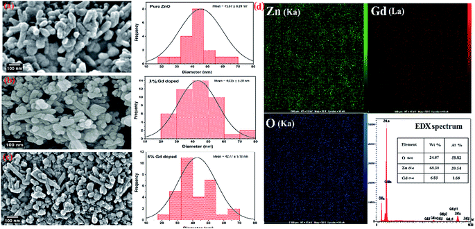 |
| | Fig. 4 FESEM images of (a) pristine ZnO, (b) 3% Gd-doped ZnO, (c) 6% Gd-doped ZnO along with their particle size distribution histogram and (d) EDX elemental mapping of 3% Gd-doped ZnO. The inset table shows the quantitutive results of doped samples. | |
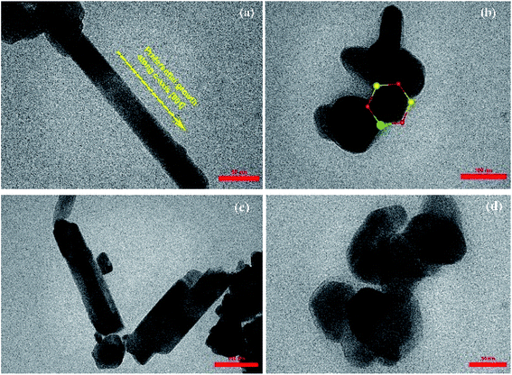 |
| | Fig. 5 TEM images of (a and b) 3% Gd-doped ZnO and its hexagonal shape and (c and d) 6% Gd-doped ZnO with its hexagonal shape. | |
4.3. Optical properties
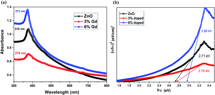
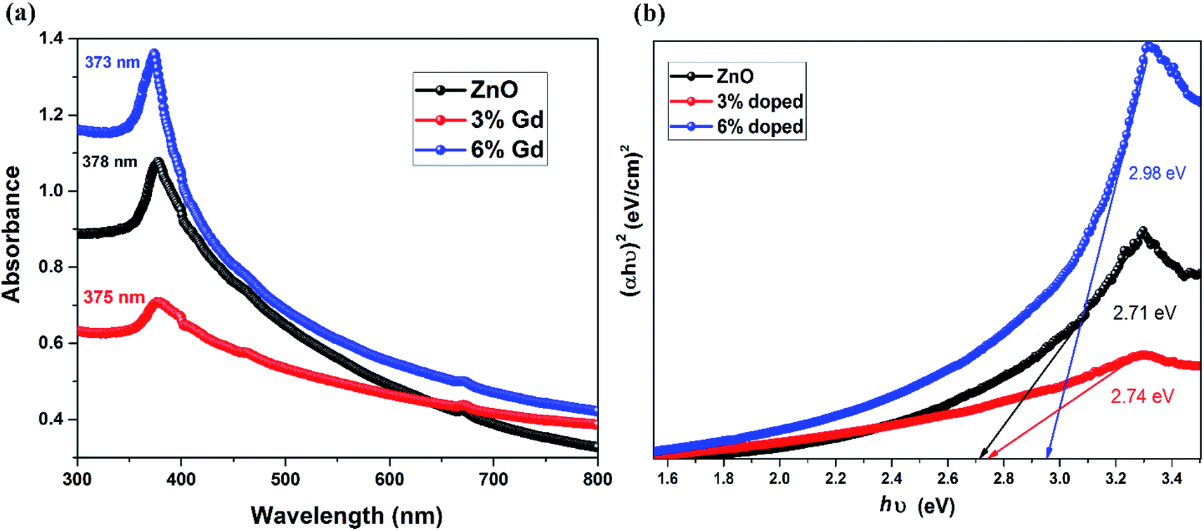
The UV-vis spectra of pristine and Gd-doped ZnO-NRs are demonstrated in Fig. 6. The prepared nanorods were dispersed in ethanol prior to measuring the optical absorption spectra in the wavelength ranging from 300 to 800 nm at a step of 1 nm. The spectra were rectified to the solvent absorption contribution. The optical absorption spectra of all three samples display a robust absorption around 370–480 eV, and the peaks have been slightly shifted toward shorter wavelength values (blue shift) upon Gd doping in ZnO-NRs as shown in Fig. 6(a). Note that 6% Gd doping enhances the absorbance intensity of pristine ZnO-NRs in the UV region, which is ascribed to the doping induced increase in the electron concentration.83 The absorption peak centered at 378 nm is the characteristic peak for hexagonal wurtzite ZnO nanoparticles.84 The pristine ZnO-NRs show blue-shifted absorption peak with regard to their bulk counterpart having the absorption peak at 386 nm.85 Several methods have been suggested to determine the band gap energy (E) from optical absorption measurements.86 In this study, the direct band gaps of pristine and doped ZnO-NRS were calculated using the Tauc's plot as given below:where α is the absorption coefficient, C is constant, h is Planck's constant, ν is the photon frequency, and Eg is the optical band gap. For a direct transition, n = 1/2. An extrapolation of the linear region of a plot of (αhν)2 on the Y-axis versus the photon energy hν on the X-axis gives the value of the Eg, see Fig. 6(b). It was observed that the calculated band gap of pristine ZnO, 3% Gd-doped ZnO, and 6% Gd-doped ZnO are 2.71, 2.74, and 2.98 eV, respectively. The band gap of pristine zinc oxide decreases compared to the defect-free ZnO (3.37 eV)8 due to the increase in point defects (cation or anion vacancies) that are generated during the thermal decomposition process. On the other hand, the band gap of pristine ZnO-NRs increases upon doping. A similar kind of phenomenon has been reported by Mithal et al.67 and Mazhdi et al.87
 |
| | Fig. 6 (a) UV-visible spectra of the ZnO and Gd-doped ZnO nanorods and (b) Tauc's plot of the ZnO and Gd-doped ZnO nanorods. | |
It has been reported that particle size reduction leads to widening the bandgap of metal oxides due to quantum confinement effect.88 In this letter, the particle size reduction has been confirmed by XRD and FESEM analysis. Since the dimensions of the prepared nanostructures are larger than the exciton Bohr radius of ZnO (2.38 nm), the size effect is implausible to cause the perceived blue shift. Furthermore, this blue shift in bandgap can be ascribed to the Burstein–Moss phenomena89 where the change in bandgap is directly proportional to the carrier concentration. Therefore, the augment in the carrier concentration with Gd ions in ZnO will cause Fermi level to move into the conduction band. In this case, the optical transition of electrons takes place from the valance band to the energy levels in the conduction band, which is positioned above the Fermi level. This effect the shifting of self-absorption peak at higher energy, and consequently the optical gap will be equivalent to E (actual band-gap) + dE (Moss–Burstein effect). These results support our assumption that the Gd cations have successfully decorated the wurtzite structure of ZnO and substituted the Zn cations sites.
4.4. Photoluminescence analysis
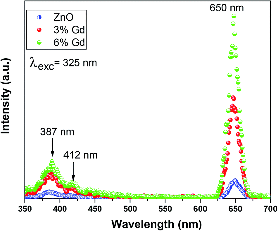
Photoluminescence (PL) measurement is a sensitive non-destructive method to study the extrinsic and intrinsic defects in semiconductors. It offers important information on the energy levels of these defects, even at low densities, which is useful for understanding the structural defects in semiconductors.90 The room temperature PL spectra of pure and doped ZnO-NRs using 325 nm wavelength light source are illustrated in Fig. 7. It is noticeable that the pristine ZnO has three distinct emission bands, (i) low intense peak at 387 nm corresponding to UV emission, (ii) low intense peak centered at 412 nm corresponding to violet emission, (iii) high intense and sharp peaks centered at 650 nm signifies the orange-red emission.
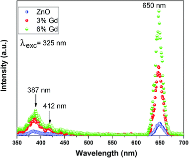 |
| | Fig. 7 Photoluminescence spectra of pure ZnO and ZnO:Gd (3% and 6%). | |
The UV emission band can be described by a near band-edge (NBE) transition that is responsible for the recombination of free ZnO excitons.87 The intensity of UV emission has been enhanced as the concentration of Gd ions increase. This is because Gd doping increases the crystalline quality of ZnO-NRs, hence augments the density of free exciton. The obtained results are in good agreement with previous experimental report.28 Substitution of divalent Zn2+ ions with trivalent Gd3+ ions results in crystalline defects in ZnO, such as zinc interstitials (Zni), zinc vacancies (VZn), oxygen interstitials (Oi) and oxygen vacancies (VO). The violet emission at 412 nm is accredited to the transition from conductive band to zinc vacancy (VZn),91 which has been increased upon Gd doping. The orange-red PL band was earlier attributed either to oxygen interstitial atoms (Oi) due to excess oxygen on the ZnO surface or to the hydroxyl group (OH).92 The orange emission is caused by transition from the Zn interstitial (Zni) to the oxygen interstitial (Oi) states. Such phenomena are generally observed in oxygen rich systems, see the results of EDX. Other reports show that VZn-related acceptor defects were assumed to be responsible for the deep-level emission near 650 nm.93 This type of emission is still controversial. Based on the obtained results, complex defects can be existed in the prepared nanoparticles, especially Gd–VZn defects.
4.5. Magnetic properties
To study the magnetic behaviors of Gd3+ doped ZnO-NRs, magnetization hysteresis loops were conducted using VSM at room temperature. Fig. 8 shows the magnetizations versus applied magnetic field (M–H) loops for pure and doped ZnO-NRs. The data show the existence of two components, one is weak ferromagnetism and the other is a dominant paramagnetic ordering at room temperature. The presence of weak ferromagnetic ordering in pure ZnO can be ascribed to VZn.94 Furthermore, a similar co-existence of ferromagnetic and paramagnetic orderings has been observed in ZnO doped with other RE metal ions such as Er95 and Tb.96 The narrow opening and S-shape hysteresis loops with a saturation field in order of 500 Oe are due to the weak ferromagnetism of the doped samples, see inset of Fig. 8. Coercive field (HC) and remanent magnetization (Mr) values of the M versus H curve have trivial magnitudes. The coercive field (HC), measured by means of HC = (HC+ − HC−/2), where HC+ and HC− are the values on the positive and negative H field sides when M = 0, respectively, and remanent magnetization (Mr) values, at 300 K are 56 Oe and 0.7 memu g−1 in the 3% Gd-doped ZnO-NRs, and 26 Oe and 1 memu g−1 in the 6% Gd-doped ZnO-NRs. This observation is consistent with the previous experimental reports.58,60,77 Interestingly, we have also observed that the magnetic moment of the 6% Gd-doped ZnO-NRs (0.26 emu g−1) is twice larger than that of the 3% Gd-doped sample (0.13 emu g−1) which indicates more dopant (Gd) incorporation in 6% doped sample. This is consistent with our expectation since more Gd ions substitutions should result in more magnetic moment. Therefore, the magnetization rises with increasing Gd-concentration and room temperature ferromagnetism augments progressively. Thus, Gd basically plays a significant role in the perceived FM. Similar kind of behavior has been observed in Gd-doped ZnO nanoparticles.1,77 These Gd-doped ZnO specimens exhibit higher magnetization and coercive field when compared with the data reported in literature,1,58,97 but lower values compared to previous experimental reports.77,98 This variation in magnetization values may due to the difference in the preparation process, morphology, the various doping concentration, and the particle size. Thus, according to the achieved values of magnetic moment, Mr, and HC, one can say that the elaborated nanostructure products exhibit a dominant paramagnetism and soft ferromagnetic nature at room temperature.
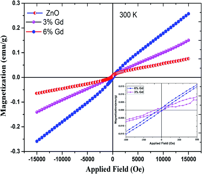 |
| | Fig. 8 Magnetic hysteresis (M–H) curves for pure, 3% and 6% Gd-doped ZnO. The inset figure shows their magnified loop. | |
RTFM with high magnetization was expected in Gd-doped ZnO system. The idea behind this anticipation is the ferromagnetic nature of Gd up to ∼289 K.60 However, the mechanism responsible for the detected ferromagnetism at room temperature in DMSs is still controversial. The presence of Gd-clusters or secondary phase of Gd2O3, which is quite often found in DMSs and not being detectable by XRD measurement, should yield either a large paramagnetic or very soft-FM hysteresis loop. It has also been reported that the presence of point defects may be responsible for the weak ferromagnetic ordering in the Zn1−xGdxO.77 Bantounas et al.41 utilized density functional theory within the GGA+U formalism to investigate the magnetic ordering and spatial arrangement of Gd impurities in ZnO host lattice. The authors showed that the results were predominantly paramagnetic for Gd-doped ZnO. In a few cases, e.g. magnetic impurities occupying in-plane nearest-neighbor zinc sites with n-type carrier doping, weak ferromagnetic coupling was perceived and can be diminished by thermal fluctuations. On the other hand, Aravindh et al.,40 suggested that the RTFM and high TC in ZnGdO nanowires can be achieved with the presence of O vacancy that leads to stronger s–f coupling. A key characteristic of Gd differentiating it from other rare earth atoms is the partially filled 4f and 5d orbitals, which could activate inter- and intra-ion exchange interactions.99 Thus, there are several magnetic coupling mechanisms responsible for the RTFM in Gd-doped ZnO.100 In addition to the s–f exchange, as the Gd 5d electrons contribute to the conduction band minima (CB), s–d exchange between Gd ions can be mediated by defect band positioned near to the CB edge.101 This defect band has been stated to have spin-split caused by the s–d coupling.102 Therefore, in our case, the s–d coupling between the Gd ions and the ZnO host lattice in the presence of anion or cation vacancies may attribute to the observed weak RTFM. This observation has been confirmed by our DFT+U calculations below.
4.6. Theoretical results
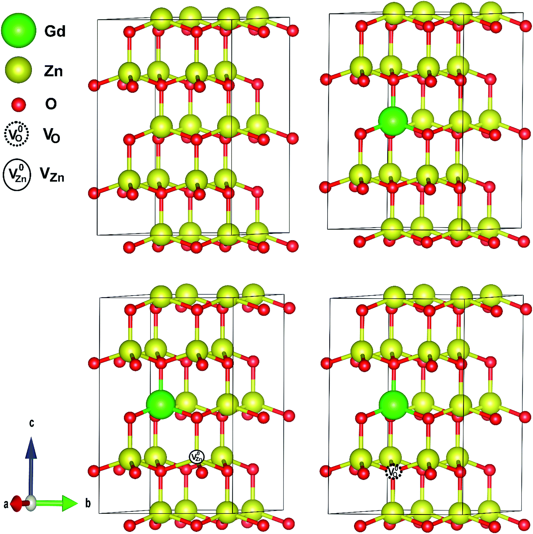
Fig. 9 represents the most stable structure of Gd and complex defects doped ZnO crystal structure. We have conducted spin and non-spin polarization GGA to find the most suitable geometrical optimization technique. According to the total energy optimizations, we found that the systems with Gd and complex defects doped ZnO prefer the spin-polarized state, which is in good agreement with earlier calculations.41 The observed decrease of the c lattice constant value with Gd content measured by XRD, even with the replacement of Gd on Zn sites, can only be described by the development of Gd-defect complexes. The simulations demonstrate that a- and c-lattice constants expand in Gd-doped ZnO (a = 3.295 Å and c = 5.274 Å) with respect to those of pristine ZnO. For GdZn–VO complex, lattice parameters shrink (a = 3.284 Å and c = 5.261 Å) while the expansion induced by the development of GdZn–VZn complex.
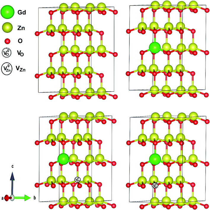 |
| | Fig. 9 Crystal structures of pristine, Gd-doped ZnO and Gd-complex defects ZnO. | |
To validate the thermodynamic stability of the examined defect complexes, we have assessed the formation energy of the crystal system under the coexistence of Gd doping and O vacancy or Zn vacancy using the following expressions.35,103
| | |
ΔEGd = EZnO:Gd − EZnO − μGd + μZn + q(EF)
| (7) |
| | |
ΔEGd+VO = EZnO:Gd+VO − EZnO − μGd + μO + μZn + q(EF)
| (8) |
| | |
ΔEGd+VZn = EZnO:Gd+VZn − EZnO − μGd + 2μZn + q(EF)
| (9) |
where the first and second terms represent the total energy of defect-bearing supercell and pristine structure respectively, whereas
μ signifies the chemical potential of Zn, Gd and O atoms. The chemical potential relies on experimental growth conditions and can be estimated from the total energies of hexagonal bulks Gd
E (Gd
metal), Zn
E (Zn
metal) and gas O
2 E (O
2). Here
q denotes the electron charge, while
EF represents the Fermi energy. Since we are only considering the neutral state in these calculations (
q = 0), the last term is excluded from these equations. Recently, Rosa and Frauenheim
104 have considered the complexes in various charge states, namely −1 and +1 and +2, and they found that these defects are not energetically favorable under O-rich or Zn-rich environments. The formation energies of the neutral Gd and complex defects doped ZnO were calculated under O-rich and Zn-rich conditions. Under O-rich limit,

and
μZn =
EZnO −
EO. Under the Zn-rich limit,
μZn =
E(Zn
metal), and
μO =
EZnO −
EZn. The calculated values of the formation energy of the doped systems under both conditions are tabulated in Table S3.
† The latter shows that all doped systems have negative formation energy, that is, it is experimentally achievable to synthesize the defect-bearing crystal structures.
31 It can be perceived that the formation energy (Δ
EO) is −3.17 eV for Gd incorporation in wurtzite ZnO under O-rich limit which is lower than the value under the Zn-rich environment (Δ
EZn). Therefore, it is easier for Gd replacing Zn atoms under O-rich condition. The estimated values are in line with the previous theoretical reports.
40,103 Under the Zn-rich limit, the Δ
EZn increases either by introducing Zn vacancy or O vacancy. Moreover, the complex system with Zn vacancy has the lowest formation energy under Zn-poor limit. This may suggest that the occurrence of vacancy-dopant complexes is preferred energetically.
95 Thus, Gd doping easily induced V
Zn on the ZnO host lattice. This behavior is consistent with previous theoretical investigation.
105
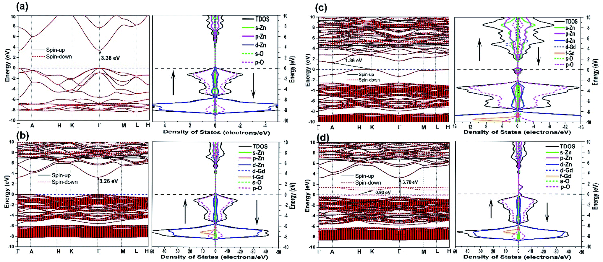
Finally, we discuss the electronic structure of the above mentioned neutral defect-bearing structures. Fig. 10 exhibits the electronic band structures, the total density of states (TDOS), and the partial density of states (PDOS) of pristine and doped ZnO using GGA+U formalism. As presented in Fig. 10(a), the defect-free ZnO structure is a nonmagnetic semiconductor with a direct band gap of 3.38 eV positioned at Γ–Γ′ points, which agrees well with the previous experimental and theoretical values.8,106 The calculated value confirms the presence of point defects as compared to our observed band gap (2.66 eV) using UV-vis spectrometer. One may also observe that the spin-up and spin-down channels are well overlapped, indicating the nonmagnetic behavior of the pristine structure. The PDOS reveals that the conduction band minima (CB) of ZnO is composed essentially of Zn-4s states and some overlapping between Zn-3d and O-2p, and the valence band maxima (VB) is dominated by the O-2p states with a minor contribution of Zn-3d states. However, the contribution of Zn-d states becomes prominent in the −6 to −8 eV range. The band gap of doped ZnO becomes slightly narrower (3.26 eV) due to the incorporation of Gd ions into the host last, see Fig. 10(b). This confirms that the experimental increasing of the band gap is due to the Burstein–Moss shift. One may observe a trivial spin split of the conduction band edge which indicates the magnetic behavior of the doped host lattice. As demonstrated in Fig. 10(b), the TDOS and PDOS of the doped ZnO show that the spin-up and spin-down channels are asymmetric, reveal the Zn15GdO16 is a magnetic semiconductor with a total magnetic moment of ∼7 μB. The PDOS demonstrates that bottom of conduction band mainly composed of 5d and 4s states, while the 4f states are about 15 eV above the Fermi level (not shown here). On the other hand, the top of the VB is similar to that of the pristine structure except for the presence of 4f states at −7 eV. This observation is in good agreement with the previous theoretical report.101 Ferromagnetic ordering takes place when the Fermi level is positioned close to the band edge and overlaps with the impurity level. Consequently, it can be partially occupied by the donor/acceptor electrons and magnetic exchange coupling be able to occur.107 For GdZn–VO complex, the band gap value was significantly decreased compared to that of pristine and Gd-doped ZnO, see Fig. 10(c). The presence of O-vacancy (donors), which induces two electrons to the system, has an effect on the location of valance band maxima and the bottom of the conduction band to give an indirect band gap of 1.36 eV located at K–A′ points. This type of complex defect induced a new defect band levels (Zn-3p and 4s states) in the vicinity of the Fermi level. The strong hybridization between the Gd-5d and Zn-4s can shift some of the energy bands downward into the state of low energy. For the GdZn–VZn (Fig. 10(d)), band structures display robust spin splitting between the majority- and minority-spin states close the Fermi level, which suggests that this type of complex defect can induce ferromagnetism in the ZnO hosts. Two impurity levels, one at the top of the valence band and the other one equals to 1.4 eV above Fermi level, are formed in the band gap. The introduction of Zn vacancy (acceptors), which induces two holes to the system, causes the energy band gap to decrease down to 0.93 eV in the spin-down state whereas it displays wide gap semiconductor character (3.70 eV) in the spin-up direction. The difference in the energy gaps between the spin-up and spin-down states indicates that GdZn–VZn complex doped ZnO is spin-filter semiconductors. Furthermore, TDOS and PDOS of the doped ZnO reveal robust asymmetric between the spin-up and spin-down channels, resulting in magnetism in the Zn14GdO16 structure. The magnetic moment of the doped crystal structure has been increased. This indicates that the GdZn–VZn complex can effectively mediate the ferromagnetic ordering of the doped system. This observation is in good agreement with the conclusion suggested by Bantounas et al.108 The increase of acceptor level (VZn) upon Gd3+ doping has been experimentally reported by Reddy et al.109 and Vijayaprasath et al.60 As a result, the prospect of having Gd-p-type as well as Gd-n-type ferromagnetic semiconductors could uncover a wide range of new potential materials and new possible applications of DMSs.
 |
| | Fig. 10 The electronic band structures, TDOS and PDOS of (a) pristine ZnO, (b) Gd-doped ZnO, (c) GdZn–VO complex and (d) GdZn–VZn complex. | |
5. Conclusions
In summary, pristine and Gd-doped ZnO-NRs have been successfully prepared via thermal decomposition method. The incorporation of the gadolinium in the ZnO nanostructure was verified by X-ray diffraction. The morphologies and the elemental composition of the synthesized products were revealed by TEM and FSEM plus EDX techniques. The optical absorption spectrum of pure ZnO was enhanced at 6% Gd amount. The magnetic features were found to change with varying dopant concentration. The photoluminescence at room temperature demonstrates the existence of defects which further increases with increase in Gd doping. To perform an in-depth analysis of the electronic structures and the physical mechanism of these materials at the atomic scale, DFT+U calculations have been employed. Hole carries significantly affect the magnetic behavior of the doped system. This diluted magnetic semiconducting nanoparticles can be suitable for magneto-optoelectronic applications.
Conflicts of interest
There are no conflicts to declare.
References
- S. Kumar and P. Sahare, Gd3+ incorporated ZnO nanoparticles: a versatile material, Mater. Res. Bull., 2014, 51, 217–223 CrossRef CAS.
- M. Isik and N. Gasanly, Gd-doped ZnO nanoparticles: synthesis, structural and thermoluminescence properties, J. Lumin., 2019, 207, 220–225 CrossRef CAS.
- Z. Liu, et al, Ferromagnetism and its stability in n-type Gd-doped GaN: first-principles calculation, Appl. Phys. Lett., 2012, 100, 232408 CrossRef.
- Y. Zhang, H.-L. Shi, S. Wang, P. Zhang and R. Li, Electronic structure and magnetic coupling properties of Gd-doped AlN: first-principles calculations, Eur. Phys. J. B, 2010, 77, 345–349 CrossRef CAS.
- M. Zeghouane, et al, Selective Growth of Ordered Hexagonal InN Nanorods, CrystEngComm, 2019, 21, 2702–2708 RSC.
- K. Wu, H. He, Y. Lu, J. Huang and Z. Ye, Dominant free exciton emission in ZnO nanorods, Nanoscale, 2012, 4, 1701–1706 RSC.
- S. Sönmezoğlu and E. Akman, Improvement of physical properties of ZnO thin films by tellurium doping, Appl. Surf. Sci., 2014, 318, 319–323 CrossRef.
- C.-T. Lee, Fabrication Methods and Luminescent Properties of ZnO Materials for Light-Emitting Diodes, Materials, 2010, 3, 2218–2259 CrossRef CAS.
- M. Law, L. E. Greene, J. C. Johnson, R. Saykally and P. Yang, Nanowire dye-sensitized solar cells, Nat. Mater., 2005, 4, 455 CrossRef CAS.
- M. H. Huang, et al, Room-temperature ultraviolet nanowire nanolasers, Science, 2001, 292, 1897–1899 CrossRef CAS.
- Z. W. Pan, Z. R. Dai and Z. L. Wang, Nanobelts of semiconducting oxides, Science, 2001, 291, 1947–1949 CrossRef CAS.
- C. J. Lee, et al, Field emission from well-aligned zinc oxide nanowires grown at low temperature, Appl. Phys. Lett., 2002, 81, 3648–3650 CrossRef CAS.
- X. Sun, L. Wang and H. Kwok, Improved ITO thin films with a thin ZnO buffer layer by sputtering, Thin Solid Films, 2000, 360, 75–81 CrossRef CAS.
- X. Ma, The magnetic properties of Gd doped ZnO nanowires, Thin Solid Films, 2012, 520, 5752–5755 CrossRef CAS.
- X. Li, et al, Point defects in lines in single crystalline phosphorene: directional migration and tunable band gaps, Nanoscale, 2016, 8, 17801–17808 RSC.
- M. M. Obeid, et al, Analysis of the structural, electronic, elastic and thermodynamic properties of CuAl2X4 (X = O, S) spinel structure, Mater. Res. Bull., 2018, 108, 255–265 CrossRef CAS.
- J. Coey, M. Venkatesan and C. Fitzgerald, Donor impurity band exchange in dilute ferromagnetic oxides, Nat. Mater., 2005, 4, 173 CrossRef CAS.
- X. Wang, et al, Low-temperature growth and properties of ZnO nanowires, Appl. Phys. Lett., 2004, 84, 4941–4943 CrossRef CAS.
- J. Q. Hu, Q. Li, X. Meng, C. Lee and S. Lee, Thermal reduction route to the fabrication of coaxial Zn/ZnO nanocables and ZnO nanotubes, Chem. Mater., 2003, 15, 305–308 CrossRef CAS.
- J.-J. Wu and S.-C. Liu, Catalyst-free growth and characterization of ZnO nanorods, J. Phys. Chem. B, 2002, 106, 9546–9551 CrossRef CAS.
- X. Wang, Y. Ding, C. J. Summers and Z. L. Wang, Large-scale synthesis of six-nanometer-wide ZnO nanobelts, J. Phys. Chem. B, 2004, 108, 8773–8777 CrossRef CAS.
- M. Zheng, L. Zhang, G. Li and W. Shen, Fabrication and optical properties of large-scale uniform zinc oxide nanowire arrays by one-step electrochemical deposition technique, Chem. Phys. Lett., 2002, 363, 123–128 CrossRef CAS.
- Y. Zhang, et al, Synthesis of nano/micro zinc oxide rods and arrays by thermal evaporation approach on cylindrical shape substrate, J. Phys. Chem. B, 2005, 109, 13091–13093 CrossRef CAS.
- J. Jie, et al, Synthesis and characterization of aligned ZnO nanorods on porous aluminum oxide template, J. Phys. Chem. B, 2004, 108, 11976–11980 CrossRef CAS.
- H. Le, S. Chua, K. Loh, E. Fitzgerald and Y. Koh, Synthesis and optical properties of well aligned ZnO nanorods on GaN by hydrothermal synthesis, Nanotechnology, 2005, 17, 483 CrossRef.
- H. Zhang, J. Feng, J. Wang and M. Zhang, Preparation of ZnO nanorods through wet chemical method, Mater. Lett., 2007, 61, 5202–5205 CrossRef CAS.
- A. Kiani, K. Dastafkan, A. Obeydavi and M. Rahimi, Solid solutions of gadolinium doped zinc oxide nanorods by combined microwave-ultrasonic irradiation assisted crystallization, Solid State Sci., 2017, 74, 152–167 CrossRef CAS.
- Y. Luo, et al, Fabrication and photocatalytic properties of Gd-doped ZnO nanoparticle-assembled nanorods, Mater. Lett., 2015, 149, 70–73 CrossRef CAS.
- N. Sarip et al, in Applied Mechanics and Materials, Trans Tech Publ, 2015, pp. 734–738 Search PubMed.
- M. M. Obeid, et al, The electronic, half-metallic, and magnetic properties of Ca1−xCrxS ternary alloys: insights from the first-principle calculations, J. Mol. Graphics Modell., 2019, 89, 22–32 CrossRef CAS.
- M. M. Obeid, S. J. Edrees and M. M. Shukur, Synthesis and characterization of pure and cobalt doped magnesium oxide nanoparticles: insight from experimental and theoretical investigation, Superlattices Microstruct., 2018, 122, 124–139 CrossRef CAS.
- R. Saravanan, K. Santhi, N. Sivakumar, V. Narayanan and A. Stephen, Synthesis and characterization of ZnO and Ni doped ZnO nanorods by thermal decomposition method for spintronics application, Mater. Charact., 2012, 67, 10–16 CrossRef CAS.
- K. R. Kittilstved, et al, Direct kinetic correlation of carriers and ferromagnetism in Co2+: ZnO, Phys. Rev. Lett., 2006, 97, 037203 CrossRef.
- S. Kumar, et al, Insight into the origin of ferromagnetism in Fe-doped ZnO diluted magnetic semiconductor nanocrystals: an EXFAS study of local structure, RSC Adv., 2015, 5, 94658–94669 RSC.
- Q. Hou, Z. Xu, X. Jia and C. Zhao, Effects of Ni doping and native point defects on magnetism of ZnO first-principles study, J. Appl. Phys., 2018, 123, 055106 CrossRef.
- H. Cao, et al, First-principles study on electronic and magnetic properties of (Mn, Fe)-codoped ZnO, J. Magn. Magn. Mater., 2014, 352, 66–71 CrossRef CAS.
- Q. Chen and J. Wang, Ferromagnetism in Nd-doped ZnO nanowires and the influence of oxygen vacancies: ab initio calculations, Phys. Chem. Chem. Phys., 2013, 15, 17793–17797 RSC.
- K. Potzger, et al, Ferromagnetic Gd-implanted ZnO single crystals, J. Appl. Phys., 2006, 99, 063906 CrossRef.
- M. Ungureanu, et al, A comparison between ZnO films doped with 3d and 4f magnetic ions, Thin Solid Films, 2007, 515, 8761–8763 CrossRef CAS.
- S. A. Aravindh, U. Schwingenschloegl and I. S. Roqan, Ferromagnetism in Gd doped ZnO nanowires: a first principles study, J. Appl. Phys., 2014, 116, 233906 CrossRef.
- I. Bantounas, V. Singaravelu, I. S. Roqan and U. Schwingenschlögl, Structural and magnetic properties of Gd-doped ZnO, J. Mater. Chem. C, 2014, 2, 10331–10336 RSC.
- S. Sambasivam, et al, Intense violet–blue emission and paramagnetism of nanocrystalline Gd3+ doped ZnO ceramics, J. Adv. Ceram., 2015, 4, 300–306 CrossRef CAS.
- A. Manikandan, et al, Rare earth element (REE) lanthanum doped zinc oxide (La: ZnO) nanomaterials: synthesis structural optical and antibacterial studies, J. Alloys Compd., 2017, 723, 1155–1161 CrossRef CAS.
- Y. Zhang, G. Zhang and Y. Wang, First-principles study of the electronic structure and optical properties of Ce-doped ZnO, J. Appl. Phys., 2011, 109, 063510 CrossRef.
- A. Chakraborty, C. S. Jong, N. Ganguli and I. Dasgupta, A comparative study of magnetic and optical properties of Mn-, Gd-, and Nd-doped ZnO nanowires, Int. J. Mod. Phys. B, 2017, 31, 1650241 CrossRef CAS.
- M. M. Obeid, et al, Electronic Band Structure, Thermodynamics and Optical Characteristics of BeO1−xAx (A = S, Se, Te) Alloys: Insights from Ab Initio Study, Chem. Phys., 2019, 526, 110414 CrossRef CAS.
- H. R. Jappor, et al, Engineering the optical and electronic properties of Janus monolayer Ga2SSe by biaxial strain, Superlattices Microstruct., 2019, 130, 545–553 CrossRef CAS.
- D. Hoat, T. V. Vu, M. M. Obeid and H. R. Jappor, Assessing optoelectronic properties of PbI2 monolayer under uniaxial strain from first principles calculations, Superlattices Microstruct., 2019, 130, 354–360 CrossRef CAS.
- S. J. Edrees, M. M. Shukur and M. M. Obeid, First-principle analysis of the structural, mechanical, optical and electronic properties of wollastonite monoclinic polymorph, Computational Condensed Matter, 2018, 14, 20–26 CrossRef.
- M. M. Obeid, et al, Electronic and magnetic properties of single-layer boron phosphide associated with materials processing defects, Comput. Mater. Sci., 2019, 170, 109201 CrossRef CAS.
- D. Hoat, T. V. Vu, M. M. Obeid and H. R. Jappor, Tuning the Electronic Structure of 2D Materials by Strain and External Electric Field: Case of GeI2 Monolayer, Chem. Phys., 2019, 527, 110499 CrossRef CAS.
- H. T. Nguyen, et al, Strain-tunable electronic and optical properties of monolayer GeSe: promising for photocatalytic water splitting applications, Chem. Phys., 2019, 529, 110543 CrossRef.
- S. J. Clark, et al, First principles methods using CASTEP, Z. Kristallogr. - Cryst. Mater., 2005, 220, 567–570, DOI:10.1524/zkri.220.5.567.65075.
- G. Kresse and D. Joubert, From ultrasoft pseudopotentials to the projector augmented-wave method, Phys. Rev. B: Condens. Matter Mater. Phys., 1999, 59, 1758, DOI:10.1103/physrevB.59.1758.
- A. Stashans and K. Rivera, Electronic and Magnetic Properties of Co-and Mn-codoped ZnO by Density Functional Theory, Chin. Phys. Lett., 2016, 33, 097102 CrossRef.
- T. H. Flemban, et al, Identifying the influence of the intrinsic defects in Gd-doped ZnO thin-films, J. Appl. Phys., 2016, 119, 065301 CrossRef.
- E. Goh, J. Mah and T. Yoon, Effects of Hubbard term correction on the structural parameters and electronic properties of wurtzite ZnO, Comput. Mater. Sci., 2017, 138, 111–116 CrossRef CAS.
- A. Dakhel and M. El-Hilo, Ferromagnetic nanocrystalline Gd-doped ZnO powder synthesized by coprecipitation, J. Appl. Phys., 2010, 107, 123905 CrossRef.
- A. Khataee, R. D. C. Soltani, A. Karimi and S. W. Joo, Sonocatalytic degradation of a textile dye over Gd-doped ZnO nanoparticles synthesized through sonochemical process, Ultrason. Sonochem., 2015, 23, 219–230 CrossRef CAS.
- G. Vijayaprasath, R. Murugan, Y. Hayakawa and G. Ravi, Optical and magnetic studies on Gd doped ZnO nanoparticles synthesized by co-precipitation method, J. Lumin., 2016, 178, 375–383 CrossRef CAS.
- S. Kumar, et al, Investigations on structural and optical properties of ZnO and ZnO: Co nanoparticles under dense electronic excitations, RSC Adv., 2014, 4, 62123–62131 RSC.
- S. Goel, et al, Ferroelectric Gd-doped ZnO nanostructures: enhanced dielectric, ferroelectric and piezoelectric properties, Mater. Chem. Phys., 2017, 202, 56–64 CrossRef CAS.
- S. Goel, N. Sinha, H. Yadav, A. J. Joseph and B. Kumar, Experimental investigation on the structural, dielectric, ferroelectric and piezoelectric properties of La doped ZnO nanoparticles and their application in dye-sensitized solar cells, Phys. E, 2017, 91, 72–81 CrossRef CAS.
- A. S. H. Hameed, et al, Impact of alkaline metal ions Mg2+, Ca2+, Sr2+ and Ba2+ on the structural, optical, thermal and antibacterial properties of ZnO nanoparticles prepared by the co-precipitation method, J. Mater. Chem. B, 2013, 1, 5950–5962 RSC.
- D. Arora, K. Asokan, A. Mahajan, H. Kaur and D. Singh, Structural, optical and magnetic properties of Sm doped ZnO at dilute concentrations, RSC Adv., 2016, 6, 78122–78131 RSC.
- S. Kumar and R. Thangavel, Gd doping effect on structural, electrical and magnetic properties of ZnO thin films synthesized by sol-gel spin coating technique, Electron. Mater. Lett., 2017, 13, 129–135 CrossRef CAS.
- D. Mithal and T. Kundu, Effect of Gd3+ doping on structural and optical properties of ZnO nanocrystals, Solid State Sci., 2017, 68, 47–54 CrossRef CAS.
- M. Faraz, F. K. Naqvi, M. Shakir and N. Khare, Synthesis of samarium-doped zinc oxide nanoparticles with improved photocatalytic performance and recyclability under visible light irradiation, New J. Chem., 2018, 42, 2295–2305 RSC.
- R. L. d. S. e Silva, P. Banerjee and A. F. Júnior, Functional properties of donor-and acceptor-co-doped high dielectric constant zinc oxide ceramics, Phys. Chem. Chem. Phys., 2019, 21, 9456–9464 RSC.
- D. K. Dubey, et al, Local structure and photocatalytic properties of sol–gel derived Mn–Li co-doped ZnO diluted magnetic semiconductor nanocrystals, RSC Adv., 2016, 6, 22852–22867 RSC.
- M. Gaudon, O. Toulemonde and A. Demourgues, Green coloration of Co-doped ZnO explained from structural refinement and bond considerations, Inorg. Chem., 2007, 46, 10996–11002 CrossRef CAS.
- J. Beltrán, C. Barrero and A. Punnoose, Understanding the role of iron in the magnetism of Fe doped ZnO nanoparticles, Phys. Chem. Chem. Phys., 2015, 17, 15284–15296 RSC.
- G. Dillip, A. Banerjee and S. Joo, Conductivity inversion of ZnO nanoparticles in ZnO-carbon nanofiber hybrid thin film devices by surfactant-assisted C-doping and non-rectifying, non-linear electrical properties via interfacial trap-induced tunneling for stress-grading applications, J. Appl. Phys., 2019, 125, 175106 CrossRef.
- Y. Chen, et al, Defects in carbon-rich ferrite of cold-drawn pearlitic steel wires, Metall. Mater. Trans. A, 2013, 44, 3882–3889 CrossRef CAS.
- S. Murugesan, R. Thirumurugesan, E. Mohandas and P. Parameswaran, X-ray diffraction Rietveld analysis and Bond Valence analysis of nano titania containing oxygen vacancies synthesized via sol-gel route, Mater. Chem. Phys., 2019, 225, 320–330 CrossRef CAS.
- S. Khanchandani, S. Kundu, A. Patra and A. K. Ganguli, Shell thickness dependent photocatalytic properties of ZnO/CdS core–shell nanorods, J. Phys. Chem. C, 2012, 116, 23653–23662 CrossRef CAS.
- P. Kaur, et al, Investigations on structural, magnetic and electronic structure of Gd-doped ZnO nanostructures synthesized using sol–gel technique, Appl. Phys. A: Mater. Sci. Process., 2016, 122, 161 CrossRef.
- A. Hassanien, A. A. Akl and A. Sáaedi, Synthesis, crystallography, microstructure, crystal defects, and morphology of BixZn1−xO nanoparticles prepared by sol–gel technique, CrystEngComm, 2018, 20, 1716–1730 RSC.
- P. Bindu and S. Thomas, Estimation of lattice strain in ZnO nanoparticles: X-ray peak profile analysis, Journal of Theoretical and Applied Physics, 2014, 8, 123–134 CrossRef.
- C.-C. Lin and Y.-Y. Li, Synthesis of ZnO nanowires by thermal decomposition of zinc acetate dihydrate, Mater. Chem. Phys., 2009, 113, 334–337 CrossRef CAS.
- A. Sahai and N. Goswamiin AIP Conference Proceedings, AIP Publishing, 2015, p. 050023 Search PubMed.
- A. A. Chaaya, et al, Evolution of microstructure and related optical properties of ZnO grown by atomic layer deposition, Beilstein J. Nanotechnol., 2013, 4, 690–698 CrossRef.
- A. K. Rana, et al, Enhancement of two photon absorption with Ni doping in the dilute magnetic semiconductor ZnO crystalline nanorods, Appl. Phys. Lett., 2015, 107, 231907 CrossRef.
- E. Goh, X. Xu and P. McCormick, Effect of particle size on the UV absorbance of zinc oxide nanoparticles, Scr. Mater., 2014, 78, 49–52 CrossRef.
- S. K. Mishra, R. K. Srivastava and S. Prakash, ZnO nanoparticles: structural, optical and photoconductivity characteristics, J. Alloys Compd., 2012, 539, 1–6 CrossRef CAS.
- E. A. Meulenkamp, Synthesis and growth of ZnO nanoparticles, J. Phys. Chem. B, 1998, 102, 5566–5572 CrossRef CAS.
- M. Mazhdi and M. Tafreshi, The effects of gadolinium doping on the structural, morphological, optical, and photoluminescence properties of zinc oxide nanoparticles prepared by co-precipitation method, Appl. Phys. A: Mater. Sci. Process., 2018, 124, 863 CrossRef.
- D. Sun, H.-J. Sue and N. Miyatake, Optical properties of ZnO quantum dots in epoxy with controlled dispersion, J. Phys. Chem. C, 2008, 112, 16002–16010 CrossRef CAS.
- A. Chanda, et al, Study of structural, optical and magnetic properties of cobalt doped ZnO nanorods, RSC Adv., 2017, 7, 50527–50536 RSC.
- T. Wang, et al, Synthesis of 1D and heavily doped Zn1−xCoxO six-prism nanorods: improvement
of blue–green emission and room temperature ferromagnetism, J. Mater. Chem., 2011, 21, 18810–18816 RSC.
- S. Das, S. Das, A. Roychowdhury, D. Das and S. Sutradhar, Effect of Gd doping concentration and sintering temperature on structural, optical, dielectric and magnetic properties of hydrothermally synthesized ZnO nanostructure, J. Alloys Compd., 2017, 708, 231–246 CrossRef CAS.
- A. Achour, et al, Orange/Red Photoluminescence Enhancement Upon SF6 Plasma Treatment of Vertically Aligned ZnO Nanorods, Nanomaterials, 2019, 9, 794 CrossRef CAS.
- A.-H. Tang, Z.-X. Mei, Y.-N. Hou and X.-L. Du, Photodynamics of GaZn–VZn complex defect in Ga-doped ZnO, Chin. Phys. B, 2018, 27, 117802 CrossRef CAS.
- J. Yi, et al, Ferromagnetism in dilute magnetic semiconductors through defect engineering: Li-doped ZnO, Phys. Rev. Lett., 2010, 104, 137201 CrossRef CAS PubMed.
- J. Qi, et al, Magnetic properties of Er-doped ZnO films prepared by reactive magnetron sputtering, Appl. Phys. A: Mater. Sci. Process., 2010, 100, 79–82 CrossRef CAS.
- B. Poornaprakash, K. Subramanyam, S. P. Vattikuti and M. S. P. Reddy, Achieving enhanced ferromagnetism in ZnTbO nanoparticles through Cu co-doping, Ceram. Int., 2019, 45, 16347–16352 CrossRef CAS.
- B. Poornaprakash, U. Chalapathi, S. Babu and S.-H. Park, Structural, morphological, optical, and magnetic properties of Gd-doped and (Gd, Mn) co-doped ZnO nanoparticles, Phys. E, 2017, 93, 111–115 CrossRef CAS.
- I. S. Roqan, et al, Obtaining strong ferromagnetism in diluted Gd-doped ZnO thin films through controlled Gd-defect complexes, J. Appl. Phys., 2015, 117, 073904 CrossRef.
- H.-S. Li, Y. Li and J. Coey, RT and RR exchange interactions in the rare-earth (R)-transition-metal (T) intermetallics: an evaluation from relativistic atomic calculations, J. Phys.: Condens. Matter, 1991, 3, 7277 CrossRef CAS.
- S. Venkatesh, et al, Defect-band mediated ferromagnetism in Gd-doped ZnO thin films, J. Appl. Phys., 2015, 117, 013913 CrossRef.
- G. Caroena, W. Machado, J. Justo and L. Assali, Lanthanide impurities in wide bandgap semiconductors: a possible roadmap for spintronic devices, Appl. Phys. Lett., 2013, 102, 062101 CrossRef.
- G. M. Dalpian and S.-H. Wei, Electron-mediated ferromagnetism and negative s−d exchange splitting in semiconductors, Phys. Rev. B: Condens. Matter Mater. Phys., 2006, 73, 245204 CrossRef.
- A. A. S. Devi and I. S. Roqan, Analysis on the energetics, magnetism and electronic properties in a 45° ZnO grain boundary doped with Gd, RSC Adv., 2018, 8, 13850–13856 RSC.
- A. Rosa and T. Frauenheim, Electronic structure of gadolinium complexes in ZnO in the GW approximation, J. Magn. Magn. Mater., 2018, 452, 35–39 CrossRef CAS.
- C. Li, Q. Hou, Z. Xu, X. Jia and W. Li, Magnetic Properties of La-Doped ZnO (0001)–Zn Polar Surface with and without Vacancies: a First-Principle Study, J. Supercond. Novel Magn., 2018, 31, 2897–2905 CrossRef CAS.
- X. Ma, Y. Wu, Y. Lv and Y. Zhu, Correlation effects on lattice relaxation and electronic structure of ZnO within the GGA+U formalism, J. Phys. Chem. C, 2013, 117, 26029–26039 CrossRef CAS.
- L. Liu, Y. Y. Peter, Z. Ma and S. S. Mao, Ferromagnetism in GaN:Gd: a density functional theory study, Phys. Rev. Lett., 2008, 100, 127203 CrossRef.
- I. Bantounas, et al, Ab initio investigation on the magnetic ordering in Gd doped ZnO, J. Appl. Phys., 2011, 109, 083929 CrossRef.
- G. Krishna Reddy, A. Jagannatha Reddy, R. Hari Krishna, B. Nagabhushana and G. R. Gopal, Luminescence and spectroscopic investigations on Gd3+ doped ZnO nanophosphor, Journal of Asian Ceramic Societies, 2017, 5, 350–356 CrossRef.
Footnote |
| † Electronic supplementary information (ESI) available. See DOI: 10.1039/c9ra04750f |
|
| This journal is © The Royal Society of Chemistry 2019 |
Click here to see how this site uses Cookies. View our privacy policy here. 
 Open Access Article
 This Open Access Article is licensed under a Creative Commons Attribution-Non Commercial 3.0 Unported Licence
 *a,
Hamad R. Japporb,
Kutaiba Al-Marzokia,
Imad Ali Al-Hydarya,
Shaker J. Edrees
*a,
Hamad R. Japporb,
Kutaiba Al-Marzokia,
Imad Ali Al-Hydarya,
Shaker J. Edrees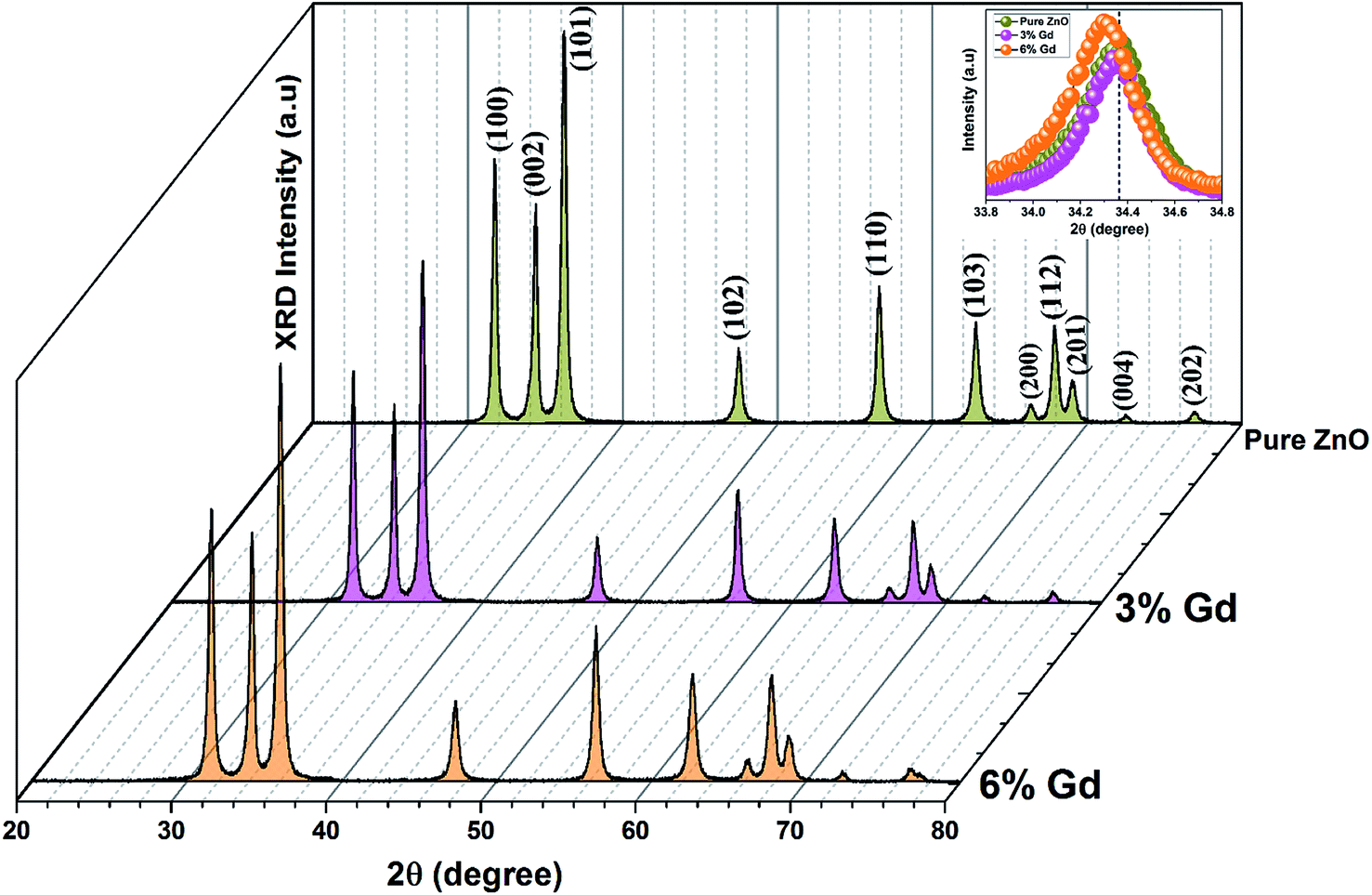
 64 In our refined XRD patterns, the lattice parameters (a, c and V) show a reverse trend where both a and c lattice constants were decreased upon Gd addition (Fig. 3(a) and (b)). This may be attributed to several factors, such as the concentration of dopant, defects (vacancies, interstitial, dislocation), external strains developed due to temperature, and the difference between the ionic radii of Gd and Zn ions.65,66 A similar trend has been found for RE-doped ZnO nanoparticles.64,65,67,68 The a, c lattice parameters and the unit cell volumes (V) progressively decrease as Gd doping concentration increases to 0.03 and, then, a becomes constant while c and V values slightly increase with the increment of the doping concentration. The probable clarification of the perceived trend is that for low concentration of Gd3+, the lattice contraction occurs up to a critical concentration caused by the hydrostatic pressure produced by the rare earth dopants located on the surface of the ZnO-NRs. Upon additional increase in dopant concentration, the crystal lattice expands owing to the substitution of Zn atoms in the core due to relatively large ionic radii of Gd3+ ion. The contraction trends of c parameter upon Gd doping has also been reported by Flemban et al.56 and e Silva et al.69 The substitution of Zn2+ in the tetrahedral site of the ZnO host lattice by Gd3+ ions will cause lattice distortion. The perfect wurtzite structure has a hexagonal unit cell with two lattice constants, a and c, with a ratio of c/a = 1.633.70 Deviation of the crystal from the perfect arrangement can be measured in expressions of the degree of distortion
 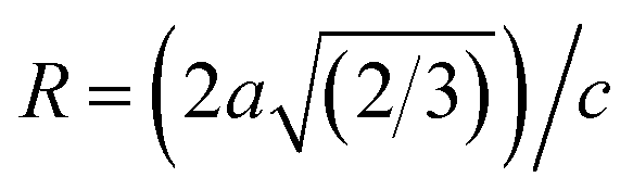 (thus, R = 1 represents no distortion).71 As shown in Fig. 3(c), the c/a ratio and R values were deviated from the ideal value as doping concentration increase, indicating the presence of lattice distortion (anion or cation vacancies).72 Variations of bond lengths with Gd-concentration are illustrated in Fig. 3(d). The variation of bond lengths develops the lattice strain.34 The substitution of Gd atoms in Zn sites attracts oxygen atoms closer, causing elongation of Zn–O bond lengths along c-axis whereas Zn–Zn bond length decreases significantly and then becomes constant at higher doping concentration. Although Zn–O bond length expands along c-axis, it contracts along the a–b axis upon doping (not shown here). We also perceived that the interplanar spacing (d) slightly increased from 2.6028 to 2.6119 Å with an increase of Gd3+ content. This can be attributed to the higher electronegativity of Zn2+ (1.65) compared to that of Gd3+ (1.2), which leads to decrease the attraction force between Gd3+ and O2− than the force between Zn2+ and O2−. Moreover, we have also performed possible non-stoichiometry of anion and cation in the ZnO of both the pristine ZnO-NRs and possible dopant (Gd) concentration at the Zn sites of ZnO host lattice.73 This can be understood from the “Site Occupancy Factor (SOF)” column of Table S1, Fig. S2(a) and (b).† The related discussion of the SOF refinement for prepared products was described in the ESI.†
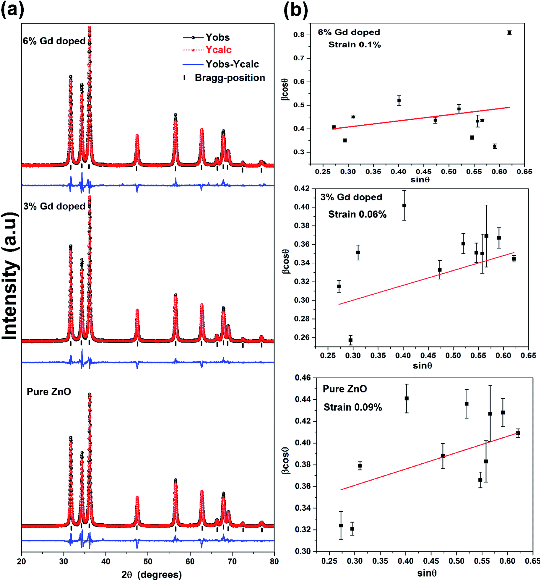


 and μZn = EZnO − EO. Under the Zn-rich limit, μZn = E(Znmetal), and μO = EZnO − EZn. The calculated values of the formation energy of the doped systems under both conditions are tabulated in Table S3.† The latter shows that all doped systems have negative formation energy, that is, it is experimentally achievable to synthesize the defect-bearing crystal structures.31 It can be perceived that the formation energy (ΔEO) is −3.17 eV for Gd incorporation in wurtzite ZnO under O-rich limit which is lower than the value under the Zn-rich environment (ΔEZn). Therefore, it is easier for Gd replacing Zn atoms under O-rich condition. The estimated values are in line with the previous theoretical reports.40,103 Under the Zn-rich limit, the ΔEZn increases either by introducing Zn vacancy or O vacancy. Moreover, the complex system with Zn vacancy has the lowest formation energy under Zn-poor limit. This may suggest that the occurrence of vacancy-dopant complexes is preferred energetically.95 Thus, Gd doping easily induced VZn on the ZnO host lattice. This behavior is consistent with previous theoretical investigation.105