
 Open Access Article
 This Open Access Article is licensed under a Creative Commons Attribution-Non Commercial 3.0 Unported Licence
Electrochemical synthesis of n-type ZnS layers on p-Cu2O/n-ZnO heterojunctions with different deposition temperatures
Rayhena Bengasa,
Halla Lahmarb,
Khelladi Mohamed Redhaa,
Loubna Mentar a,
Amor Azizi*a,
Guy Schmerberc and
Aziz Diniac
a,
Amor Azizi*a,
Guy Schmerberc and
Aziz Diniac
aLaboratoire de Chimie, Ingénierie Moléculaire et Nanostructures, Université Ferhat Abbas-Sétif 1, Algeria. E-mail: amorazizi@univ-setif.dz
bResearch Unit on Nanoscience and Nanotechnology (URNN), Center for the Development of Advanced Technologies (CDTA), Université Ferhat Abbas Sétif 1, 19000 Sétif, Algeria
cInstitut de Physique et Chimie des Matériaux de Strasbourg (IPCMS), UMR 7504 CNRS, Université of Strasbourg, 23 rue du Loess, B.P. 43, 67034 Strasbourg Cedex 2, France
First published on 16th September 2019
Abstract
Metal oxide p–n heterojunctions consisting of p-Cu2O/n-ZnO/n-ZnS nanostructures were deposited on an ITO substrate by three-step electrodeposition. The effect of ZnS layer deposition temperature on the properties of the heterojunction was investigated by different techniques. The Mott–Schottky analysis confirmed the n-type conductivity for ZnO and ZnS and p-type conductivity for the Cu2O layer, respectively. Also, it showed a decrease of ZnS donor concentration with increasing deposition temperature. The X-ray diffraction (XRD) analysis confirms a pure phase of hexagonal ZnO, cubic ZnS and cubic Cu2O structures, respectively. The heterojunction with ZnS deposited at 60 °C shows high crystallinity. The morphological measurements by scanning electron microscopy (SEM) indicate that the deposition temperature has a significant influence on the morphology of ZnO and the atomic force microscopy (AFM) images revealed the improvement of Cu2O morphology by increasing the ZnS deposition temperature. The UV-Vis response shows strong absorption in the visible region and the profile of optical absorption spectra changes with the ZnS deposition temperature. The current–voltage (I–V) characteristics of the Au/p-Cu2O/n-ZnO/n-ZnS/ITO heterojunction display well-defined rectifying behavior for the heterojunction with ZnS deposited at 60 °C.
1. Introduction
In the last 20 years, solar cells based on inorganic materials have been extensively investigated due to their excellent photovoltaic properties.1,2 Cuprous oxide (Cu2O) is a promising candidate material for low-cost solar cell production owing to its low cost, non-toxicity and long-term stability.3,4 Cu2O is a p-type semiconductor with a direct band gap (Eg = 1.9–2.2 eV), and a high absorption coefficient (105 to 106 cm−1) for the photon energies higher than 2.7 eV. In addition, it has a theoretical maximum efficiency of 20% under AMI solar illumination.5 Actually, Cu2O has been employed in many heterojunctions such as CdO/Cu2O, In2O3/Cu2O and ZnO/Cu2O with ZnO as the most successful n-type counterpart.6–8 To date, the highest efficiency of Cu2O based solar cells is 8.1%, obtained for a polycrystalline Cu2O absorber and a Zn1−xGexO buffer layer.9Also, zinc oxide (ZnO) and zinc sulfide (ZnS) are interesting II–IV semiconductors that attract intense attention due to their wide applications in nanodevices and nanosystems, such as solar cells,10 sensors11 and light-emitting diodes.12 The ZnO is n-type semiconductor with wideband gap (3.37 eV), high transparency in the visible range and a large exciton energy (60 meV) at room temperature.13 As well, the ZnS shows a high optical transparency from the ultraviolet (UV) to the infrared (IR) region14 and a large direct band gap of 3.68 eV.15 Compared to the ZnO and ZnS individual layers, ZnO/ZnS heterostructure presents a better electronic, structural and optical properties.16–18 Due to that, the ZnO/ZnS heterostructures have already proved a high potential for application in multi-functional devices such as UV detectors and biological applications.19 Moreover, the theoretical calculation of ZnO/ZnS heterostructures optical properties predicted that such structure could be used as window layer in photovoltaic devices.20 Therefore, such heterostructures are suitable as window layer in Cu2O based solar cells. To our knowledge, the fabrication of Cu2O/ZnO/ZnS by three-step electrochemical deposition has not yet been reported.
Recently, several efforts have been made to provide convenient and efficient approaches for depositing Cu2O based heterojunction. However, these techniques are still too expensive and complicated. As another approach, electrochemical deposition was recognized as competitive method for manufacturing semiconductor thin films due to the following advantages: (i) easy control of the thickness and morphology of the film (ii) simplicity and low equipment cost (iii) the possibility of large area thin films elaboration.
In our group, high quality of ZnO and Cu2O nanostructures were prepared under the optimal condition.21,22 In this study, the Cu2O/ZnO/ZnS heterojunction was prepared by three step electrochemical deposition on indium-doped tin oxide (ITO) substrate. The effect of the deposition temperature of ZnS layer on the structural, morphological, optical and electrical properties of the heterojunction was studied in details.
2. Experimental procedure
The electrochemical deposition of Cu2O/ZnO/ZnS heterojunction was carried out in a typical three-electrode cell using a computer-controlled potentiostat/galvanostat (Voltalab 40) as a potential source. All potentials were reported with reference to the SCE scale. Note that the working electrode was indium tin oxide coated glass (ITO) with sheet resistance of 30 Ω cm−2, a saturated calomel electrode (SCE, +0.241 V vs. SHE) and a platinum electrode were used as reference electrode and counter electrode, respectively. Prior to the electrodeposition the substrates were ultrasonically cleaned with acetone, ethanol and distilled water for 10 min, respectively. The ZnS was directly electrodeposited onto ITO substrate from aqueous electrolyte bath containing 10−4 M ZnSO4 and 10−3 M Na2S2O3, the solution pH was adjusted to 2.4 using sulphuric acid. The deposition temperature of ZnS layers was varied from 40 to 70 °C. Then, the ZnO layer was electrodeposited onto ZnS/ITO substrate by pulse potential deposition with Von of −1.3 V and Voff of −0.1 V were applied during 1 s for 35 cycles.The ZnO deposition bath was containing 0.08 M Zn(NO3)2 and 1 M KNO3 and temperature of 70 °C and pH 6. Then, ZnO/ZnS/ITO was used as substrate for the electrodeposition of Cu2O layer at fixed temperature of 65 °C and applied potential of −0.5 V. The Cu2O deposition bath was containing a 0.05 M of CuSO4 stabilized with 0.05 M citric acid as chelating agent. The pH value was adjusted to 11 using NaOH solution. After the deposition, the samples were washed with distilled water, dried in air and kept for analysis, as show in Fig. 1.
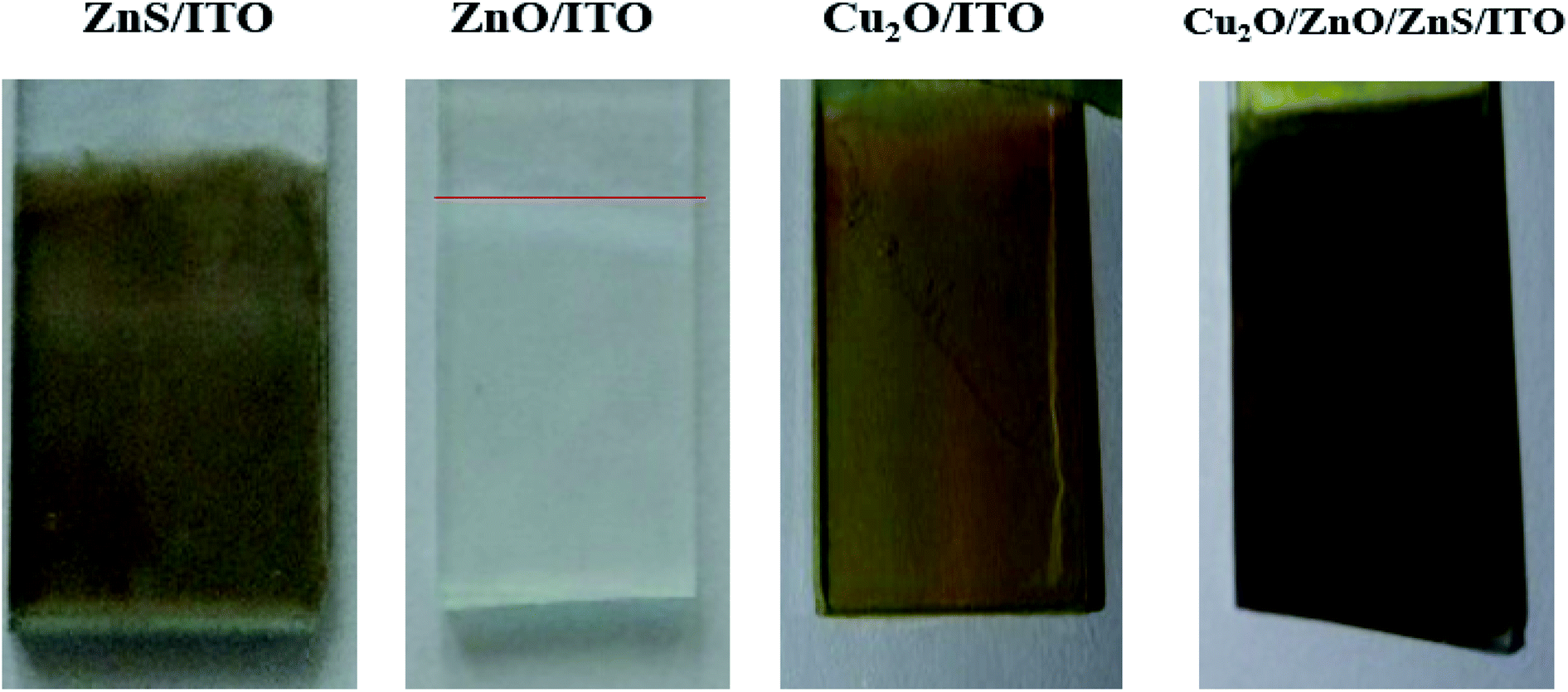 | ||
| Fig. 1 Photographs of ZnS, ZnO, Cu2O individual electrodeposited layers and Cu2O/ZnO/ZnS heterojunction deposited on ITO substrate, respectively. | ||
The thickness (d) of the electrodeposited layers can be estimated from the charge quantity (Q) following Faraday's law:36
 | (1) |
In our study, the thicknesses of ZnO, ZnS and Cu2O layers were fixed at 200, 200 and 300 nm, respectively.
The electrochemical study was carried out using computer-controlled potentiostatic/galvanostatic (Voltalab 40). The Mott–Schottky analysis was realised in 1.0 M KNO3 and employed a frequency of 0.2 kHz for ZnO and ZnS layers and in 0.5 M Na2SO4 solution under applied frequency of 2 kHz for Cu2O layer. Nyquist and Bode electrochemical impedance spectroscopy (EIS) measurements of Cu2O layer and Cu2O/ZnO/ZnS heterojunctions was performed using an alternative current voltage of 10 mV, in a 0.5 M Na2SO4 solution, at frequency range of 105 to 10−2 Hz. The photocurrent response of Cu2O layer and Cu2O/ZnO/ZnS heterojunctions was recorded at −0.5 V vs. SCE in 0.5 M Na2SO4, under chopped irradiation of 500 W xenon (Xe) lamps. The morphological characterization of the films was performed by field emission scanning electron microscopy (FESEM) (JEOL JSM 7000F). The roughness (root-mean-square height deviation) was obtained directly from the software of the AFM (PicoScan 5.3 from molecular imaging) and the crystallographic structure were identified using X-ray diffraction (XRD) Rigaku Smartlab® X-ray diffractometer with a Cu Kα1 radiation (45 kV, 200 mA, λ = 0.154056 nm). The optical properties were investigated using UV-Vis-NIR spectrophotometer (Shimadzu UV-1800) in the UV-visible region. The current–voltage (I–V) measurements were recorded using a picoammeter (Keithley 617) at room temperature in the dark. The ohmic behavior of the electrodes was confirmed by I–V measurement between the gold pads deposited on Cu2O surface and ITO substrate.
3. Results and discussion
3.1 Mott–Schottky analysis
Mott–Schottky analysis (M–S) is well suitable to have information about the semiconductor characteristics, such as the flat band potential and the acceptor/donor concentration without damaging its surface. It is based on examining the semiconductor/solution interface and measuring the capacitance of the semiconductor depletion layer as function of the applied voltage following Mott–Schottky relation.23,24
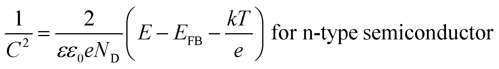 | (2) |
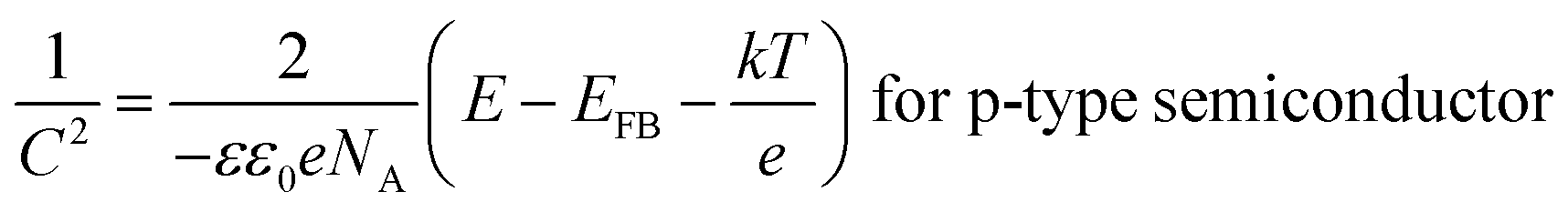 | (3) |
Fig. 2 presents Mott–Schottky plots ZnS layers deposited at different temperatures, ZnO layer and Cu2O layer, respectively. It is clear that the Mott–Schottky equation is valid in a wide range of potential, which indicates well-defined electronic surface states. The M–S plots in Fig. 2a and b reveal straight lines with positive slopes, which confirm the n-type characteristic of ZnS and ZnO layers, respectively. While, the negative slope of M–S plot in Fig. 2c confirms the p-type conductivity of Cu2O layer. In addition, the presence of multiple linear regions in M–S plots of ZnO and ZnS layers indicates the existence of multiple donor levels.27
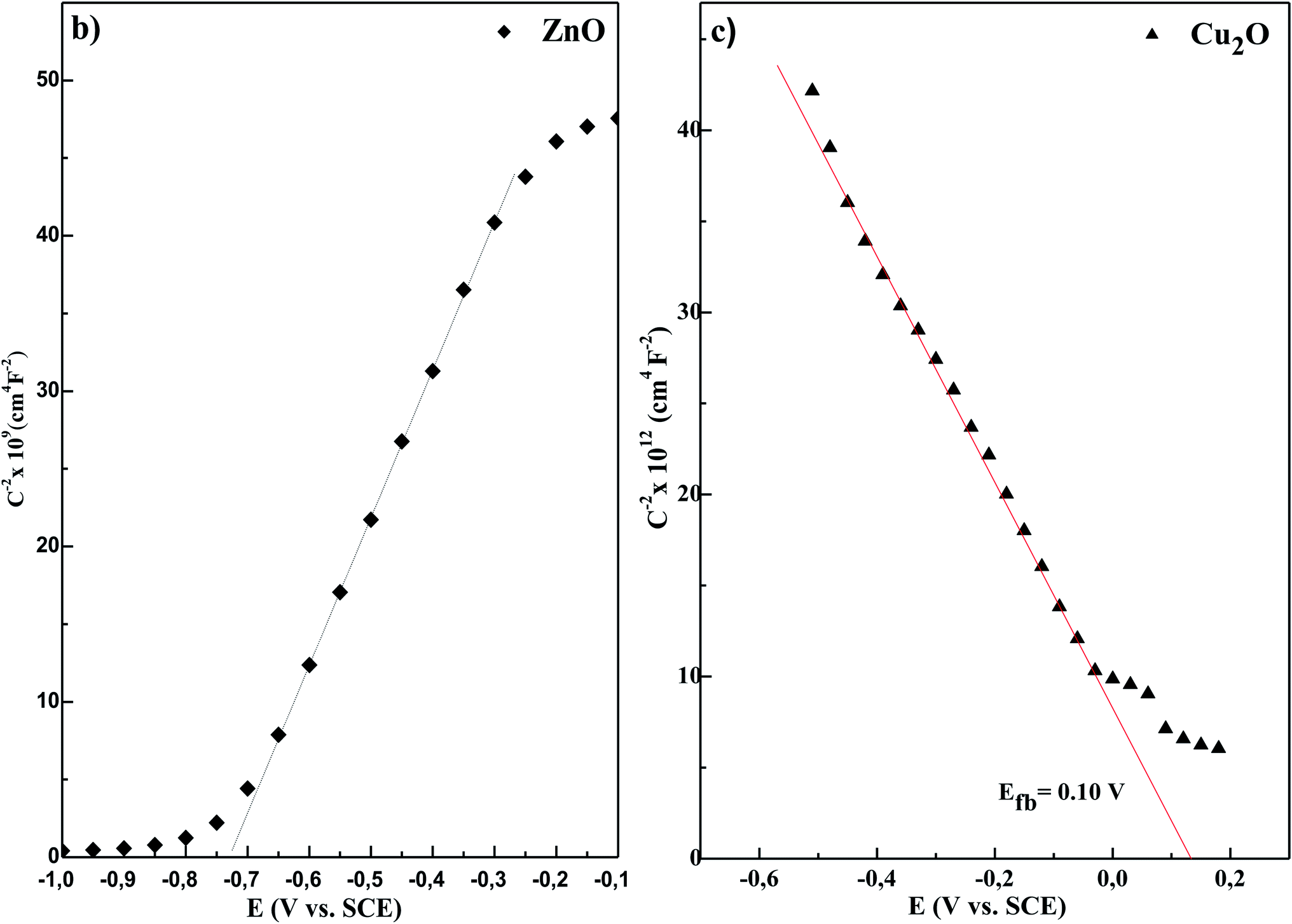 | ||
| Fig. 2 Mott–Schottky plots recorded in 1.0 M KNO3 electrolyte for: (a) ZnS layers deposited at different temperatures, (b) ZnO layer and (c) recorded in 0.5 M Na2SO4 for Cu2O layer. The corresponding flat band potential values are indicated. | ||
The flat band potentials were determined from the extrapolation of the linear portion of M–S plots to  , while the donor and acceptor concentration values were calculated from the slope of M–S plots (
 , the obtained values are set out in Table 1). As can be seen from the data in Table 1, the acceptor concentration was 5.01 × 1017 cm−3 for Cu2O layer, which is within the typical value (1015 to 1018 cm−3) reported in the literature.28 Turning to the ZnO layer, high donor concentration of 1.8 × 1020 cm−3 was obtained, which is in accordance with other studies.29 On the other hand, the ZnS layers show high donor concentration. When the deposition temperature of ZnS increases from 40 to 70 °C, the donor concentration decreases from 2.51 × 10²¹ to 7.28 × 1019 cm−3. Thus, the ZnS layer deposited at higher temperature have the lowest conductivity. This may be due to the higher density of grain boundaries associated with the smaller crystallites size of this sample observed in XRD patterns.30 Accordingly, the flat band potential of ZnS layers increases from −0.94 to −0.51 V vs. SCE with increasing the deposition temperature from 40 to 70 °C, this may be due to the decrease in donor concentration in n-type ZnS layers.31
| Samples | ND,A (cm−3) | Vfb (V per SCE) | Rct (kΩ cm2) |
|---|---|---|---|
| Cu2O/ZnO/ZnS (40 °C) | 2.51 × 10²¹ | −0.94 | 1.088 |
| Cu2O/ZnO/ZnS (50 °C) | 4.94 × 10²⁰ | −0.72 | 0.45 |
| Cu2O/ZnO/ZnS (60 °C) | 5.06 × 10¹⁹ | −0.59 | 0.41 |
| Cu2O/ZnO/ZnS (70 °C) | 7.28 × 10¹⁹ | −0.51 | 0.57 |
| ZnO | 1.80 × 10²⁰ | −0.74 | — |
| Cu2O | 5.01 × 10¹⁷ | +0.10 | — |
3.2 Electrochemical impedance spectroscopy analysis (EIS)
EIS analysis is one of the most common procedures for evaluating the electrical properties of materials due to its extraordinary sensitivity. Fig. 3 presents the Nyquist and Bode diagrams of Cu2O and Cu2O/ZnO/ZnS heterojunctions, with different deposition temperatures of ZnS layer, recorded in 0.5 M Na2SO4 solution and frequency range from 105 to 10−2 Hz. As displayed in Fig. 3a and b, the Nyquist EIS spectra of all samples show semicircle at high frequencies followed by diagonal line at low frequencies (Warburg impedance). It is well known that the semicircle is equal to the charge transfer resistance (Rct), while the diagonal line is related to the diffusion process. In our case, the Warburg line was dominating, in such system, the mass transport is rate limiting due to the high charge-transfer rate and the low rate of charge recombination which will definitely improve the performance of solar cell device.5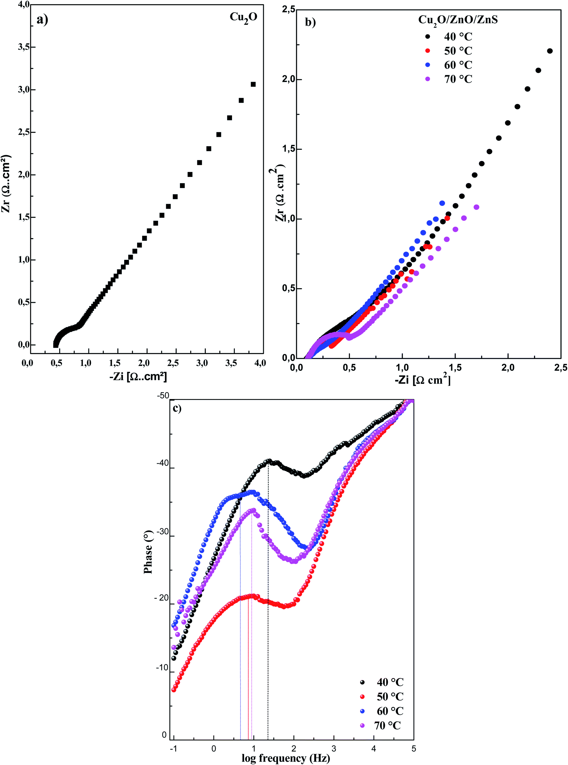 | ||
| Fig. 3 Nyquist EIS diagrams recorded in 0.5 M Na2SO4 solution with a frequency range from 105 Hz to 10−2 Hz for: (a) Cu2O layer and (b) Cu2O/ZnO/ZnS with different deposition temperatures of ZnS layer. (c) Bode EIS plots Cu2O/ZnO/ZnS with different deposition temperatures of ZnS layer. | ||
The reduction in the diameter of semicircle is related to the decrease of the interfacial charge transfer resistance (Rct) across the electrode/electrolyte interface.32 By fitting the Nyquist plots we obtained the charge transfer resistance (Rct) values for Cu2O layer and Cu2O/ZnO/ZnS heterojunctions, with different deposition temperatures of ZnS layer, as summarized in Table 1. It is clear that Rct values of Cu2O/ZnO/ZnS heterojunctions are lower than that of Cu2O layer indicating that the resistance of the charge movement was significantly lower in Cu2O/ZnO/ZnS heterojunction interface. Thus, the Cu2O/ZnO/ZnS heterojunction improves significantly the separation efficiency of photogenerated electron–hole pairs.33 In exception of Cu2O/ZnO/ZnS heterojunctions with ZnS deposited at 40 °C and 70 °C that show Rct higher than Cu2O layer.
Comparing the Rct of Cu2O/ZnO/ZnS heterojunctions, the ZnS deposited at 60 °C reveals the lowest resistance (0.41 × 10³ Ω cm2), which is expected to have a good electrical property compared to others samples.
Fig. 3c presents Bode phase plot of Cu2O/ZnO/ZnS heterojunctions with different deposition temperatures of ZnS layer. In the Bode plot, the peak frequency of the mid-frequency region (1 to 100 Hz) is inversely related to the lifetime of the photogenerated electrons.34,35 Fig. 3c reveals that increasing the deposition temperature of ZnS results in an obvious drop of the peak frequency. The heterojunction with ZnS deposited at 60 °C shows the lowest peak frequency indicating high lifetime of photogenerated electrons. This confirms that the ZnS layer deposited at 60 °C act as an effective surface modification of the window layer to help increase the electron lifetime within the Cu2O/ZnO/ZnS heterojunction.
The separation of photogenerated electron hole pairs in pure Cu2O and Cu2O/ZnO/ZnS heterojunctions will be further investigated in the following section.
3.3 Photoelectrochemical measurements
The photo-activity of pure Cu2O and Cu2O/ZnO/ZnS heterojunction was investigated using photoelectrochemical measurement in order to determine the influence of ZnS deposition temperature on the photo-generation and separation of electron–hole pairs in Cu2O/ZnO/ZnS heterojunction. The transient photocurrent responses performed in 0.5 M Na2SO4 solution and an applied potential of −0.5 V under chopped illumination are shown in Fig. 4.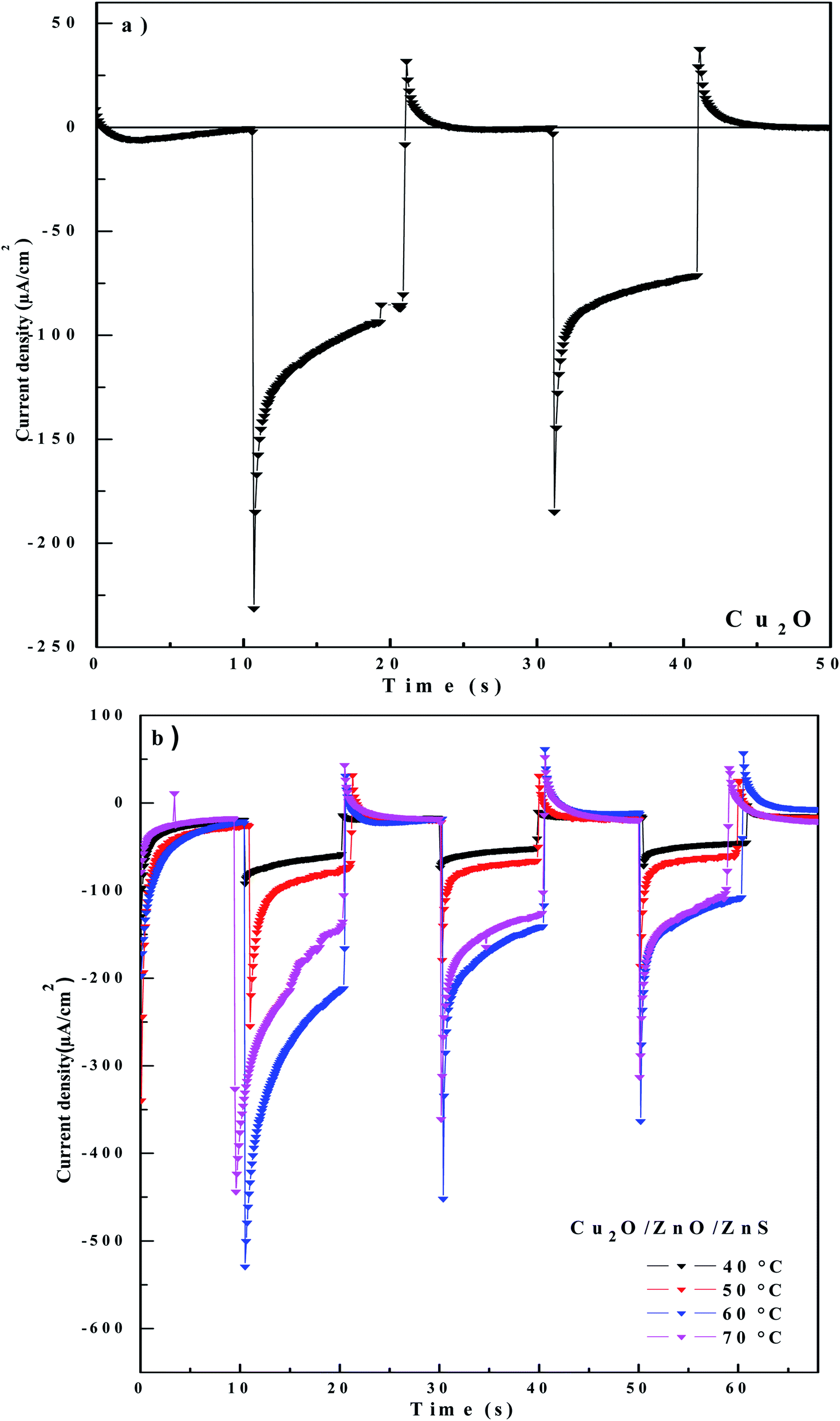 | ||
| Fig. 4 Transient photocurrent response under bias potential of −0.5 V vs. SCE of: (a) Cu2O layer and (b) Cu2O/ZnO/ZnS/ITO heterojunction with different deposition temperatures of ZnS layer. | ||
As can be seen from Fig. 4a, the cathodic photocurrent confirms that Cu2O layer behaves as p-type semiconductor, which is in good agreement with Mott–Schottky plot (Fig. 2c). Under irradiation, the pure Cu2O layer grown on ITO generates photocurrent of 245.6 μA. The deposition of Cu2O on ZnO/ZnS heterostructures at different deposition temperatures caused an increase of photocurrent density. In addition, it can be seen from Fig. 4b that the photocurrent density of the Cu2O deposited onto ZnO/ZnS/ITO layer with different deposited temperatures of ZnS layer high lights a photocurrent value between 78.9 and 480.9 μA. The Cu2O layer deposited on ZnO/ZnS (60 °C)/ITO shows a photocurrent density of 480.9 μA. It is clear that this heterojunction has a better performance compared to pure Cu2O layer and the other samples. Hence, it has a better efficiency of carrier's photo-generation and separation, which is in accord with Nyquist and Bode impedance results reported earlier (Fig. 3b and c).
3.4 Morphological characterization
The surface morphology and topography were examined using scanning electron microscopy (SEM) and atomic force microscopy (AFM) images. Fig. 5a–d present top view SEM images of ZnO layer grown on ZnS/ITO with different deposition temperatures of ZnS layer. It is clear that increasing the deposition temperature of ZnS affects greatly the morphology of ZnO layer. As shown in Fig. 5a, spherical grains of ZnO were spread over the surface of ZnS layer deposited at 40 °C. The higher magnification (insert image) reveals a continuous layer of thin nanosheets of ZnO covering the grains. Increasing the deposition temperature of ZnS to 50 °C (Fig. 5b) increased the size of ZnO grains and we noted the formation of few nanorods of ZnO on ZnS deposited at 60 °C (Fig. 5c). The ZnO forms a dense film of large spherical grain and nanorods covered with thin layer of nanosheets, it is important to note that the size and the number of nanorods increased. Increasing the deposition temperature of ZnS to 70 °C (Fig. 5d) increased the size and amount of ZnO nano-rods and the granular morphology was almost disappeared. It is clear that the amount of ZnO grown on ZnS deposited at 60 °C is higher than other samples and it covered entirely the ZnS surface. This may be due to the high crystallinity of this sample confirmed in XRD measurements. Fig. 6 displays 2D and 3D AFM images of Cu2O/ITO and Cu2O/ZnO/ZnS/ITO with different deposition temperatures of ZnS layer. As shown in Fig. 6a, the Cu2O layer grown on ITO substrate reveals homogenous surface of pyramidal grains with low mean square roughness of 22.5 nm compared to Cu2O layers deposited on ZnO/ZnS/ITO (Fig. 6b–e). On the other hand, the AFM images of Cu2O deposited on ZnO/ZnS/ITO (Fig. 6b–e) show a great effect of ZnS deposition temperature on the morphology of Cu2O. As ZnS deposition temperature increased the surface morphology changed from granular to pyramid shapes. The average surface roughness was 69.2, 65.4, 109.2 and 63.6 nm for of Cu2O layer grown on ZnS deposited at 40, 50, 60 and 70 °C, respectively. The Cu2O grown on ZnS deposited at 60 °C shows the highest roughness (109.2 nm). This value is consistent with the observation. The ZnO deposited on ZnS (60 °C) shows a large grain and good coverage of ZnS surface (insert in Fig. 5c) which facilitates the deposition of Cu2O layer and consequently, the formation of rough surface of Cu2O.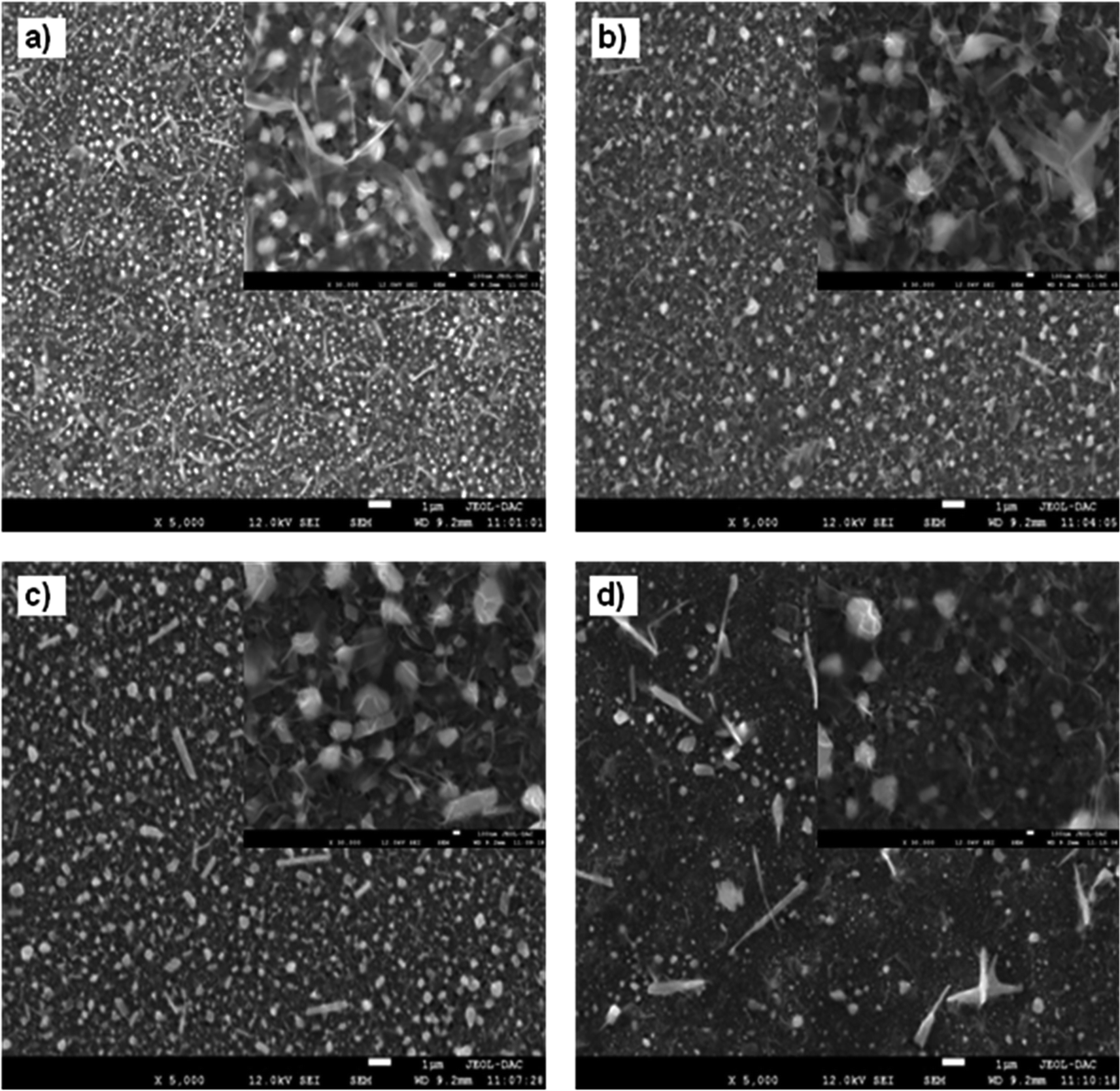 | ||
| Fig. 5 FE-SEM images of ZnO films deposited on ZnS/ITO with different deposition temperatures of ZnS layer: (a) 40 °C, (b) 50 °C, (c) 60 °C and (d) 70 °C. Insert represents the higher magnification of the respective samples. | ||
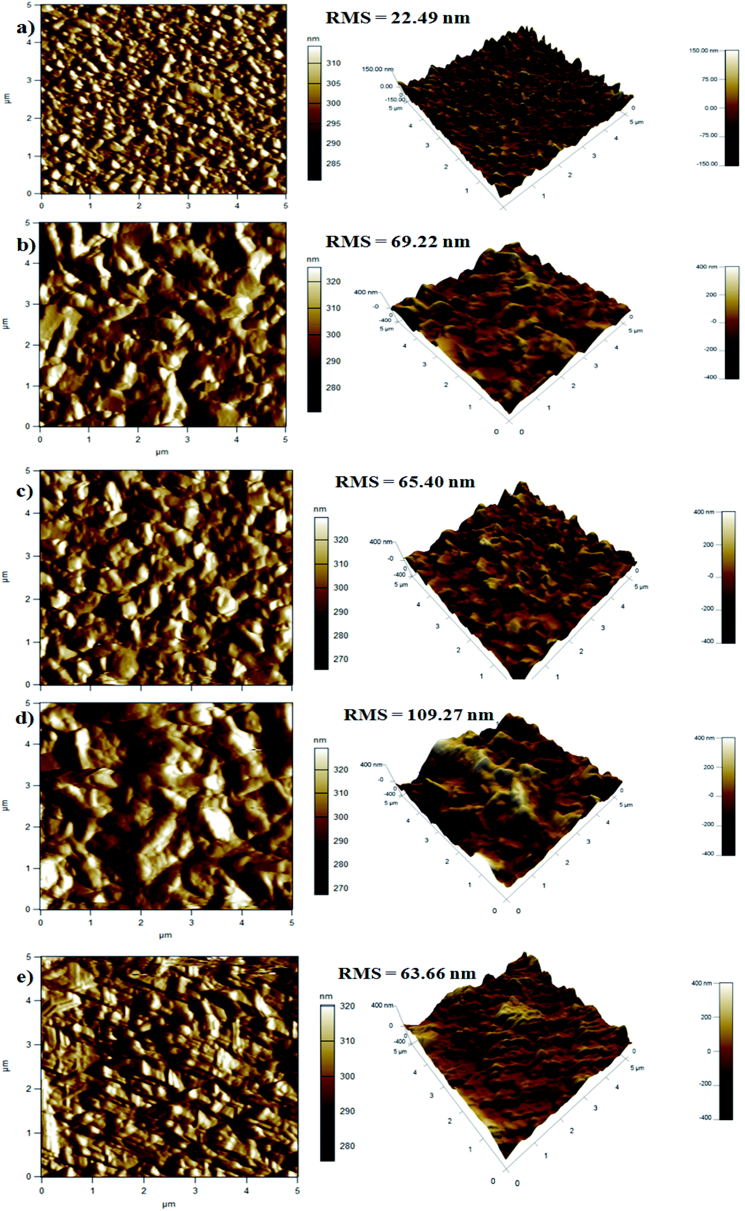 | ||
| Fig. 6 Tapping mode 2D and 3D AFM images (10 × 10 μm2) of: (a) Cu2O/ITO, (b–e) Cu2O/ZnO/ZnS/ITO heterojunctions with different electrodeposition temperatures of ZnS layer: (b) 40 °C, (c) 50 °C, (d) 60 °C and (e) 70 °C. | ||
3.5 Structural characterization
To prove the crystalline structure, X-ray diffraction (XRD) was carried out for Cu2O/ZnO/ZnS/ITO heterojunctions with different deposition temperature of ZnS layer. As shown from XRD pattern in Fig. 7, no impurity peaks were detected besides the diffraction peaks of the indium tin oxide (ITO) substrate (marked by stars in the pattern). The diffraction peaks observed at 2θ ∼ 36.45, 42.22° and 61.35° are indexed respectively to the crystalline orientation (111), (200) and (221) of Cu2O cubic structure (JCPDS card no 00-034-1354). While, the diffraction peak observed at 2θ ∼ 36.45° can be indexed to the crystalline orientation (101) of ZnO hexagonal wurtzite structure according to (JCPDS card no 00-036-1451). Moreover, the supplement diffraction peak at 2θ ∼ 33.01° corresponds to the (200) orientation of cubic ZnS according to the (JCPDS card no 00-005-0566). These results confirm the formation of pure Cu2O/ZnO/ZnS/ITO heterojunctions by three-step electrodeposition process. It is important to note that the preferential orientations are (111), (101) and (200) for Cu2O, ZnO and ZnS, respectively. The presence of different diffraction peaks from basic planes of Cu2O layer indicates that the dense films were composed of Cu2O crystallites with random orientation. The heterojunction with ZnS layer deposited at 60 °C shows the highest of (200) ZnS peak which indicates the high crystallinity of this sample.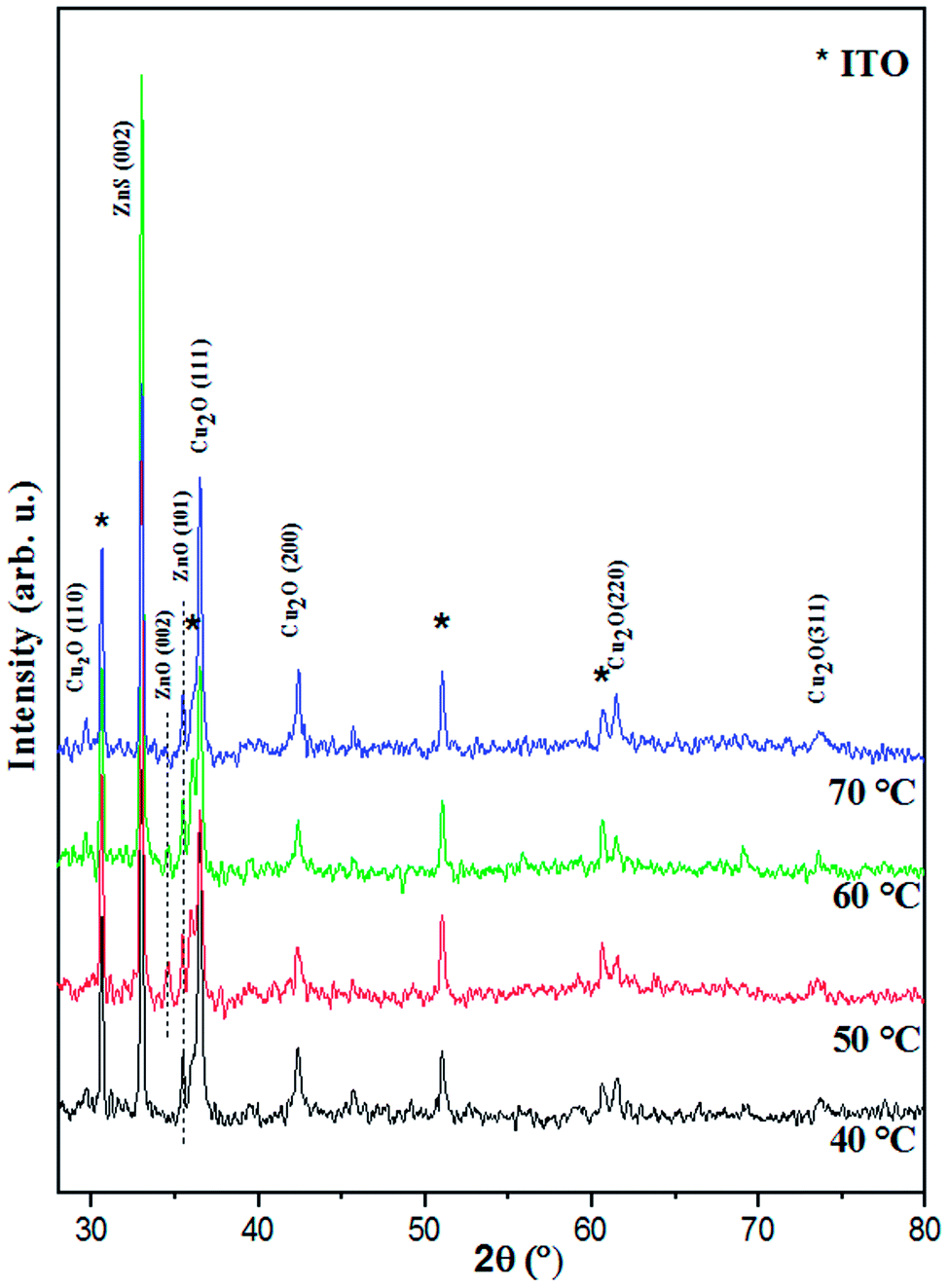 | ||
| Fig. 7 XRD patterns of Cu2O/ZnO/ZnS/ITO heterojunction with different electrodeposition temperatures of ZnS layer. | ||
The crystallites size of the as prepared films have been estimated from the main (111) Bragg peak of cubic Cu2O using:36
 | (4) |
3.6 Optical characterization
The optical properties of our heterojunction are very important for many of their technological applications. The absorbance spectra of ZnO/ZnS/ITO heterostructure and Cu2O/ZnO/ZnS/ITO heterojunctions with different deposited temperatures of ZnS layer were recorded for wavelength range from 300 to 1000 nm as shown in Fig. 8. From the inset of Fig. 8, the ZnO/ZnS/ITO layer shows strong absorption in the UV region extends from 300 to 450 nm. The absorption was significantly improved after the electrodeposition of Cu2O on ZnO/ZnS/ITO layer. As can be seen from Fig. 8, the absorption edge of the Cu2O/ZnO/ZnS/ITO heterojunctions shifted into the visible region (red shift). This amelioration will ensure good performance to the photovoltaic device. Comparing the absorption of the heterojunctions it is clear that Cu2O/ZnO/ZnS/ITO with ZnS layer deposited at 60 °C shows the highest absorbance, which is in accordance with the strong photocurrent generated by this sample under AM 1.5 illumination, as observed in the photoelectrochemical analysis (Fig. 4b).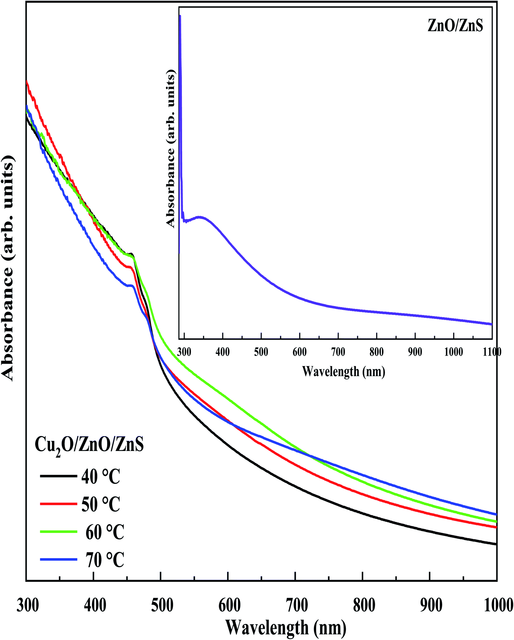 | ||
| Fig. 8 UV-Vis absorption spectra of Cu2O/ZnO/ZnS/ITO heterojunction with different electrodeposition temperatures of ZnS layer. Inset: the UV-Vis absorption spectra of ZnO/ZnS/ITO sample. | ||
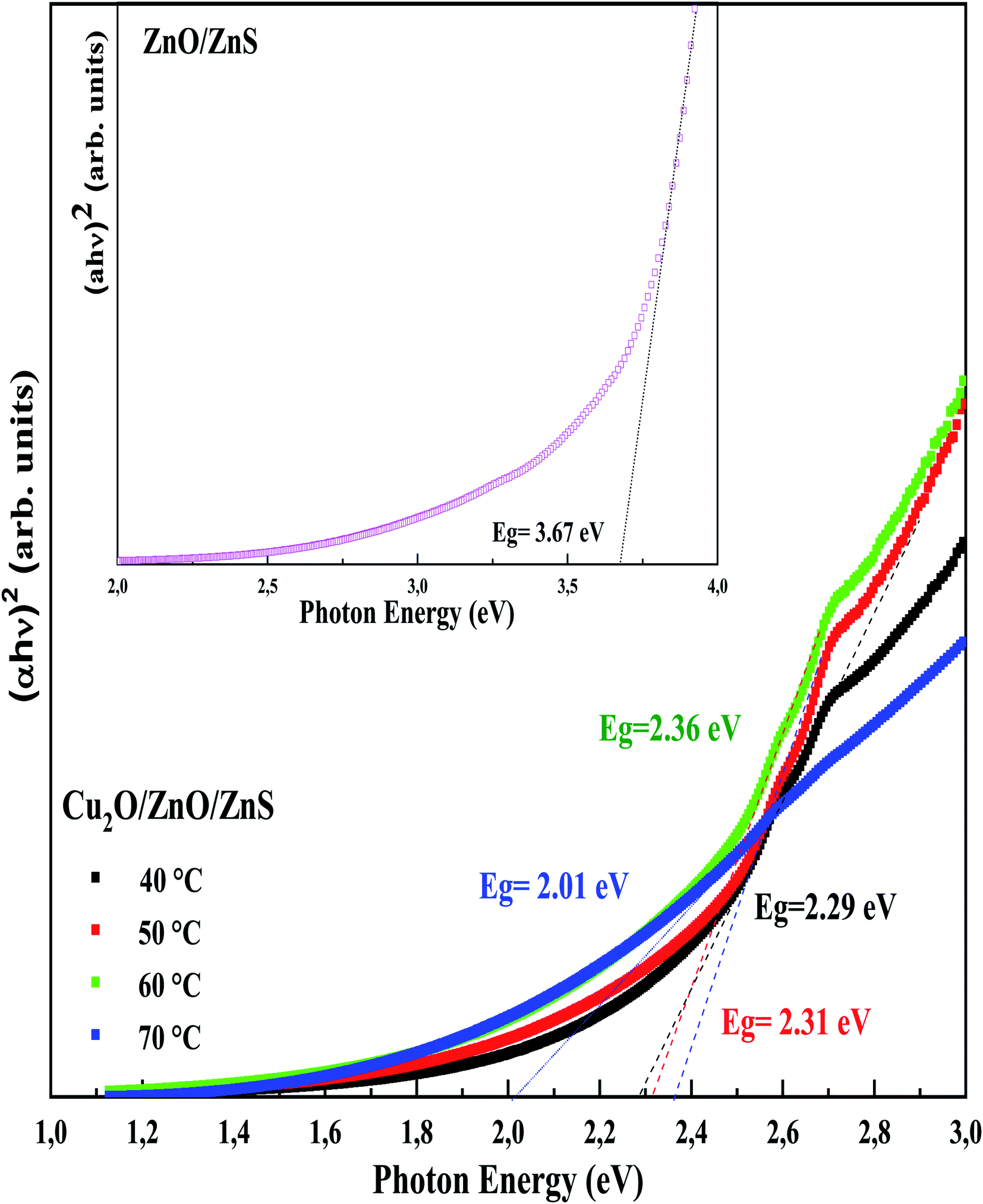
The optical band gap energies can be determined plotting (αhν)2 as a function of photon energy hν using the Tauc relation:38
| (αhν) = A(hν − Eg)n | (5) |
The Tauc plots of ZnO/ZnS/ITO and Cu2O/ZnO/ZnS/ITO heterojunctions are presented in Fig. 9. The band gap obtained for ZnO/ZnS/ITO was 3.67 eV (inset of Fig. 9). Lower band gap energies were determined for Cu2O/ZnO/ZnS/ITO heterojunctions due to the narrow band gap of Cu2O. As can be seen from Fig. 9, the estimated band gap was between 2.01 and 2.36 eV. These values are intermediate, lower than that of ZnS (approximately 3.7 eV) and larger than that of Cu2O (approximately 2.17 eV). The variation of Cu2O/ZnO/ZnS/ITO energy band gap with the deposition temperature of ZnS layer may be explained by the crystallinity deterioration with increasing ZnS deposition temperature.
 | ||
| Fig. 9 Tauc's plot of Cu2O/ZnO/ZnS/ITO heterojunctions with different electrodeposition temperatures of ZnS layer. Inset: Tauc's plot of ZnO/ZnS/ITO sample. | ||
3.7 Current–voltage measurements
The I–V curves of Au/Cu2O/ZnO/ZnS/ITO heterojunctions, with different deposition temperatures of ZnS layer, measured at room temperature in the dark are shown in Fig. 10. This method based on the quantification of the current crossing a junction under the effect of an external electric field. As can be seen from Fig. 10a, Cu2O/ZnO/ZnS/ITO heterojunction with ZnS deposited at 40, 50 and 70 °C shows an excellent ohmic response. However, good rectifying behavior with a low leakage current of 5 × 10⁻⁷ A at a reverse bias of −0.5 V was obtained for the Cu2O/ZnO/ZnS/ITO with ZnS (60 °C), as presented in Fig. 10b, which confirms the formation of p–n junction for this sample. This may be due to the high crystallinity confirmed by XRD.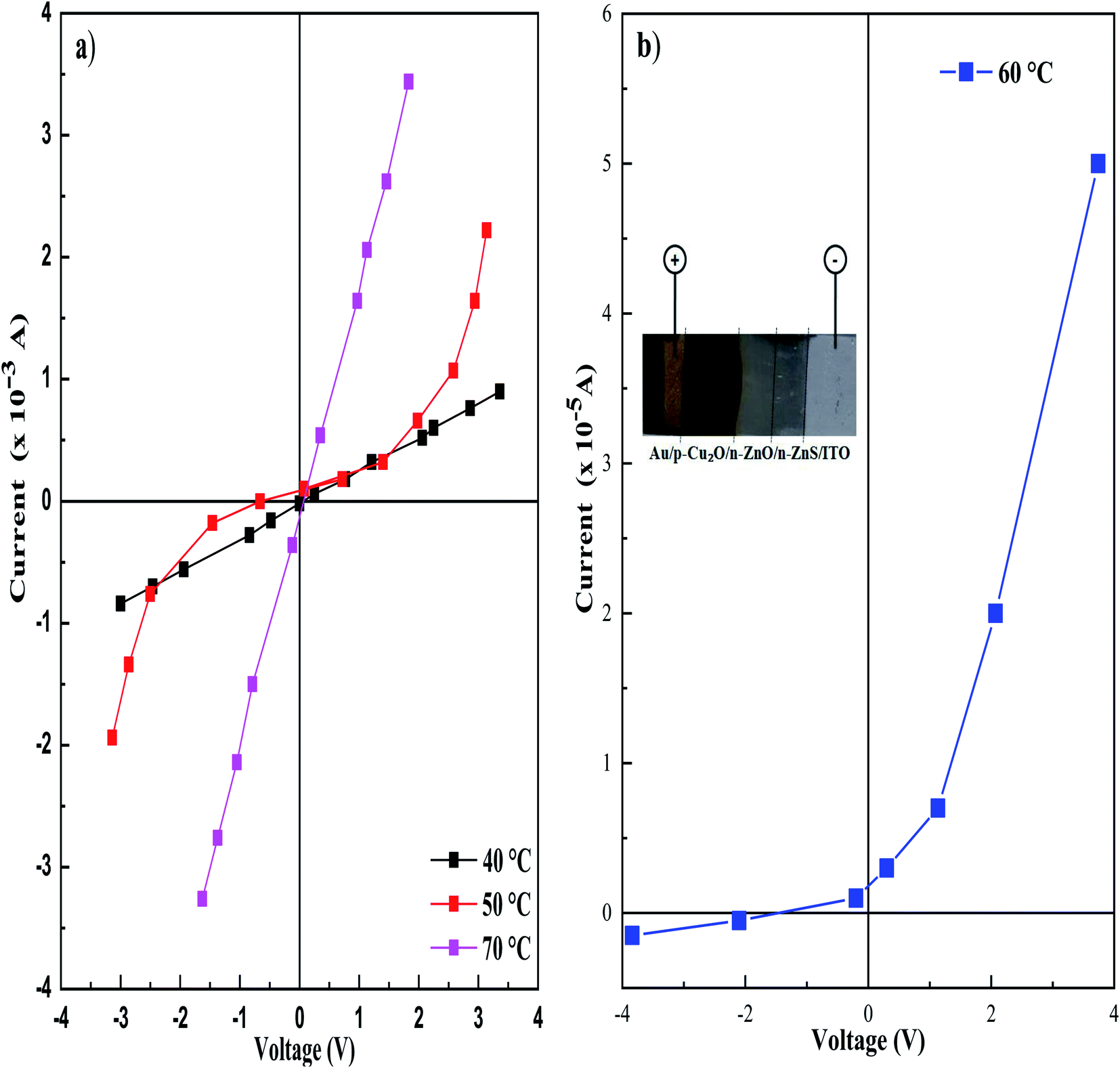 | ||
| Fig. 10 Current–voltage characteristics of Au/p-Cu2O/n-ZnO/n-ZnS/ITO heterojunction in the dark with different electrodeposition temperature of ZnS layer. Inset of (b) photograph of the p-Cu2O/n-ZnO/n-ZnS/ITO heterojunction with Au top contact. | ||
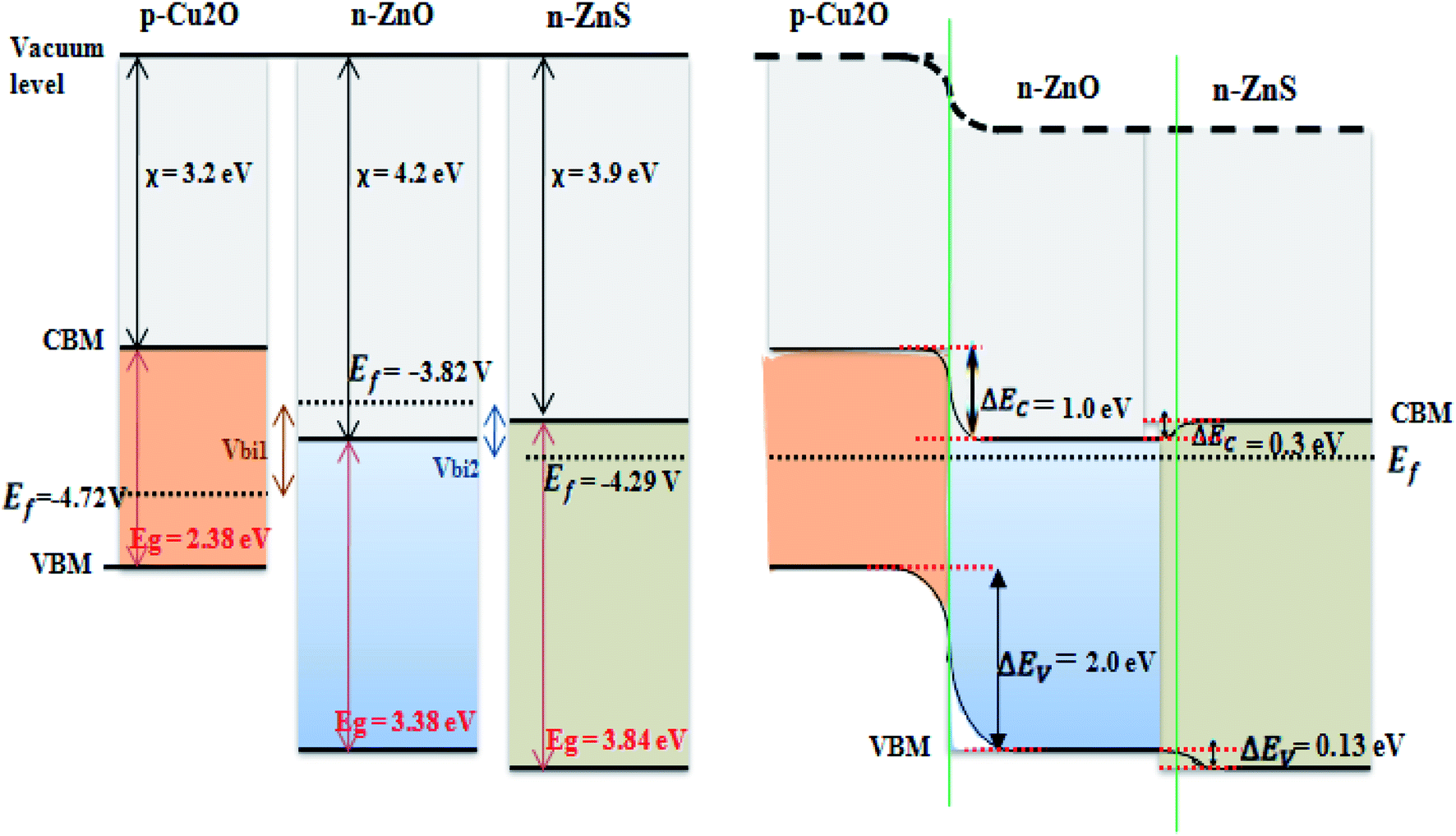
A schematic diagram of the energy-band structure of the p-Cu2O/n-ZnO/n-ZnS heterojunction was constructed simulated using the model proposed by Anderson40 is shown in Fig. 11. When the p- and the n-type semiconductors are in contact, they form a p–n junction with a space-charge region at the interfaces due to the diffusion of electrons and holes driven by the electric field.41 The electrons are transferred to the conduction band of the n-type semiconductors and the holes to the valence band of the p-type semiconductors. The conduction band offset (ΔEC) and the valence band offset (ΔEV) of the heterojunction are represented by the following equations:
| ΔEc = χ1 − | (χ2 6) |
| ΔEv = Eg2 − Eg1 + ΔEc | (7) |
| Efb (in V vs. NHE) = −Ef (in eV vs. vacuum) + VH (in V) − 4.5 | (8) |
| VH (in V) = 0.059(pHPZZP − pH) | (9) |
 | ||
| Fig. 11 Band energy diagram of the isolated states of the n-ZnO, n-ZnS, p-Cu2O and p-Cu2O/n-ZnO/n-ZnS heterojunction under equilibrium condition. | ||
The estimated Fermi level energies for n-ZnS, n-ZnO and p-Cu2O were −4.29, −3.82 eV and −4.72 eV vs. the vacuum, respectively.
Base on the obtained χ, Eg, Ef we proposed an approximate energy-band diagram of the three materials p-type Cu2O, n-type ZnO and n-ZnS before and after the junction formation (Fig. 11). Putting the three materials in contact creates a p–n junction at their interface. The electrons in the n-ZnS layer transferred to the p-Cu2O layer through the n-ZnO layer. In one hand, ZnS has a higher conduction band edge with respect to ZnO, which is advantageous in the injection of excited electrons from ZnS.46 In the other hand, the holes of Cu2O layer transferred in the opposite direction until a constant Fermi-level formed at equilibrium. Hence, creates a built-in electrical potential that can direct the electrons and holes to travel in the opposite direction. The calculated conduction band offset (ΔEC) of the heterojunction Cu2O/ZnO was 1.0 eV, and the valence band offset (ΔEV) was 2.0 eV. The small conduction band offset should result in easy way for electron injection from the n-type ZnO to the p-type Cu2O. In addition, the large valence band offset should result in a thin tunneling barrier across the p–n junction.47
As illustrated in Fig. 11, the built-in potential Vbi1 (−0.9 V) is equal to the difference between the Fermi levels of Cu2O and ZnO. Consequently, the p-Cu2O/n-ZnO/n-ZnS heterojunction, with ZnS deposited at 60 °C, possesses larger built-in potential compared to the other samples. Therefore, p-Cu2O/n-ZnO/n-ZnS (60 °C) got the highest charge separation efficiency, which results in good rectifying behavior in the dark. Moreover, this explains the high photoresponse of this sample reported in the photoelectrochemical analysis (Fig. 4b).
4. Conclusion
In this work, the incorporated n-ZnS layer in p-Cu2O/n-ZnO heterojunction was successfully prepared by electrodeposition on ITO substrate. Where, the deposition temperature of ZnS layer was varied between 40 and 70 °C. It was found that the Cu2O properties were mainly affected by the ZnS deposition temperature. Thus, high crystallinity and large grains were confirmed for the p-Cu2O/n-ZnO/n-ZnS heterojunction with ZnS deposited at 60 °C by XRD analysis and AFM images. In addition, high electron–hole separation efficiency and high photoresponse were confirmed for this sample according to the photoelectrochemical measurements. The UV-Vis spectra show strong absorption in the visible region, which ensures, for this photovoltaic device, a good consumption of the sunlight. The Au/p-Cu2O/n-ZnO/n-ZnS (60 °C)/ITO heterojunction revealed a well-defined electrical rectification characteristic according to the current–voltage (I–V) characteristics. This study demonstrates that electrodeposition, which is easily adapted to other chemical systems, can be a promising technique for large-scale fabrication of low-cost heterojunctions solar cells.Conflicts of interest
There are no conflicts to declare.Acknowledgements
It is included in the PRFU of Ferhat Abbas-Sétif 1 University, Algeria. The authors would like to thank Pr. Attaf Nadhir of Laboratoire Couches Minces et Interfaces, Université des Frères Mentouri-Constantine 1, Algeria for his technical assistance with the electrical measurements.References
- M. Grätzel, J. Photochem and C. Photobiol, Photochem. Rev., 2003, 4, 145–153 CrossRef.
- D. C. Olson, J. Piris, R. T. Collins, S. E. Shaheen and D. S. Ginley, Thin Solid Films, 2006, 496, 26–29 CrossRef CAS.
- M. E. Abu-Zeid, A. E. Rakhshani, A. A. Aljassar and Y. A. Youssef, Phys. Status Solidi A, 1986, 93, 613 CrossRef CAS.
- W. Siripala, L. D. R. D. Perera, K. T. L. De Silva, J. K. D. S. Jayanetti and I. M. Dharmadasa, Sol. Energy Mater. Sol. Cells, 1996, 44, 251–260 CrossRef CAS.
- A. V. Rokade, S. R. Rondiya, A. A. Jadhavar, S. M. Pandharkar, S. D. Karpe, K. D. Diwate and S. R. Jadkar, AIP Conf. Proc., 2016, 1724, 1–7 Search PubMed.
- Y. Hameş and S. E. San, Sol. Energy, 2004, 77, 291–294 CrossRef.
- C. J. Dong, W. X. Yu, M. Xu, J. J. Cao, C. Chen, W. W. Yu and Y. D. Wang, J. Appl. Phys., 2011, 110, 073712 CrossRef.
- Y. Levskaya, R. L. Z. Hoye, A. Sadhanala, K. P. Musselman and J. L. MacManus-Driscoll, Sol. Energy Mater. Sol. Cells, 2015, 135, 43–48 CrossRef.
- T. Minami, Y. Nishi and T. Miyata, Appl. Phys. Express, 2016, 9, 052301 CrossRef.
- F. M. A. Hernández, M. C. López, V. Donderis, M. González, B. Mar and J. R. Ramos-Barrad, Thin Solid Films, 2008, 516, 1622–1625 CrossRef.
- S. M. Al-Hilli, R. T. Al-Mofarji, P. Klason, M. Willander, N. Gutman and A. J. Sa'ar, J. Appl. Phys., 2008, 103, 014302 CrossRef.
- M. Sookhakian, Y. M. Amin, W. J. Basirun, M. T. Tajabadi and N. Kamarulzaman, J. Lumin., 2014, 145, 244–252 CrossRef CAS.
- H. A. Cheol, Y. K. Young, C. K. Dong, K. M. Sanjay and K. C. Hyung, J. Appl. Phys., 2009, 105, 013502 CrossRef.
- F. Xiaosheng, Z. Tianyou, K. G. Ujjal, L. Liang, W. Limin, B. Yoshio and G. Dmitri, Prog. Mater. Sci., 2011, 56, 175–287 CrossRef.
- Ü. Neslihan and A. M. Çetin, J. Mater. Sci.: Mater. Electron., 2010, 34, 287–292 Search PubMed.
- J. Jan, X. Fan, L. Zhang, Y. Bando, U. K. Gautam, B. Dierre, T. Sekiguchi and D. Goldberg, Nano Lett., 2008, 8, 2794–2799 CrossRef PubMed.
- W. Zhiqiang, L. Xuedong, G. Jiangfeng, H. Hongbo, G. Shulin and Y. Shaoguang, Cryst. Growth Des., 2008, 8, 3911–3913 CrossRef.
- M. W. Murphy, X. T. Zhou, J. Y. P. Ko, J. G. Zhou, F. Heigl and T. K. Sham, J. Chem. Phys., 2009, 130, 084707 CrossRef CAS PubMed.
- S. Simmi and C. Santa, Electron. Mater. Lett., 2013, 9, 267–271 CrossRef.
- J. Schrier, D. O. Demchenko and L. W. Wang, Nano Lett., 2007, 7, 2377–2382 CrossRef CAS PubMed.
- L. Mentar, O. Baka, M. R. Khelladi, A. Azizi, S. Velumani, G. Schmerber and A. Dinia, J. Mater. Sci.: Mater. Electron., 2015, 26, 1217–1224 CrossRef CAS.
- S. Laidoudi, A. Y. Bioud, A. Azizi, G. Schmerber, J. Bartringer, S. Barre and A. Dinia, Semicond. Sci. Technol., 2013, 28, 115005–115011 CrossRef.
- Y. F. Cheng, C. Yang and J. L. Luo, Thin Solid Films, 2002, 416, 169–173 CrossRef CAS.
- A. W. Bott, Electrochemistry of semiconductors, Curr. Sep., 1998, 17, 87–91 CAS.
- H. Noh, M. Scharrer, M. A. Anderson, R. P. H. Chang and H. Cao, Phys. Rev. B: Condens. Matter Mater. Phys., 2008, 77, 115136 CrossRef.
- Z. Zhang and P. Wang, J. Mater. Chem., 2012, 22, 2456–2464 RSC.
- C. M. McShane and K.-S. Choi, J. Phys. Chem., 2012, 14, 6112 CAS.
- F. Caballero-Briones, J. M. Artes, I. Diez-Perez, P. Gorostiza and F. Sanz, J. Phys. Chem. C, 2009, 113, 1028 CrossRef CAS.
- C. Yilmaz and U. Unal, Appl. Surf. Sci., 2016, 368, 456–463 CrossRef CAS.
- R. Ghosh, D. Basak and S. Fujihara, J. Appl. Phys., 2004, 96, 2689–2692 CrossRef CAS.
- Y. Yang, J. Han, X. Ning, W. Cao, W. Xu and L. Guo, ACS Appl. Mater. Interfaces, 2014, 6, 22534–22543 CrossRef CAS PubMed.
- Z. Kang, X. Yan, Y. Wang, Z. Bai, Y. Liu, Z. Zhang, P. Lin, X. Zhang, H. Yuan, X. Zhang and Y. Zhang, Sci. Rep., 2015, 5, 78–82 Search PubMed.
- Z. Bai and Y. Zhang, J. Alloys Compd., 2017, 698, 133–140 CrossRef CAS.
- R. Kern, R. Sastrawan, J. Ferber, R. Stangl and J. Luther, Electrochim. Acta, 2002, 47, 4213–4225 CrossRef CAS.
- M. Guo, K. Xie, J. Lin, Z. Yong, C. T. Yip, L. Zhou, Y. Wang and H. Huang, Energy Environ. Sci., 2012, 5, 9881–9888 RSC.
- B. D. Cullity, Elements of X-ray Diffraction, Addison Wesley, Reading, MA, 2nd edn, 1978 Search PubMed.
- D. K. Zhang, Y. C. Liu, Y. L. Liu and H. Yang, Phys. B, 2004, 351, 178 CrossRef CAS.
- H. Lahmar, A. Azizi, G. Schmerber and A. Dinia, RSC Adv., 2016, 6, 68663–68674 RSC.
- J. Tauc, in Optical properties of solids, ed. F. Abeles, North-Holland Pub Co., Amsterdam, vol. 22, 1970 Search PubMed.
- A. G. Milnes and D. L. Feucht, Heterojunctions and Metal-Semiconductor Junctions, Academic Press, New-York, 1972 Search PubMed.
- L. Jiang, G. Zhou, J. Mi and Z. Wu, Catal. Commun., 2012, 24, 48–51 CrossRef CAS.
- R. K. Swank, Phys. Rev., 1967, 153, 844 CrossRef CAS.
- W. Siripala, A. Ivanovskaya, T. F. Jaramillo, S. H. Baeck and E. W. McFarland, Sol. Energy Mater. Sol. Cells, 2003, 77, 229–237 CrossRef CAS.
- H. Kobayashi, H. Mori, T. Ishida and Y. Nakato, J. Appl. Phys., 1995, 77, 1301–1307 CrossRef CAS.
- Y. Xu and M. A. A. Schoonen, Am. Mineral., 2000, 85, 543–5565 CrossRef CAS.
- L. P. Wu, Y. L. Zhang, L. Z. Long, C. P. Cen and X. J. Li, RSC Adv., 2014, 4, 20716–20721 RSC.
- T. J. Hsueh, C. L. Hsu, S. J. Chang, P. W. Guo, J. H. Hsieh and I. C. Chen, Scr. Mater., 2007, 57, 53–56 CrossRef CAS.
| This journal is © The Royal Society of Chemistry 2019 |