
 Open Access Article
 This Open Access Article is licensed under a Creative Commons Attribution-Non Commercial 3.0 Unported Licence
A silicon-based quantum dot random laser
Zhiyang Xu,
Hao Zhang,
Chao Chen,
Gohar Aziz,
Jie Zhang,
Xiaoxia Zhang,
Jinxiang Deng*,
Tianrui Zhai * and
Xinping Zhang
* and
Xinping Zhang
Institute of Information Photonics Technology, College of Applied Sciences, Beijing University of Technology, Beijing 100124, China. E-mail: jdeng@bjut.edu.cn; trzhai@bjut.edu.cn
First published on 11th September 2019
Abstract
Herein, a quantum dot random laser was achieved using a silicon nanowire array. The silicon nanowire array was grown by a metal-assisted chemical etching method. A colloidal quantum dot solution was spin-coated on silicon nanowires to form the random laser. The performance of the random laser was controlled by the resistivity of silicon wafers and the length of silicon nanowires. A transition from incoherent random lasing to coherent random lasing was obtained by increasing the resistivity of the silicon wafers. The random lasing threshold increased with an increase in the length of the silicon nanowires. These results may be useful to explore high-performance silicon-based random lasers.
1. Introduction
Over the past few decades, silicon (Si) has continued to be the material of choice for robust applications due to its abundance in nature and the existence of well-developed techniques e.g. solar cells, computer chips and sensors.1,2 However, since bulk Si is an indirect semiconductor with a low electron–hole recombination efficiency and shows very inefficient light emission, the fabrication of efficient Si-based light-emitting devices remains a big challenge.3 Nanostructured Si, in particular, Si nanowires (NWs), has attracted significant attention due to its unique physical characteristics and diverse range of applications such as in nanoelectronics, optoelectronics, thermoelectrics, photovoltaics, energy storage, and sensors.4–6 Recently, the metal-assisted chemical etching (MACE) method has emerged as a promising and significant tool for the effective production of large-area, aligned and well-controlled Si NWs.7 The Si NWs fabricated by the MACE method have attracted broad attention due to their fantastic properties and potential applications.8–12 During the MACE process, the length of the Si NWs increases with an increase in the etching time. Moreover, a mesoporous structure is formed on the NW side walls due to crystal defects and impurities, such as dopants, in the p-type Si. Hence, Si wafers with lower resistivity can lead to higher mesopores.13 These high-aspect ratio Si NWs decorated with arbitrary shaped mesopores have been applied as a fabrication platform for different materials such as ZnO nanocrystals, Pd nanoparticles, Au NWs, and perovskite nanoparticles. The devices constructed by these compounds can be employed in different fields such as sensing, photocatalysis, and light emission.14–17Ever since random lasers have been theoretically proposed by V. S. Letokhov,18 they have attracted significant attention due to their appealing physical properties and potential applications over the past few years.19–21 Due to the absence of a resonance cavity with reflection mirrors, the major advantage of random lasers over regular lasers is that their production is cheap, and the required technology is relatively simple.22 Furthermore, a particular advantage of the random lasers is that they can be produced with small sizes and achieve low spatial coherence.23,24 Recently, random lasers have been fabricated by doping various gain media, such as laser dyes, perovskites, and quantum dots, into arbitrary composited micro/nano-structures based on multiple scattering that can achieve random laser output on the fabrication platform for different materials.25–32 However, the influence of a Si NW array on the performance of a random laser has not been explored systematically.
In this study, we investigated a quantum dot random laser based on the Si NW array grown by the MACE method. The random laser was fabricated by spin-coating the colloidal quantum dot solution on the fabrication platforms of the Si NW arrays with different resistivities. Random lasing was observed when the device was optically pumped. The characteristic of random lasing can be modified by changing the parameters of the Si NWs. Random lasing transformed from incoherent to coherent when the resistivity of boron-doped p-type Si wafers was varied from 1–10 Ω cm to 0.1–0.01 Ω cm. Moreover, as the length of the Si NWs increased, the threshold of the random laser became higher.
2. Experimental details
The Si NWs were grown by the MACE process using Si wafers at room temperature.8 The boron-doped p-type Si (100) wafers with different resistivities (ρ), i.e. 1–10 Ω cm and 0.01–0.1 Ω cm, were used in the experiment. Initially, the Si wafers were obtained by cleaving the boron-doped p-type Si (100) wafers into 1.5 × 1.5 cm2 pieces. Then, the Si pieces were cleaned using acetone and ethanol under the ultrasonic condition for 5 min to remove the organic impurities on the Si surface. The samples were rinsed with deionized water in each step. Finally, the cleaned wafers were dried under a N2 flow.After the cleaning process, a two-step MACE process was used, consisting of the deposition of a Ag catalyst on the Si surface in a solution to form AgNO3–HF and etching in the HF–H2O2 solution, as shown schematically in Fig. 1. The Si wafers were first immersed in a solution containing 4.8 M HF and 0.004 M AgNO3 for 1 min to deposit the Ag nanoparticles (Ag NPs) on the Si wafers, as shown in Fig. 1(a). Subsequently, the Ag NP-coated Si samples were etched in a solution containing 4.8 M HF and 0.04 M H2O2 for different time durations to form the Si NW arrays, as illustrated in Fig. 1(b). Next, a solution of the colloidal quantum dots (core/shell/shell CdSe/CdS/ZnS) at the concentration of 0.03 g mL−1 was spin coated onto the Si NW substrates at the speed of 1000 rpm. The band gap energy of CdSe is 1.76 eV, which is responsible for lasing.33 The random laser devices based on the Si NWs were fabricated as illustrated in Fig. 1(c).
 | ||
| Fig. 1 Fabrication procedure of the Si-based quantum dot random laser device. (a) Ag NPs are deposited on the Si surface in an aqueous solution containing AgNO3 and HF. (b) Ag NPs catalyze the etching of the Si substrate in a solution composed of HF, H2O2, and H2O. (c) Colloidal quantum dots are spin-coated onto the Si NW substrates. | ||
During the experiment, the top-view and cross-sectional view of the etched Si NWs substrates were characterized by scanning electron microscopy (SEM, Hitachi S-4800). A non-polarized white light from a tungsten halogen lamp (HL-2000) was employed to characterize the PL spectra. The laser devices were optically pumped by a femtosecond laser. The laser emission was collected by an optical fiber coupled to a spectrometer (Maya 2000 Pro, Ocean Optics).
3. Results and discussion
3.1 Mechanism of action and morphology of the Si NW array
During the etching process, the equation of the chemical reaction was as follows:| Si + 4Ag+ + 6F− → 4Ag + SiF62− | (1) |
| Ag+ + e → Ag | (2) |
| 2Ag + H2O2 + 2H+ → 2Ag+ + 2H2O | (3) |
| Si + H2O2 + 6F− + 4H+ → SiF62− + 4H2O | (4) |
At first, there was an oxidation–reduction reaction between silicon and silver ions in the mixture of AgNO3 and HF. Si was oxidized, and Ag NPs were formed on the surface of the Si wafers. The formed silicon oxide was dissolved in the HF solution, as shown in eqn (1) and (2). Then, the samples covered with the Ag NPs were immersed in a solution of HF and H2O2. Due to the strong oxidizing property of the H2O2 solution, the Ag NPs were oxidized immediately and dissolved in the solution. As the Ag NPs worked as a catalyst in the reaction, H2O2 preferably formed H2O near the surface of the Ag NPs, as shown in eqn (3). After this, the Ag+ ion produced by H2O2 diffused into the interface between silicon and Ag nanoparticles. Then, silicon was oxidized into silicon oxide, and silicon oxide was removed by HF again, as illustrated in eqn (4). Finally, with the progress of the reaction, the Ag NPs gradually etched down, and the Si NWs arrays were formed.
Boron-doped p-type Si (100) wafers with the different resistivities (ρ) of 1–10 Ω cm (sample A) and 0.01–0.1 Ω cm (sample B) were used in the experiment. However, the etching rate of the sample B was lower than that of the sample A because the impurities in wafer did not participate in the etching reaction.34 To fabricate the Si NW arrays of same length, the concentration of the etching solution was kept constant, whereas the etching times of the Si wafer with high resistivity and the Si wafer with low resistivity were different. A list of the key parameters and lengths of the resulting nanowires is summarized in Table 1.
| Resistivity | Length of nanowires | ||||
|---|---|---|---|---|---|
| 300 nm | 400 nm | 600 nm | 800 nm | 1000 nm | |
| a The concentrations of H2O2 and HF were kept at 0.4 M and 4.8 M, respectively. | |||||
| (ρ) 1–10 Ω cm | 3 min | 4 min | 5 min | 6 min | 7 min |
| (ρ) 0.01–0.1 Ω cm | 4 min | 5.5 min | 7 min | 8.5 min | 10 min |
Fig. 2 shows the top-view SEM and the cross-sectional view SEM images of the Si NWs acquired from the sample A and sample B with the etching time of 7 min. In Fig. 2(a) and (b), the top-view SEM images of the Si NW array revealed that the resistivity affected the surface morphology of the Si NW array. The diameter of the pores decreased, and the density of the Si NW array increased with the increasing resistivity of the starting Si wafer in the etchant. This can be attributed to the doping density of the Si wafer. The cross-sectional SEM images demonstrated the vertically aligned Si NW arrays with the lengths of 1000 nm and 600 nm, as shown in Fig. 2(c) and (d), respectively.
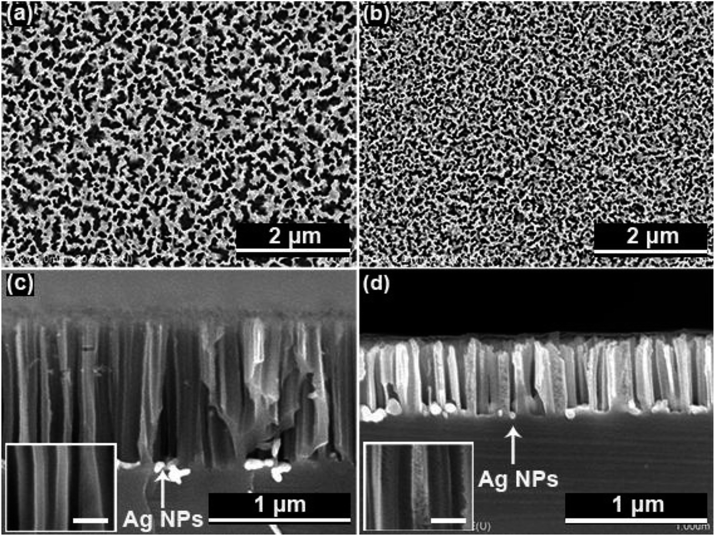 | ||
| Fig. 2 (a) and (b) SEM images of the top view of the sample A and sample B, respectively. The etching time is 7 min. (c) and (d) Cross-sectional view of the sample A and sample B, respectively. The Ag NPs are indicated by arrows. The insets show the magnified view of the Si NW array. The scale bar in the inset is 100 nm. | ||
The etching rate of the sample B was lower than that of the sample A, due to which the impurity in the wafer did not participate in the etching reaction. There remained Ag NPs at the roots of the nanowires. Note that arbitrary shaped mesopores were decorated on the Si NWs with low resistivity; on the other hand, the Si NWs with high resistivity were nonporous with smooth surfaces, as shown in the insets of Fig. 2(c) and (d). The mesoporous structure may enhance the scattering effect.
3.2 Spectral characteristics of the random laser
The random laser device was fabricated by coating the prepared quantum dot solutions as efficient gain materials on the fabrication platforms of the sample A and sample B. The lengths of both the sample A and the sample B were 300 nm. The disordered Si NWs were generally beneficial for the random laser system. They increased the scattering of photons generated in the gain materials as well as the dwell time or path length. Random lasing occurred when the device was pumped optically due to the enhancement of the Si NW array. A femtosecond laser beam (200 fs) with the wavelength of 400 nm and the repetition frequency of 1 kHz was employed as the pump source. The diameter of the laser spot was about 3 mm. The pump beam impinged on the random laser with an incident angle (∼30 degree) to simplify the actual test. The intensity of the laser beam could be tuned continuously using a variable optical attenuator. The laser emission was collected by a fiber lens onto an optical fiber that was coupled to a spectrometer.Fig. 3(a) and (c) show the output intensity of the quantum dot random laser based on the sample A and the sample B with different pulse pumping energies, respectively. At low pumping energy, the emission spectrum was broad. The broad emission spectrum began to narrow down when the pumping energy exceeded the laser threshold. For the sample A, an emission peak can be observed at ∼640 nm, and the full width at half maximum (FWHM) of the emission peak is about 8 nm; on the other hand, the emission peak of the sample B appears at ∼640 nm, and the FWHM is about 10 nm. The inset shows the enlarged view of the emission peak. The blue curve indicates the PL spectra of the quantum dots coated on the bulk Si. The FWHM of the PL emission peaks is about 30 nm.
 | ||
| Fig. 3 (a) Measured spectra of random lasing on the sample A. (b) Output intensity and linewidth of the laser as a function of the pumping energy. (c) Measured spectra of random lasing on the sample B. (d) Output intensity and linewidth of the laser as a function of the pumping energy. The insets show the enlarged view of the emission peak indicated by the black circle. The black arrows indicate the laser threshold. | ||
Fig. 3(b) and (d) present the plots of emission intensity and FWHM as a function of pumping energy for the sample A and the sample B, respectively. It can be clearly observed that there is a non-linear variation between the intensity FWHM and pumping energy. The threshold for the sample A and the sample B is around 423 μJ cm−2 and 325 μJ cm−2, respectively. Moreover, the FWHM for the sample A (the sample B) rapidly narrowed down to 8 nm (10 nm) from 30 nm over the threshold, which was a signature for the occurrence of random lasing.
Different spectral characteristics can be observed between the sample A and the sample B. In the case of the sample B, there are lasing spikes above the main peak, whereas there is one lasing peak in the case of the sample A. On the other hand, the threshold of the sample B is lower than that of the sample A. This can be attributed to the surface morphology of the Si NW array. In the high-resistivity sample A, the Si NW array density is small, and the pore diameters are large. The scattering effect is very weak such that the conditions forming Anderson localization cannot be satisfied to obtain a coherent random laser. However, the low-resistivity sample B with a strong scattering effect showed better performance than the high-resistivity sample A due to its low threshold and more lasing modes.
To investigate the influence of the Si NW length on the random laser performance, a control experiment was performed. In the experiment, the sample B was used due to its better performance. The sample B was etched for different time durations with a constant concentration of the etching solution and then coated with the colloidal quantum dots to form a laser device.
Fig. 4(a)–(d) show the cross-sectional SEM images of the nanowires with the lengths of 300 nm, 400 nm, 600 nm and 800 nm, which were fabricated by etching the sample B for 4, 5.5, 7, and 8.5 min, respectively. The growth rate of the Si NWs was ∼130 nm min−1. The Si NW length increased linearly with the etching time duration. Fig. 4(e) presents the threshold of the output laser as a function of the length of the Si NWs on the random laser device. It can be observed that the laser threshold increases from 325 μJ cm−2 to 1150 μJ cm−2 with an increase in the Si NW length; this can be attributed to the additional loss caused by the longer Si NWs. Some radiation of the quantum dots leaked into the Si NW array and was trapped by the layer of the Si NW arrays, forming a scattering loss channel.
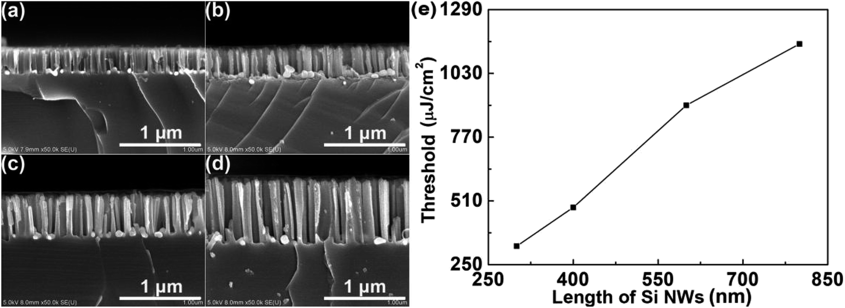 | ||
| Fig. 4 (a), (b), (c) and (d) SEM images of the cross-sectional view for the sample B with the lengths of 300 nm, 400 nm, 600 nm and 800 nm, respectively. (e) The threshold of the random laser as a function of the length of Si NWs. | ||
4. Conclusions
In conclusion, we demonstrated a Si-based random laser device, which was fabricated by the compound structure of the MACE method-grown Si NWs and colloidal quantum dots. The characteristic of random lasing could be controlled by controlling the surface morphology of the Si NW arrays and the length of the Si NWs. Random lasing transition transformed from incoherent to coherent by changing the resistivity of the boron-doped p-type Si wafers. The threshold of the random lasing increased with an increase in the length of the Si NWs due to the introduction of the additional loss channel. These results can be utilized in the future applications of Si-based random lasers.Conflicts of interest
There are no conflicts to declare.Acknowledgements
The authors gratefully acknowledge the financial support of the National Natural Science Foundation of China (NSFC) (61822501, 11574015) and Beijing Natural Science Foundation (Z180015, 4192016).References
- K. Lord, B. Yan, J. Yang and S. Guha, Light-induced increase in the open-circuit voltage of thin-film heterogeneous silicon solar cells, Appl. Phys. Lett., 2001, 79, 3800–3802 CrossRef CAS.
- S. Y. Cho, S. W. Seo, M. A. Brooke and N. M. Jokerst, Integrated detectors for embedded optical interconnections on electrical boards, modules, and integrated circuits, IEEE J. Sel. Top. Quantum Electron., 2002, 8, 1427–1434 CrossRef CAS.
- T. Takagahara and K. Takeda, Theory of the quantum confinement effect on excitons in quantum dots of indirect-gap materials, Phys. Rev. B: Condens. Matter Mater. Phys., 1992, 46, 15578–15581 CrossRef CAS PubMed.
- B. Tian, X. Zheng, T. J. Kempa, Y. Fang, N. Yu, G. Yu, J. Huang and C. M. Lieber, Coaxial silicon nanowires as solar cells and nanoelectronic power sources, Nature, 2007, 449, 885–889 CrossRef CAS PubMed.
- R. Yan, D. Gargas and P. Yang, Nanowire photonics, Nat. Photonics, 2009, 3, 569–576 CrossRef CAS.
- K. Q. Peng and S. T. Lee, Silicon nanowires for photovoltaic solar energy conversion, Adv. Mater., 2011, 23, 198–215 CrossRef CAS.
- X. Li and P. W. Bohn, Metal-assisted chemical etching in HF/H2O2 produces porous silicon, Appl. Phys. Lett., 2000, 77, 2572–2574 CrossRef CAS.
- K. Q. Peng, Y. J. Yan, S. P. Gao and J. Zhu, Synthesis of large-area silicon nanowire array via self-assembling nanoelectrochemistry, Adv. Mater., 2002, 14, 1164–1167 CrossRef CAS.
- Z. Huang, N. Geyer, P. Werner, J. de Boor and U. Gösele, Metal-assisted chemical etching of silicon: a review, Adv. Mater., 2011, 23, 285–308 CrossRef CAS.
- R. Ghosh and P. K. Giri, Silicon nanowire heterostructures for advanced energy and environmental applications: a review, Nanotechnology, 2017, 28, 012001 CrossRef.
- R. Ghosh, P. K. Giri, K. Imakita and M. Fujii, Origin of visible and near-infrared photoluminescence from chemically etched Si nanowires decorated with arbitrarily shaped Si nanocrystals, Nanotechnology, 2014, 25, 045703 CrossRef.
- R. Ghosh, J. Ghosh, R. Das, L. P. L. Mawlong, K. K. Paul and P. K. Giri, Multifunctional Ag nanoparticle decorated Si nanowires for sensing, photocatalysis and light emission applications, J. Colloid Interface Sci., 2018, 532, 464–473 CrossRef CAS.
- Y. Qu, H. Zhou and X. Duan, Porous silicon nanowires, Nanoscale, 2011, 3, 4060–4068 RSC.
- R. Ghosh, P. K. Giri, K. Imakita and M. Fuji, Photoluminescence signature of resonant energy transfer in ZnO coated Si nanocrystals decorated on vertical Si nanowires array, J. Alloys Compd., 2015, 638, 419–428 CrossRef CAS.
- X. H. Sun, N. B. Wong, C. P. Li, S. T. Lee, P. S. G. Kim and T. K. Sham, Reductive self-assembling of Pd and Rh nanoparticles on silicon nanowire templates, Chem. Mater., 2004, 16, 1143–1152 CrossRef CAS.
- T. C. Wong, C. P. Li, R. Q. Zhang and S. T. Lee, Gold nanowires from silicon nanowire templates, Appl. Phys. Lett., 2004, 84, 407–409 CrossRef CAS.
- R. Ghosh, J. Ghosh and P. K. Giri, Mesoporous Si nanowire templated controlled fabrication of organo-metal halide perovskite nanoparticles with high photoluminescence quantum yield for light emitting applications, ACS Appl. Nano Mater., 2018, 1, 1551–1562 CrossRef.
- V. S. Letokhov, Generation of light by a scattering medium with negative resonance absorption, J. Exp. Theor. Phys., 1968, 26, 835–840 Search PubMed.
- N. M. Lawandy, R. M. Balachandran, A. S. L. Gomes and E. Sauvain, Laser action in strongly scattering media, Nature, 1994, 368, 436–438 CrossRef.
- H. Cao, Review on latest developments in random lasers with coherent feedback, J. Phys. A: Math. Gen., 2005, 38, 10497–10535 CrossRef CAS.
- D. S. Wiersma, The physics and applications of random lasers, Nat. Phys., 2008, 4, 359–367 Search PubMed.
- R. C. Polson and Z. V. Vardeny, Random lasing in human tissues, Appl. Phys. Lett., 2004, 85, 1289–1291 CrossRef CAS.
- B. Redding, M. A. Choma and H. Cao, Speckle-free laser imaging using random laser illumination, Nat. Photonics, 2012, 6, 355–359 CrossRef CAS.
- D. S. Wiersma, The smallest random laser, Nature, 2000, 406, 132–133 CrossRef CAS.
- T. Zhai, J. Chen, L. Chen, J. Wang, D. Liu, S. Li, H. Liu and X. Zhang, A plasmonic random laser tunable through stretching silver nanowires embedded in a flexible substrate, Nanoscale, 2015, 7, 2235–2240 RSC.
- T. Zhai, Z. Xu, X. Wu, Y. Wang, F. Liu and X. Zhang, Ultra-thin plasmonic random lasers, Opt. Express, 2016, 24, 437–442 CrossRef CAS.
- T. Zhai, X. Zhang, Z. Pang, X. Su, H. Liu, S. Feng and L. Wang, Random laser based on waveguided plasmonic gain channels, Nano Lett., 2011, 11, 1374–1378 CrossRef.
- Y. Chen, J. Herrnsdorf, B. Guilhabert, Y. Zhang, I. M. Watson, E. Gu, N. Laurand and M. D. Dawson, Colloidal quantum dot random laser, Opt. Express, 2011, 19, 2996–3003 CrossRef CAS.
- M. Hutchings, I. O'Driscoll, P. M. Smowton and P. Blood, Fermi-dirac and random carrier distributions in quantum dot lasers, Appl. Phys. Lett., 2014, 104, 031103 CrossRef.
- A. K. Augustine, P. Radhakrishnan, V. P. N. Nampoori and M. Kailasnath, Enhanced random lasing from a colloidal CdSe quantum dot-Rh6G system, Laser Phys. Lett., 2015, 12, 025006 CrossRef.
- W. Lina, Y. Liao, H. Lin and Y. Chen, All-marine based random lasers, Org. Electron., 2018, 62, 209–215 CrossRef.
- J. Xia, K. Xie, J. Ma, X. Chen, Y. Li, J. Wen, J. Chen, J. Zhang, S. Wu, X. Cheng and Z. Hu, The transition from incoherent to coherent random laser in defect waveguide based on organic/inorganic hybrid laser dye, Nanophotonics, 2018, 7, 1341–1350 CAS.
- D. V. Talapin, I. Mekis, S. Götzinger, A. Kornowski, O. Benson and H. Weller, CdSe/CdS/ZnS and CdSe/ZnSe/ZnS core–shell–shell nanocrystals, J. Phys. Chem. B, 2004, 108, 18826 CrossRef CAS.
- X. Zhong, Y. Qu, Y. C. Lin, L. Liao and X. Duan, Unveiling the formation pathway of single crystalline porous silicon nanowires, ACS Appl. Mater. Interfaces, 2011, 3, 261–270 CrossRef CAS.
| This journal is © The Royal Society of Chemistry 2019 |