
 Open Access Article
 This Open Access Article is licensed under a Creative Commons Attribution-Non Commercial 3.0 Unported Licence
Metastable monoclinic [110] layered perovskite Dy2Ti2O7 thin films for ferroelectric applications
D. Pravarthana *ab,
O. I. Lebedevb,
A. Davidb,
A. Fouchetb,
M. Trassinc,
G. S. Rohrerd,
P. A. Salvadord and
W. Prellier*b
*ab,
O. I. Lebedevb,
A. Davidb,
A. Fouchetb,
M. Trassinc,
G. S. Rohrerd,
P. A. Salvadord and
W. Prellier*b
aCAS Key Laboratory of Magnetic Materials and Devices, Ningbo Institute of Materials Technology and Engineering, Chinese Academy of Sciences, Ningbo 315201, People's Republic of China. E-mail: dpravarthana@gmail.com
bLaboratoire CRISMAT, CNRS UMR 6508, ENSICAEN, Normandie Université, 6 Bd Maréchal Juin, F-14050 Caen Cedex 4, France. E-mail: wilfrid.prellier@ensicaen.fr
cDepartment of Materials, ETH Zurich, Vladimir-Prelog-Weg 4, 8093 Zurich, Switzerland
dDepartment of Materials Science and Engineering, Carnegie Mellon University, 5000 Forbes Avenue, Pittsburgh, Pennsylvania 15213, USA
First published on 25th June 2019
Abstract
Using the Combinatorial Substrate Epitaxy (CSE) approach, we report the stabilization of Dy2Ti2O7 epitaxial monoclinic, layered-perovskite phase Dy2Ti2O7 thin films. To achieve this, the films are deposited on high density, polished La2Ti2O7 polycrystalline ceramic substrates, which are stable as monoclinic layered-perovskites, and were prepared by conventional sintering. Microstructural analysis using electron backscatter diffraction (EBSD), electron diffraction (ED), and high-resolution transmission electron microscopy (HRTEM) support this observation. Further, they reveal that the cubic pyrochlore phase is observed far from the interface as films are grown thicker (100 nm), confirming the importance of substrate-induced phase and space group selection. This works reinforces the vast potential of CSE to promote the stabilization of metastable phases, thus giving access to new functional oxide materials, across a range of novel material systems including ferroelectrics.
1. Introduction
The recent progress in epitaxial metal oxide growth towards artificial micro/nano structures, metastable phase stabilization, and nanocomposite design has been triggering interest due to the wide range of oxide functional properties, such as ferroelectricity, high-TC superconductivity, colossal magnetoresistance, metal-insulator transitions, or multiferroicity, and their applications.1 Thanks to strain engineering, the functional properties of thin films can be controlled by tuning the lattice mismatch between film and substrate. However to achieve this challenging task, it is necessary to prepare high quality epitaxial layers with well-defined structures, on atomically smooth surfaces.2,3 Thus, appropriate substrate characteristics for ideal film growth include: a particular crystal structure, with specific atomic arrangements, symmetry elements, and lattice parameters, having a particular orientation of the surface plane, and having atomically polished/etched surfaces, and possibly with controlled chemical terminations.Since the substrates commercially available are often limited in terms of structure, symmetry, lattice parameter, and orientation, we have recently developed an alternative approach, the so-called Combinatorial Substrate Epitaxy (CSE), where a polished ceramic is used as substrate. In that case, each grain of the ceramic can be viewed as a single-substrate with a particular orientation, and one can screen the entire orientation space map in one single experiment.4–9 It enables a high-throughput way to investigate the structure–property relationships as a function of orientation.10,11 This approach can also be used to synthesize metastable phases.12 For example, Ln2Ti2O7 (lanthanide (Ln3+) = Sm3+, Gd3+, Dy3+) compounds normally stabilized in the bulk as pyrochlore, were recently prepared in the 110-layered perovskite phase using similarly structured, [110] layered perovskite Sr2Nb2O7 ceramic substrates.
The [110] layered perovskite system is a homologous series in the family of oxides with the general formula of LnmBmO(3m+2), where m is the number of perovskite units within a single layer, and m = 4 and B = Ti, Nb, Ta for the oxides of interest herein. In this structure, the four distorted perovskite units are stacked along the [110] direction of LnTiO3 perovskite, with an extra (110) perovskite O2 layer inserted between the perovskite slabs. In the [110] layered perovskite structure, the layered direction become the [100] axis (Fig. 1a).13 One important difference between cubic pyrochlore and monoclinic layered perovskite structures is the connectivity of the corner-sharing TiO6 octahedra network. In the monoclinic layered perovskite structure, the TiO6 network is infinitely extended along linear chains that run along the a-axis, and they terminate at the extra O2 layer in the two orthogonal directions of the perovskite sub-cell. In the cubic pyrochlore structure (Fig. 1b), the network is made of zig-zag chains lying along 〈110〉 direction with a Ti–O–Ti angle of 130°.14 This difference between the two polymorphs can lead to different properties such as high temperature ferroelectricity in the monoclinic layered perovskite, which is not found in the cubic pyrochlore structure.15
 | ||
| Fig. 1 Schematic of Ln2Ti2O7 unit cell in standard ball-stick model with polyhedral representation for Ti4+ and O2− bonding for (a) monoclinic c-axis/[110] layered perovskite structure and (b) cubic pyrochlore. The extra oxygen interlayer plane highlighted in (a). (c) SEM image of polished polycrystalline LTO after thermal etching. (d) Experimental and refined XRD Bragg's pattern of LTO ceramic pellet. The legend shows observed diffraction intensity as Yobs and the calculated intensity from refined pattern as Ycal. The Bragg's positions are indicated in green vertical bars. | ||
The two different polymorphs of Ln2Ti2O7 in bulk also depends on the ratio between the radii (r) of Ln3+ and Ti4+ cations.14,15 While the CSE has already been used to stabilize Dy2Ti2O7 in a metastable layered perovskite structure, its symmetry and the mechanism of growth have not been detailed previously.12 For these reasons, we have grown Dy2Ti2O7 (DTO) thin films on monoclinic [110] layered perovskite La2Ti2O7 (LTO) ceramic substrates using Pulsed Laser Deposition (PLD). We investigated their structure and microstructure, and our results are reported in this article. We find that the DTO films crystallize in a monoclinic structure, which is different from the bulk cubic one, with a large number of anti-phase boundaries, and propose a mechanism for its stabilization.
2. Experimental
DTO thin films were prepared on dense LTO polycrystalline substrates. LTO ceramic substrates were prepared by mixing of La2O3 and TiO2 in 1![[thin space (1/6-em)]](https://www.rsc.org/images/entities/char_2009.gif) :1 molar ratio (La2O3, Aldrich and TiO2, Cerac with 99.9% purity) using dry ball milling. The ball milled powder was calcined at 1200 °C for 4 h. The calcined powder of LTO was isostatically pressed at 300 MPa for 3 minutes to obtain a dense polycrystalline substrate.16 The structural characterization of LTO polycrystalline substrates were carried out by Panalytical Xpert Pro diffractometer using Cu Kα radiations. The structural Rietveld refinements were performed using FULLPROF program incorporated in the WinPLOTR Package. The polycrystalline substrate was fine polished, thermally/chemically etched. For thermal etching, the substrate was placed inside a pre-heated furnace kept at 1200 °C, and quenched to room temperature after 1 minute to reduce the deformations caused by polishing. For chemical etching, the surface was first etched using a 5% HF:HNO3 solution for 9 s, followed by another thermal anneal at 1200 °C for 1 min, followed by a quench. Atomic Force Microscopy (AFM, Bruker MultiMode 8) imaging was used to characterize the roughness of the substrates and films in contact mode.
:1 molar ratio (La2O3, Aldrich and TiO2, Cerac with 99.9% purity) using dry ball milling. The ball milled powder was calcined at 1200 °C for 4 h. The calcined powder of LTO was isostatically pressed at 300 MPa for 3 minutes to obtain a dense polycrystalline substrate.16 The structural characterization of LTO polycrystalline substrates were carried out by Panalytical Xpert Pro diffractometer using Cu Kα radiations. The structural Rietveld refinements were performed using FULLPROF program incorporated in the WinPLOTR Package. The polycrystalline substrate was fine polished, thermally/chemically etched. For thermal etching, the substrate was placed inside a pre-heated furnace kept at 1200 °C, and quenched to room temperature after 1 minute to reduce the deformations caused by polishing. For chemical etching, the surface was first etched using a 5% HF:HNO3 solution for 9 s, followed by another thermal anneal at 1200 °C for 1 min, followed by a quench. Atomic Force Microscopy (AFM, Bruker MultiMode 8) imaging was used to characterize the roughness of the substrates and films in contact mode.
Such substrates (0.4 mm thick) were used to grow DTO thin films by Pulsed Laser Deposition (PLD). Briefly, the polycrystalline DTO target was irradiated by the excimer KrF laser (λ = 248 nm) under an oxygen pressure of 10−4 mbar and the substrate was kept at 700 °C. The frequency used was 1 Hz, and the fluence was approximately 1.5 J cm−2. After deposition, the samples were cooled down to room temperature in the same pressure at a rate of 10 °C min−1.
Structural and microstructural characterization of the ceramics and films were first carried out using electron backscatter diffraction (EBSD). The samples were typically mounted at a 70° tilt angle from horizontal in a scanning electron microscope (FEG-SEM Carl ZEISS SUPRA 55) operated at 20 kV. Gold was evaporated along the edges of the samples to avoid charging effect on the surface during the experiments. Transmission Electron Microscopy (TEM) investigations were also carried out on cross-section and plan-view samples using a FEI Tecnai G2 30 UT microscope operated at 300 kV (point resolution 1.7 Å). The plan-view and cross-section TEM sample were prepared by conventional mechanical polishing to the thickness of ≈20 μm, followed by Ar ion milling. Image simulations were made with CrystalKit and MacTempas software.
3. Results and discussions
3.1 Phase purity of LTO substrate
The LTO ceramics were prepared by conventional sintering reached a 99% density. The pre-fired particles (not shown) were disk shaped and ranged in size from 500 nm to 2 μm. Grains in the polished, dense, etched ceramic are shown in Fig. 1c and are densely packed, appear acicular in a 2D section with average grain size ≈ 5 μm long and ≈2 μm wide, and are randomly arranged. The acicular shape is attributed to anisotropic grain growth with preferential grain growth along perpendicular to the pressing direction.17 Phase purity was analyzed by XRD (Fig. 1d). Lattice parameters were calculated to be a = 7.816 Å, b = 5.5412 Å, and c = 13.0067 Å with α, β, γ = 90°, 98.698°, 90°, in agreement with the monoclinic P21 structure.133.2 Epitaxial growth of DTO film on LTO substrate
A typical AFM topography image of the smooth surface obtained from a 30 nm thick DTO film grown on the polished, thermally etched, LTO ceramic substrate is shown in Fig. 2a. The average root mean square (rms) roughness value measured from this image is 0.18 nm, which indicates the surfaces of grains are essentially atomically smooth. Most of the rms roughness arises from grain boundaries or height differences between grains, likely from differential polishing/etching rates. Within a given grain, the heights are very uniform.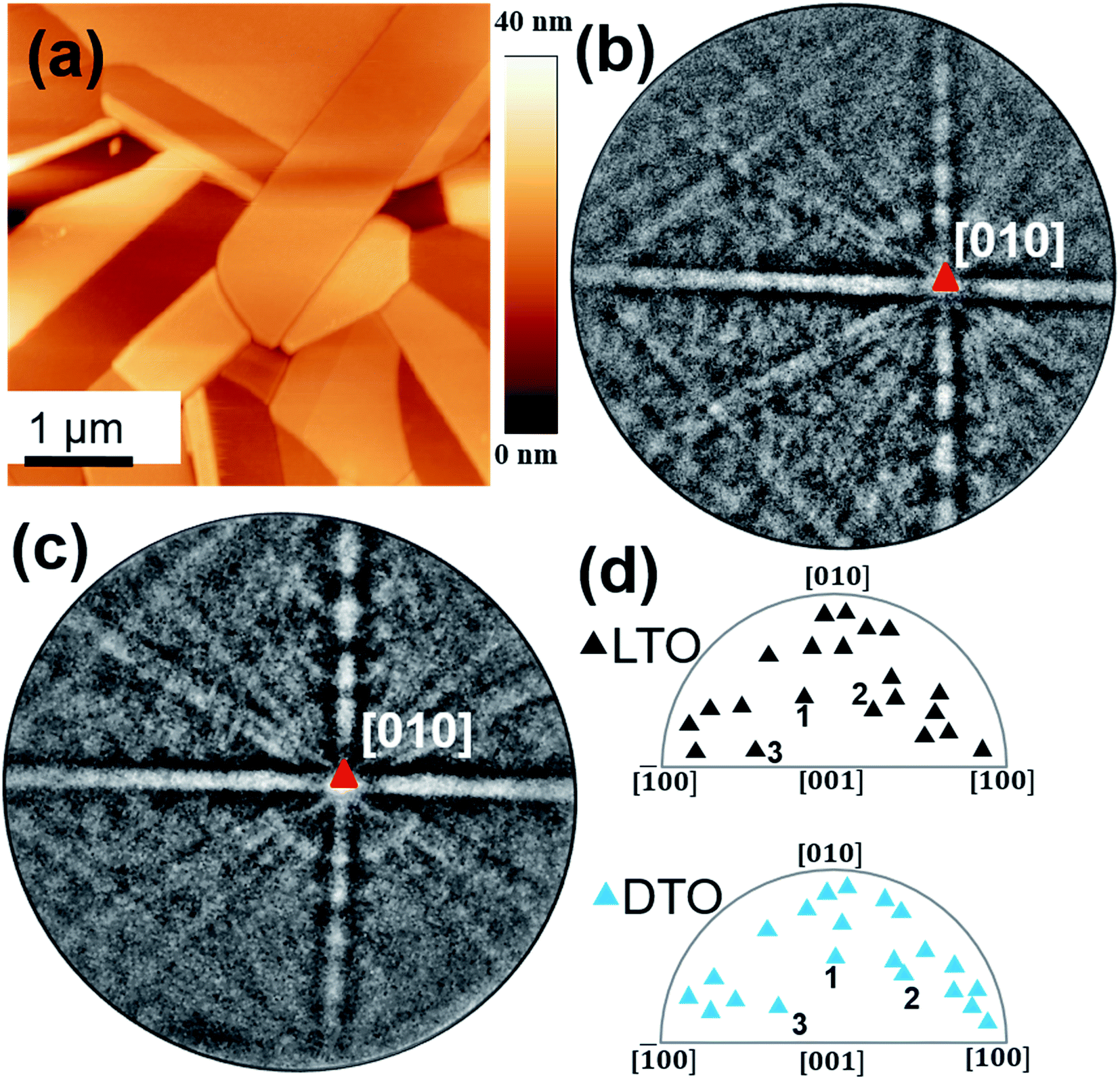 | ||
| Fig. 2 (a) AFM topography image obtained over DTO film of thickness 30 nm grown on thermally etched LTO. EBSD pattern of the (b) bare LTO substrate grain, and (c) from DTO film on the same LTO substrate grain. The red triangle indicates the position of zone axis. The orientation with respect to the surface plane determined from the measured Euler angles in standard angle representation (ψ1, ϕ, ψ2) for LTO grain and DTO film is (202°, 68°, 212°), and (204°, 67°, 212°), respectively. (d) The orientations plot of 21 grain pairs of LTO substrate and DTO film in standard representation of monoclinic inverse pole figure, top and bottom respectively. The black and blue triangle legends represent LTO, and DTO orientations respectively. The three same grain pairs are numbered. | ||
To investigate the crystalline structure of the surface, EBSD patterns were recorded on both the DTO film and the LTO substrate (prior to growth). 21 pairs of grains (film/substrate) were thusly analyzed to understand the epitaxial relationship.4,5,7–10,12 The LTO pattern (Fig. 2b) shows intense, sharp and low symmetry features of the bands, confirming the good crystalline quality, and a monoclinic structure. In Fig. 2b, intense bands are crossed with an angle close to 90° on a zone axis identified as [010]LTO, which confirms the presence of two fold (C2) symmetry axis compatible with a P21 space group. The DTO film grown on this grain exhibits a similar EBSD pattern (Fig. 2c), suggesting the same 110-layered perovskite structure with a similar orientation, and also consistent with a monoclinic structure, which latter was confirmed by SAED. The film pattern is slightly more diffuse, as reported for other films.10 Similar observations were made for all 21 grain pairs discussed herein. As discussed previously,12 automatic indexing of patterns from this complicated low-symmetry structure, is challenging with the commercial software, and improved indexing methods are needed, as discussed elsewhere,9 for generating inverse pole figure maps to illustrate grain over grain growth. However, the patterns collected on individual grains were consistent with the substrate patterns throughout individual grains, indicating reasonable grain over grain growth.12
The epitaxial relationship recorded for 21 pairs of grains is plotted in standard stereographic representations of orientations (see the inverse pole figure in Fig. 2d). All the 21 grain pairs between the LTO substrate and the DTO film exhibit similar orientations, confirming a unit-cell over unit-cell growth (a few examples of grain pairs are labeled 1, 2 and 3 in Fig. 2d). A small misorientation angle is observed, ranging from 3° to 6°, which is mainly attributed to misalignment of the grains resulting from the different positioning of the sample between EBSD runs,5 but may have contributions from film relaxation and growth as well. All these observations are consistent with prior observations of DTO growth on Sr2Nb2O7 substrates,12 which is an orthorhombic 110 layered perovskite. Our observations indicate that high-quality, monoclinic substrates of La2Ti2O7 can be prepared and used to grow epitaxial thin films of metastable Dy2Ti2O7.
3.3 Confirmation of monoclinic DTO lattice
To determine the structure of DTO films, we performed detailed TEM analysis,18–23 which included both electron diffraction (ED) and high resolution TEM (HRTEM). Selected area ED (SAED) patterns were recorded along the [010]LTO (Fig. 3a) and [100]LTO (Fig. 3b) zone axis from a differently oriented film grains period. All ED patterns are a superposition of the ED patterns from the LTO substrate and the DTO film (weaker spots). The ED patterns can be indexed in the P21 monoclinic space group using the following cell parameters a = 7.53 Å, b = 5.5412 Å, c = 13.03 Å (determined by XRD for LTO). There is however clear splitting of diffraction spots along c axis (Fig. 3d inset) due to the different c-parameters for DTO film as compared to the LTO substrate. The sharp reflections and absence of diffuse intensity lines (see the [004] reflection in Fig. 3a along c-axis) are clear indications of the high crystallinity of the film.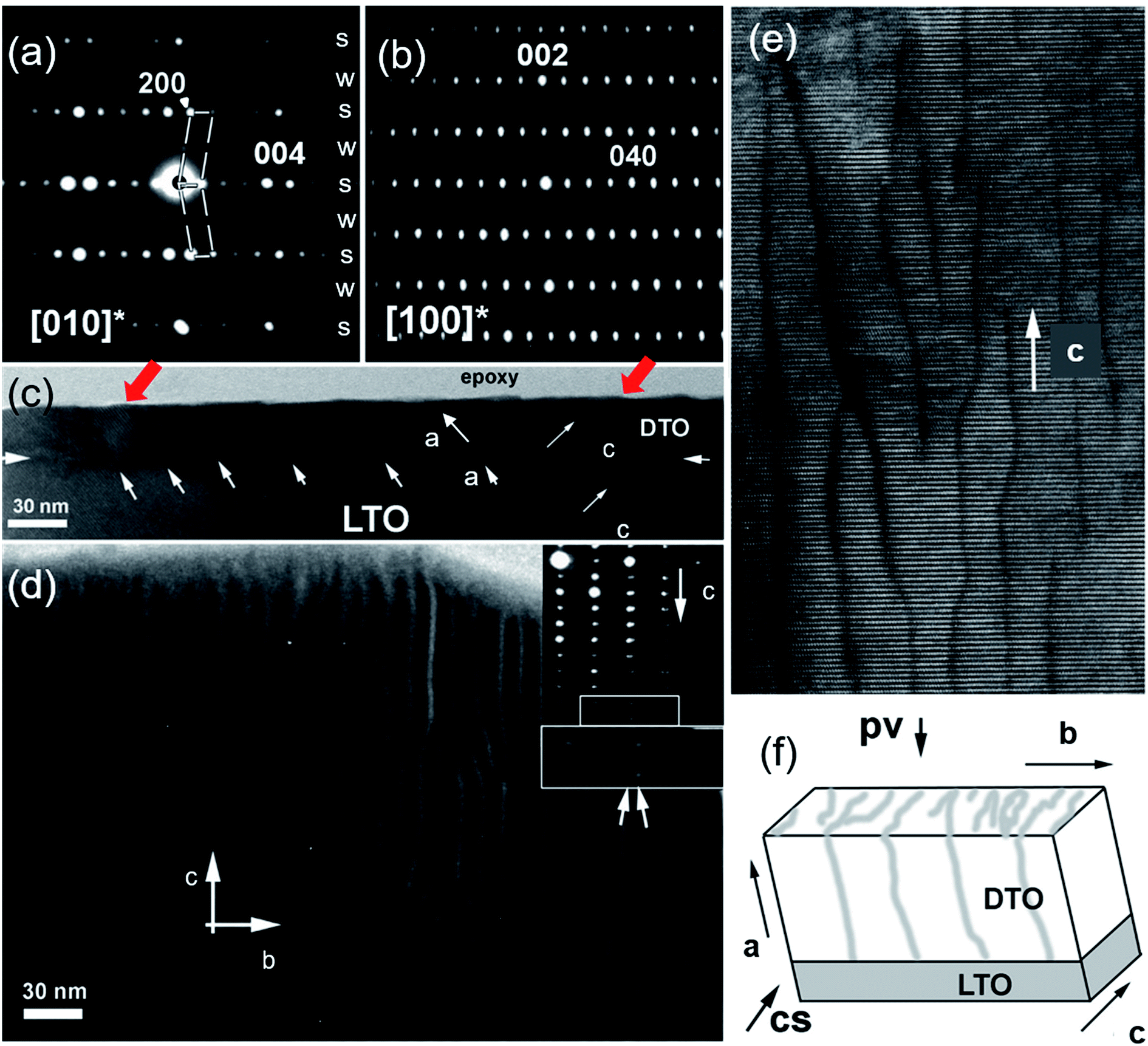 | ||
| Fig. 3 SAED pattern recorded over single grain of DTO film with zone axis (a) [010] and (b) [100]. The highlighted reflections belong to the monoclinic unit cell of space group P21. The rows of strong and weak reflections in [010] ED pattern are representing by s and w, respectively. (c) Cross-section low magnification bright-field TEM image of DTO film grown on LTO substrate showing the epitaxial growth along c-axis. The horizontal white arrow indicates the interface of film/substrate and tilted white arrows for the LAGBs. (d) Plane-view HRTEM image of DTO film grown on thermally etched LTO substrate is shown. The corresponding ED pattern is given as inset. Further, the marked small white rectangle ED pattern is magnified to indicate splitting of spots due to the superposition of the ED pattern of LTO substrate and of the DTO film in big white rectangle. (e) The magnified TEM micrograph of region in (d) is shown to resolve the LAGBs arrangement. (f) The schematic 3D representation of epitaxial growth of DTO film on thermally etched LTO surface is shown. The notation of pv denotes plan view and cs for cross-section view with crystallographic axis indicated. The light grey indicates the LAGBs. | ||
Besides the clear monoclinic angle (β ∼ 98°) in the [010] zone axis which is different from the orthorhombic one for this structure (β = 90°), the [010]DTO ED pattern displays typical characteristics of twinning along the a-axis [100]DTO.18,20 It should be noted that twinning is due to the presence of a mirror plane perpendicular to the c-axis. Strong (s) and weak (w) diffraction rows alternate along the [100] in Fig. 3a and are labelled s and w, which corresponds to diffraction from the cation sublattice and oxygen sublattice, respectively.20 The strong and weak diffraction correspond to miller indices where h = 2n and h = 2n + 1, respectively, with n being the order of reflection.20 The [010] SAED pattern (Fig. 3b) shows sharp diffractions spots and does not show any diffuse streaks along the c-axis. All SAED patterns recorded along [010] and [100] zone axes exhibit sharp diffraction spots, confirming the high degree of structural ordering, confirming the quality of the film confirming latter by HRTEM measurements.
3.4 Mechanism of monoclinic DTO lattice stabilization
A low magnification cross-sectional image (Fig. 3c) and a plan-view HRTEM image (Fig. 3d) were also recorded to understand the DTO film growth. In the cross-section view recorded along [120] zone axis, a sharp contrast at the interface between DTO film and LTO substrate is observed. Further, the DTO film exhibits periodic, inclined boundary-like darker contrast features (depicted with white arrows in Fig. 3c). The plan-view images shown in Fig. 3d and e, taken along the [100] zone axis, clearly illustrates that these boundaries are semi-periodic along the [010]. These boundaries in Fig. 3d are arranged in a Moiré pattern along one direction, and the average mesh size is consistent with boundary separation in the cross-sectional image (Fig. 3c). From an enlarged region (Fig. 3e), these boundaries are not sharp, but curly. It is clear that (001) planes continuously run through the “boundary” and only the contrast (becomes more dark) is changing due to local misorientation from [100] zone axis.These observations suggest that the contrast associated with the boundary is determined by the stress filed around misfit dislocations along LTO/DTO interface. Therefore, the boundaries are low misorientation angle grain boundaries (LAGB). It is well established that small difference between substrate and thin film is accommodated by misfit dislocations. In fact, above a critical thickness, it becomes energetically favorable to accommodate stress by misfit dislocations along film/substrate interface.24
The schematic 3D representation of the boundary planes is given in Fig. 3f. In this figure, the dislocations lines forming LAGBs propagate along the [001] and [100] axes. The boundary abruptly stops propagating along [010]-axis in some regions, while in other regions it bends, and connects with neighbor boundaries. To understand the directional features of the boundary and origin of these boundaries, HRTEM images were recorded in cross-sectional view (Fig. 4a) and plan-view (Fig. 4b). As already mentioned, the [100] and [010] ED patterns are well indexed in a P21 space group. Recorded cross-section HRTEM image and corresponding [120] ED patterns again confirmed the structure of DTO film to be monoclinic. The difference in the unit cell parameters is evident from ED spots (Fig. 4a inset upper right corner) where weak spots belong LTO substrate and strong spots DTO film. The DTO/LTO interface is quite sharp and free of any secondary phase or amorphous layers. Further, the boundary of region (indicated with downward tilted white arrow) does not exhibit stacking faults as viewed from interface to surface of the film in vertical direction. In the HRTEM images, the geometry and position of the white dots, which correspond to projections of the atomic columns on the plane, generally remain undisturbed when crossing the boundary region except for a change in contrast. All these data confirm our suggestion that the contrast change results from the strain field of a LAGB and the presence surrounding strain field. The strain region is imaged as relatively dark contrast because of its slightly different orientation from neighboring grains.
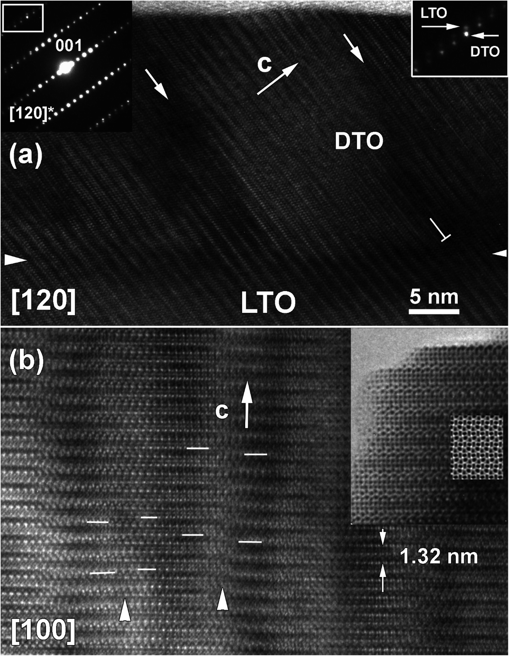 | ||
| Fig. 4 (a) Bright field cross-section [120] HRTEM image of c-axis oriented DTO film over the region in Fig. 3(c) and (e) correspondingly DTO/LTO interface depicted with white arrows heads. The corresponding cross-section SAED pattern is given as inset at left hand corner and indexed based on P21 monoclinic structure (a = 7.816 Å, b = 5.5412 Å, and c = 13.0067 Å with β = 98.698°). The magnified ED pattern is shown in right top corner as inset and indicates the superposition of the ED pattern of LTO substrate (weak spots) and the DTO film resulting in splitting diffraction spots. Noticed presence of misfit dislocation along LTO/DTO interface. (b) Plane-view [100] HRTEM image of selected region in Fig. 3e. The white arrow cap indicates the APBs region. The enlarged HRTEM image of DTO film together with a computer simulated image based on monoclinic structure is given as inset at right hand top corner. | ||
The [100] plan-view HRTEM images gives more information on the film structure (Fig. 4b). The enlarged HRTEM image and overlaid calculated image based on the determined DTO structure shows a good agreement. However, the positions of atomic planes are displaced in some region at 1/3c along [001], direction suggesting of anti-phase boundaries (APBs) at LAGBs. APBs are common defects in layered oxides and have been extensively studied in related layered oxides such as YBa2Cu3O7−δ, Aurivillius and Ruddlesden–Popper phases.25,26 The observed APBs runs over an average thickness of 6 nm. The origin of APBs may be attributed to terraces on the LTO substrate surface, as this has previously been reported for APB.27–29 The terraces can be better seen in Fig. 3c across the LTO/DTO interface. In the films, the APBs propagate up to the surface of the film. The red tilted arrows in Fig. 3c indicate the terrace in the surface of DTO film. A similar view of a terrace is also given in Fig. 4a. Thus, terraces in the substrate surface can lead to stabilization and propagation of these APBs. Further, APB introduce strain owing to local variations in the structural parameters. We propose that the APBs can be related to a misalignment of the extra oxygen layer separating two DyTiO3 perovskite slabs along adjacent TiO6 octahedra. In a perfect crystal there is a perfect periodic stacking of the extra oxygen layer after every four DyTiO3 perovskite blocks along the c-axis19 but at the APB, the extra oxygen layer terminates, intersecting an adjacent perovskite block.
The inset of Fig. 4b shows a bright field HRTEM image of DTO region. According to the simulated image, two dark spots of different sizes, which correspond to Dy (larger dark spot) and Ti (smaller dark spot) can be seen. The interlayer shear boundary is seen as a zig-zag band (Dy–O linkage) between the layers. Again, the simulated image using the monoclinic DTO structure (see its superimposition in the inset) fits well with the experimental data. The presence of internal references from the LTO substrate in the SAED pattern (see the inset of Fig. 3d and 4a) enables one measure of the lattice parameters of the DTO film with a high accuracy a = 7.53 Å, b = 5.31 Å, and c = 13.03 Å and α, β, γ = 90°, 98.65°, 90°. When compared to the LTO substrate, the calculated a and b lattice parameters of DTO film is smaller by 3.6% and 4.1%, respectively due to the chemical difference in cation size of La3+ = 103.2 pm and Dy3+ = 91.2 pm. The monoclinic angle β, and the calculated c lattice parameters are less perturbed. The DTO film lattice accommodates the smaller cation Dy3+ in comparison to La3+ by tilts and/or rotations of the TiO6 octahedra, resulting in slightly different lattice parameters from LTO, and an accommodation via misfit strains with the observed LAGBs/APBs.30,31
In order to shed more light on the strain in the DTO film, Geometric Phase Analysis (GPA) was performed on the Fourier transform (FT) of the filtered HRTEM image (Fig. 5a). The corresponding FT pattern is shown in Fig. 5b; it displays diffuse Bragg intensity, which generally occurs due to the presence of strain and defects in the crystal structure.30 The obtained color-coded GPA strain map (Fig. 5c) of the in-plane [001] lattice parameter shows uniform color when moved from LTO substrate to the film, which confirms the epitaxial growth of DTO with a small strain state and identical lattice d-spacing. The small color variation at the interface of LTO/DTO is due to strain at the interface. The APBs in this region are indicated with vertical white arrows, and the region between APBs appears in bright in color. This indicates that APBs are highly strained in the (ac) plane because they have shorter distances between the adjusted atomic columns. In the GPA strain map, recorded in the out-of-plane direction (Fig. 5d), the film and substrate have large lattice difference resulting in splitting of diffraction spots compared to the in-plane lattice parameter, which are almost equal (see Fig. 5b the corresponding FT pattern). This GPA analysis gives clear indication that DTO film is under compressive strain. The APBs appear yellow, which indicates less strain in comparison to the strain of in-plane lattice parameter in the boundary plane. This indicates that the APBs are strained along the c-axis, and relaxed along a and b axis. Conversely, the crystal region adjacent to LAGBs are relaxed along the c-axis, and strained along the a and b axes.
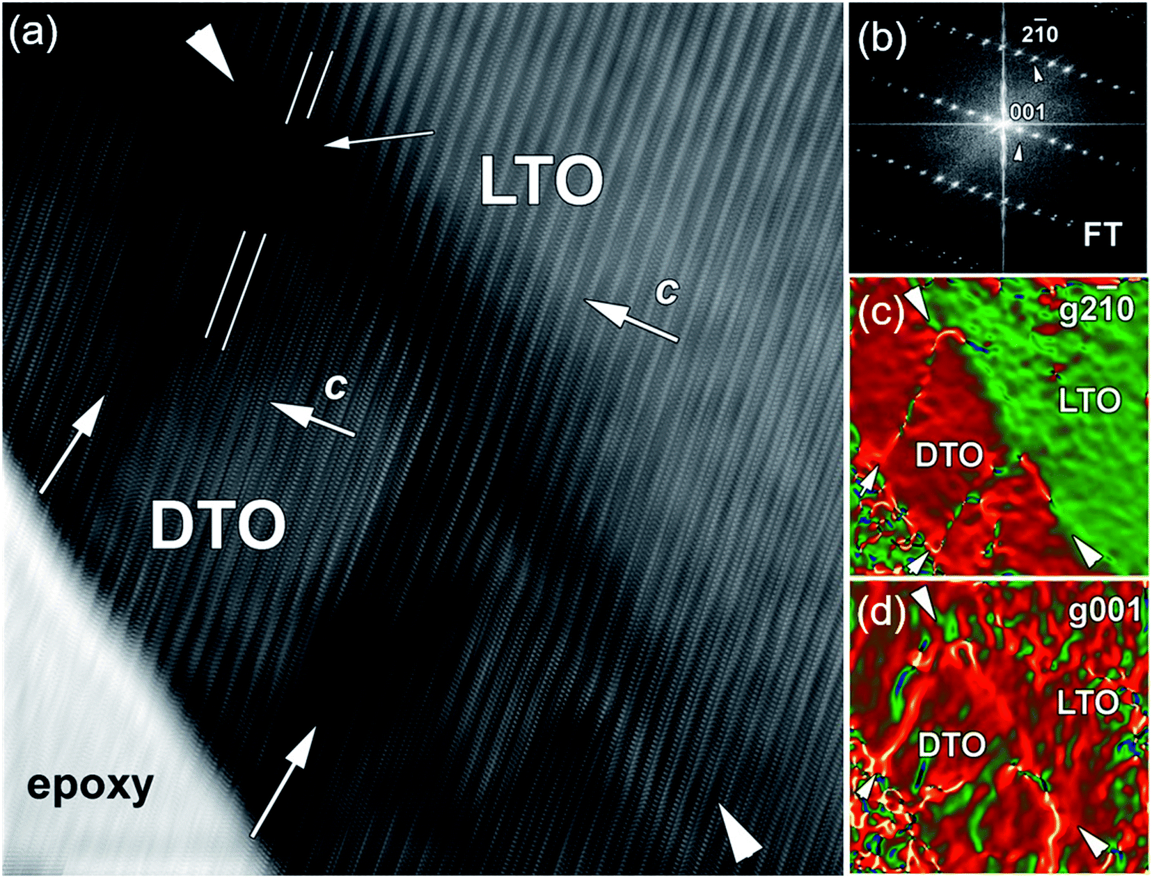 | ||
Fig. 5 (a) Fourier transform (FT) of the filtered HRTEM image (Fig. 4a) and corresponding (b) FT pattern. The colour coded GPA map shows the strain variation along (c) in-plane [001] and (d) out-of-plane [2![[1 with combining macron]](https://www.rsc.org/images/entities/char_0031_0304.gif) 0] directions with reference to LTO substrate. In out-of-plane GPA map the yellow contrast boundaries are clearly visible. It should be noticed that position of this boundaries corresponds to dark region contrasts in corresponding HRTEM image (marked with white arrows). DTO/LTO interface depict with white arrow heads. 0] directions with reference to LTO substrate. In out-of-plane GPA map the yellow contrast boundaries are clearly visible. It should be noticed that position of this boundaries corresponds to dark region contrasts in corresponding HRTEM image (marked with white arrows). DTO/LTO interface depict with white arrow heads. | ||
3.5 Existence of cubic pyrochlore regions
The existence of the cubic pyrochlore should be interpreted as being close in thermodynamics/kinetics to nucleation of the sable phase. Perhaps defects assist that nucleation, and thus it forms and is surrounded by preferred attachment to existing material. It should be noted that inclusions of the stable cubic pyrochlore DTO phase were observed (Fig. 6a). EBSD patterns obtained on such grains agree with there being two phases near the surface: one monoclinic layered perovskite and the cubic pyrochlore phase. An example is given Fig. 6a, where the patterns displays a C3 fold symmetry axis of the [11] zone axis, and a mirror plane, that matches well with the cubic DTO lattice. This indicates that the competition between metastable cubic DTO narrows as the film grows, on certain grains. We believe that, on such grains, there are large terraces on the substrate and that cumulative nucleation events during growth ultimately lead to formation of the stable phase.31
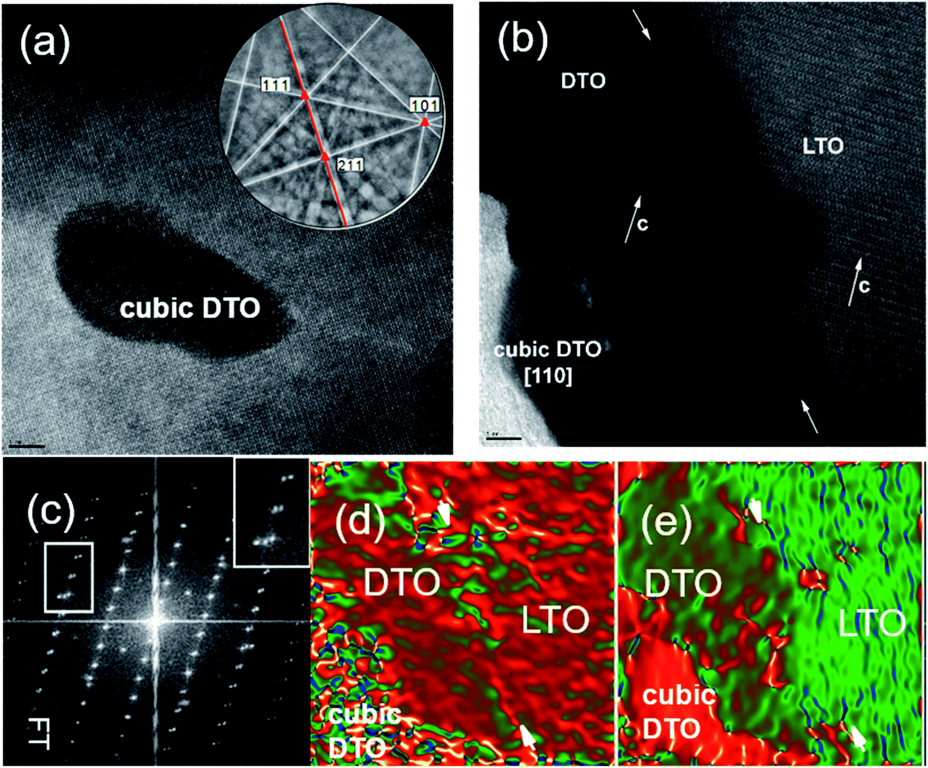 | ||
| Fig. 6 (a) HRTEM plane-view image of DTO film grown on chemically etched LTO substrate. The inset at right hand corner is typical EBSD pattern that well index with cubic pyrochlore DTO lattice is shown. The red triangle indicates the position of zone axis. The red line indicates the mirror plane. The orientation with respect to the surface plane determined from the measured Euler angles in standard angle representation (ψ1, ϕ, ψ2) for CP pattern is (213, 37, 153). (b) HRTEM cross section micrograph of DTO film. (c) FT pattern of the HRTEM image in (a) showing the Bragg's diffraction spots. The inset at right hand corner is the zoomed region of white rectangle at left that shows three spots, which corresponds to LTO substrate, DTO monoclinic and cubic structures within the film, respectively. The colour coded GPA map shows the strain variation of (d) in-plane εxx and (e) out-of-plane εyy with reference to LTO substrate. | ||
Depending on the orientation and substrate surface state, after some thickness, the cubic DTO forms (Fig. 6b). In Fig. 6b, both surfaces of the substrate and the film appear wavy which is attributed to the roughness of the substrate, due to the polishing and chemical etching process used. It should be noted that the film may grow epitaxially with the monoclinic DTO structure along the c-axis, but small areas of cubic structure may grow incoherently at the surface. The color coded GPA strain map (Fig. 6d) taken along the in-plane shows uniformity of colors when moved from LTO substrate to the film, which confirms epitaxial growth and the presence of epitaxial strain in the film. A sharp variation at the interface (dark red) could be observed likely arising from the roughness of the substrate–film interface. The strain variation in the region of marked cubic DTO phase is seen. In the out-of-plane GPA strain map of lattice parameter (Fig. 6e), the film exhibits uniform color that indicates uniform undeformed d-spacing over this region. In this image, the film is more strained compared to the in-plane lattice image, confirming that the film relaxes along the c-axis. Moreover, there are not APBs unlike DTO film grown on smoother LTO substrates as shown in Fig. 3c.
4. Conclusion
In summary, we demonstrate that Dy2Ti2O7 can be stabilized in the monoclinic metastable structure on La2Ti2O7 using the combinatorial substrate epitaxy approach. Using structural characterization including electron backscatter diffraction and high-resolution transmission electron microscopy, the quality of the La2Ti2O7 surface, was highlighted, as was direct epitaxial growth of the metastable monoclinic Dy2Ti2O7 from such substrates surfaces. Detailed structural analysis indicated a variety of defects could be observed, including dislocations, LAGBs, APBs, and regions of secondary phases. The presence of these defects vary from grain to grain, as does the substrate orientation and surface state, and the strain within the metastable monoclinic Dy2Ti2O7 film. In addition, this compound could be ferroelectric similarly to La2Ti2O7 composition, and this is under investigation. Thus, combinatorial substrate epitaxy is promising for the stabilization of the metastable phases having strain and defect engineered states. It represents a promising approach to develop novel/metastable phases of strongly correlated system with properties different from the bulk form, and also to explore the effect of orientation in a systematic manner.Conflicts of interest
There are no conflicts to declare.Acknowledgements
We thank L. Gouleuf and J. Lecourt for technical support. D. P. thanks the Eramsus Mundus Project IDS-FunMat. Partial support of the French Agence Nationale de la Recherche (ANR), through POLYNASH project (ANR-17-CE08-0012), the program Investissements d'Avenir (ANR-10-LABX-09-01) LabEx EMC3, and the program EQUIPEX GENESIS (ANR-11-EQPX-0020) is also acknowledged.References
- D. G. Schlom, L.-Q. Chen, X. Pan, A. Schmehl and M. A. Zurbuchen, J. Am. Ceram. Soc., 2008, 91, 2429–2454 CrossRef CAS.
- J. M. Phillips, J. Appl. Phys., 1996, 79, 1829–1848 CrossRef CAS.
- D. E. Hooks, T. Fritz and M. D. Ward, Adv. Mater., 2001, 13, 227–241 CrossRef CAS.
- N. V. Burbure, P. A. Salvador and G. S. Rohrer, J. Am. Ceram. Soc., 2010, 93, 2530–2533 CrossRef CAS.
- Y. Zhang, A. M. Schultz, L. Li, H. Chien, P. A. Salvador and G. S. Rohrer, Acta Mater., 2012, 60, 6486–6493 CrossRef CAS.
- D. Pravarthana, O. I. Lebedev, S. Hebert, D. Chateigner, P. A. Salvador and W. Prellier, Appl. Phys. Lett., 2013, 103, 143123 CrossRef.
- M. Lacotte, A. David, D. Pravarthana, C. Grygiel, G. S. Rohrer, P. A. Salvador, M. Velazquez, R. de Kloe and W. Prellier, J. Appl. Phys., 2014, 116, 245303 CrossRef.
- M. Santosh, M. Lacotte, A. David, P. Boullay, C. Grygiel, D. Pravarthana, G. S. Rohrer, P. A. Salvador, P. Padhan, U. Lüders, J. Wang and W. Prellier, J. Phys. D: Appl. Phys., 2017, 50, 235301 CrossRef.
- J. Wittkamper, Z. Xu, B. Kombaiah, F. Ram, M. De Graef, J. R. Kitchin, G. S. Rohrer and P. A. Salvador, Cryst. Growth Des., 2017, 17, 3929–3939 CrossRef CAS.
- P. Dhanapal, S. Guo, B. Wang, H. Yang, S. Agarwal, Q. Zhan and R.-W. Li, Appl. Phys. Lett., 2017, 111, 162401 CrossRef.
- D. Pravarthana, M. Trassin, J. Haw Chu, M. Lacotte, A. David, R. Ramesh, P. A. Salvador and W. Prellier, Appl. Phys. Lett., 2014, 104, 082914 CrossRef.
- S. Havelia, S. Wang, K. R. Balasubramaniam, A. M. Schultz, G. S. Rohrer and P. A. Salvador, CrystEngComm, 2013, 15, 5434 RSC.
- M. Gasperin, Acta Crystallogr., Sect. B: Struct. Crystallogr. Cryst. Chem., 1975, 31, 2129–2130 CrossRef.
- M. A. Subramanian, G. Aravamudan and G. V. Subba Rao, Prog. Solid State Chem., 1983, 15, 55–143 CrossRef CAS.
- S. Saitzek, Z. Shao, A. Bayart, A. Ferri, M. Huvé, P. Roussel and R. Desfeux, J. Mater. Chem. C, 2014, 2, 4037 RSC.
- Z. P. Gao, H. X. Yan, H. P. Ning, R. Wilson, X. Y. Wei, B. Shi, H. Ye and M. J. Reece, J. Eur. Ceram. Soc., 2013, 33, 1001–1008 CrossRef CAS.
- A. Ceylan, Mater. Res. Bull., 2008, 43, 1623–1629 CrossRef CAS.
- Z. Shao, S. Saitzek, A. Ferri, M. Rguiti, L. Dupont, P. Roussel and R. Desfeux, J. Mater. Chem., 2012, 22, 9806 RSC.
- T. Williams, F. Lichtenberg, D. Widmer, J. G. Bednorz and A. Reller, J. Solid State Chem., 1993, 103, 375–386 CrossRef CAS.
- H. W. Schmalle, T. Williams, A. Reller, A. Linden and J. G. Bednorz, Acta Crystallogr., Sect. B: Struct. Sci., 1993, 49, 235–244 CrossRef.
- S. Havelia, S. Wang, K. R. Balasubramaniam and P. A. Salvador, J. Solid State Chem., 2009, 182, 1603–1610 CrossRef CAS.
- J. W. Seo, J. Fompeyrine, H. Siegwart and J.-P. Locquet, Phys. Rev. B: Condens. Matter Mater. Phys., 2001, 63, 205401 CrossRef.
- F. Lichtenberg, D. Widmer, J. G. Bednorz, T. Williams and A. Reller, Z. Phys. B: Condens. Matter, 1991, 82, 211–216 CrossRef CAS.
- O. I. Lebedev, G. Van Tendeloo, S. Amelinckx, H. L. Ju and K. M. Krishnan, Philos. Mag. A, 2000, 80, 673–691 CAS.
- F. Tafuri, F. M. Granozio, F. Carillo, F. Lombardi, U. S. Di Uccio, K. Verbist, O. Lebedev and G. Van Tendeloo, Phys. C, 1999, 326–327, 63–71 CrossRef CAS.
- M. A. Zurbuchen, W. Tian, X. Q. Pan, D. Fong, S. K. Streiffer, M. E. Hawley, J. Lettieri, Y. Jia, G. Asayama, S. J. Fulk, D. J. Comstock, S. Knapp, A. H. Carim and D. G. Schlom, J. Mater. Res., 2007, 22, 1439–1471 CrossRef CAS.
- J. Narayan, Acta Mater., 2013, 61, 2703–2724 CrossRef CAS.
- S. J. Pennycook, H. Zhou, M. F. Chisholm, A. Y. Borisevich, M. Varela, J. Gazquez, T. J. Pennycook and J. Narayan, Acta Mater., 2013, 61, 2725–2733 CrossRef CAS.
- V. Narayanan, S. Mahajan, K. J. Bachmann, V. Woods and N. Dietz, Acta Mater., 2002, 50, 1275–1287 CrossRef CAS.
- M. J. Hÿch and L. Potez, Philos. Mag. A, 1997, 76, 1119–1138 Search PubMed.
- C. Ma, M. Liu, C. Chen, Y. Lin, Y. Li, J. S. Horwitz, J. Jiang, E. I. Meletis and Q. Zhang, Sci. Rep., 2013, 3, 3092 CrossRef PubMed.
| This journal is © The Royal Society of Chemistry 2019 |