
 Open Access Article
 This Open Access Article is licensed under a Creative Commons Attribution-Non Commercial 3.0 Unported Licence
Recent progress of solution-processed Cu nanowires transparent electrodes and their applications
Su Ding ab and
Yanhong Tian*b
ab and
Yanhong Tian*b
aCollege of Materials and Environmental Engineering, Hangzhou Dianzi University, 310018 Hangzhou, P. R. China
bState Key Laboratory of Advanced Welding and Joining, Harbin Institute of Technology, Harbin, 150001, China. E-mail: tianyh@hit.edu.cn
First published on 28th August 2019
Abstract
Research on next-generation transparent electrode (TE) materials to replace expensive and fragile indium tin oxide (ITO) is crucial for future electronics. Copper nanowires (Cu NWs) are considered as one of the most promising alternatives due to their excellent electrical properties and low-cost processing. This review summarizes the recent progress on the synthesis methods of long Cu NWs, and the fabrication techniques and protection measures for Cu NW TEs. Applications of Cu NW TEs in electronics, such as solar cells, touch screens, and light emitting diodes (LEDs), are discussed.
1 Introduction
Transparent electrodes (TEs) are crucial to a wide range of modern electronic and optoelectronic devices including light emitting diodes (LED),1–5 touch screens,6–9 solar cells4,10–14 and electronic skins.15–19 As an essential component in device stacks, TEs are highly transparent to visual light and highly conductive, which are difficult to achieve at the same time for common materials. The dominant material used in industry for TEs is a tin-doped indium oxide (ITO) film. Although ITO offers a low sheet resistance at high transmittance (a sheet resistance (Rsh) of 10 ohm sq−1 and a transmittance (T) of 80%, or Rsh = 274 ohm sq−1 and T = 96% (ref. 20 and 21)), there are some issues that need to be addressed. ITO is a kind of ceramic and is inevitably brittle, which prevents its application in flexible and wearable electronics.20,22–25 The price of ITO grows because the supply of indium in the earth is limited (0.05 ppm) and ITO accounts for approximately 3/4 of the global indium consumption.26 Additionally, ITO is deposited or sputtered on substrates by expensive and slow vacuum-based techniques, and the deposition process is inefficient in that only 3–30% indium reaches the target.27 Combining the high price of the raw material and the ineffective processing techniques, the total cost of ITO has been continually increasing during the past decades. As the demand for various electronics is currently growing, the search for new alternatives to ITO using low-cost materials and processing methods has been fiercely investigated by universities and leading companies across the globe.Silver nanowire films have appeared as a promising replacement candidate for ITO electrodes due to their intrinsic high conductivity and special network structure with open holes giving a high transparency. In 2008, silver nanowire (Ag NW) meshes were first used to fabricate TEs, showing equivalent or even better properties than those of traditional ITO films.21 Thanks to their excellent performance, Ag NW TEs quickly attracted the attention of researchers. Cui's group28 coated Ag NW films on flexible substrates using the Meyer rod technique that is widely used in industry, and 8 ohm sq−1 and 80% transmittance are achieved, which out-performs most ITO electrodes, as well as carbon nanotube (CNT) and graphene networks. Lee et al.29 synthesized very long Ag NWs for superior transparent Ag NW TEs (Rsh = 69 ohm sq−1, and T = 95%) and applied them to touch panels. Suganuma's lab30 developed a simple room-temperature washing method to obtain Ag NW TEs with a sheet resistance of 15.6 ohm sq−1 and a transmittance of up to 90%. These achievements prove the potential of Ag NW TEs to replace ITO due to their comparable (or even better) conductivity and low-cost solution processing methods. However, Ag NW TEs also exhibit some drawbacks. Ag is also expensive; is easily sulfurized, even under ambient conditions;31,32 and suffers from electromigration issues.33–35
Copper has an electrical conductivity similar to that of Ag and a significantly lower price (100-times cheaper than Ag). Since copper nanowires (Cu NWs) were first employed to make TEs by Wiley's group,36 research papers about Cu-NW-based electrodes have endlessly emerged. Cu NW TEs possess several merits, as given below: (1) Cu is highly conductive (16.78 nΩ m). As a metallic material, the electrical conductivity of Cu is larger than that of other alternative materials for ITO, including organic conducting polymers (e.g., PEDOT:PSS),37,38 carbon nanotubes,39,40 graphene,8,41–43 etc. (2) Cu is very inexpensive (only 5.8 dollars per kilogram) in comparison with the prices of Ag and raw indium (518 and 210 dollars per kilogram, respectively). The low price of the raw material contributes to the total low cost of Cu NW TEs. (3) Cu NWs are compatible with the full solution processing. Cu NWs have been successfully synthesized by scalable solution methods according to previous papers,36,44,45 and the obtained Cu ink can be printed on various substrates by multiple deposition techniques, e.g., vacuum filtration,46–48 spray coating,49 drop casting,50 Meyer rod coating51–53 and roll-to-roll printing.23 The solution-based fabrications of Cu NW TEs are low cost compared with the vacuum-based physical methods, practical for large-scale production, and amenable to make patterns by overlaying a mask.7,29 (4) Cu NWs are always with a high aspect ratio, which will lead to an improved connectivity and conductivity.54,55 The typically high aspect ratios of Cu NWs yield films with a sheet resistance less than that of films composed of short ones with same material density and a superior mechanical flexibility. Despite these advantages, the oxidation of Cu NWs is severe due to the huge surface area, which will greatly reduce the electrical properties.44,56 The inherent oxidation issue of Cu NWs stands as the core problem of techniques for Cu NW TEs, before their actual application. Here, various techniques to solve the oxidation problem during the fabrication process as well as during the storage period are provided. Although some reviews on metal nanowire TEs have been published,4,27,57–59 a review specific to solution-processed Cu NW TEs with their protection has not been reported, to the best of our knowledge.
In this article, we present a comprehensive overview of the current progress in solution-processed Cu NW TEs including the synthetic approaches to generate Cu NWs, solution processing techniques to improve their conductivity, and protection methods to extend the durability of Cu NW TEs. Finally, we review the applications of Cu NW TEs in touch screens, solar cells and heaters.
2 Solution-phase synthesis of Cu NWs
Cu is characterized as an isotropic face-centred cubic (FCC) structure, and symmetry breaking is an essential key to induce the one-dimensional (1D) growth of Cu NWs. To date, an abundance of approaches have been developed to achieve 1D Cu NWs, such as the electrodeposition method;60 electrochemical nanowire assembly;61 the electrospinning method;62 and template-directed synthesis with anodic aluminium oxide (AAO),63–68 polycarbonate (PC) filters69,70 and DNA71 templates as well as the solution-phase method,44,45,47,72 etc. Among these methods, the solution-phase method has significant advantages due to its facile functionalization, scalability and low cost. The solution-phase method involves the conversion of Cu ions to Cu atoms in the presence of a capping agent, which directs the Cu atoms into a 1D nanostructure. Normally, the morphology of a crystal is determined by the surface energies of different facets, and the final product is always enclosed by low-energy facets.73 Correspondingly, the facets with higher energies disappear due to their rapid growth speed. The presence of a capping agent affects the growth process by selectively binding to specific facets and hindering their growth, leaving behind the final product bound by the specific facets, instead of low-energy facets.74,75 To fabricate Cu NWs, organic amines are usually employed as the capping agent to synthesize Cu NWs by the hydrothermal method,44,45,72,76–78 the hydrazine method,36,52,79–84 and catalytic synthesis,85,86 which will be discussed in the following section.2.1 Hydrothermal method
The surfactant-assisted hydrothermal synthesis of Cu NWs represents one of the earliest synthesis methods employing long-chain carbon amines as a surfactant, such as tetradecylamine (TDA),87 oleylamine (OLA),76,88 hexadecylamine (HDA),44,89 and octadecylamine (ODA).72,77 These surfactants work as a soft template to control the growth direction, whereby the specific crystallographic facets would be limited by the strong combination of surfactants, while other free planes with low energies grow quickly and disappear in the final product. Organic capping agents play a critical role in controlling the morphology of the product.Shi et al.72 synthesized ultra-long and uniform Cu NWs by the reduction of Cu(II) to metallic Cu using ODA as both a soft reducing agent and an adsorption agent. The obtained Cu NWs were reported to have a diameter of 30–100 nm with a huge aspect ratio of up to 105. The authors found that copper(II) chloride (CuCl2) and ODA formed a complex emulsion during vigorous stirring, which was supposed to be a result of the coordination between Cu2+ and ODA molecules. At elevated temperatures, the ODA served as microreactors to generate Cu atoms and were responsible for the formation of the 1D structure. However, in this hydrothermal process, the required synthesis temperature was higher than 160 °C, and the reaction time was as long as 48 hours. Mohl et al.44 described an effective protocol to prepare Cu NWs at a low temperature (120 °C) and within a short reaction time (6–24 hours) by adding a reducing agent of glucose. In the process, glucose acted as a reducing agent producing nanoseeds, which grow into Cu NWs. Additionally, HDA functioned as a template molecule responsible for the preferential growth of Cu atoms. Moon's group77 achieved Cu NWs utilizing various amines, including HDA, ODA, and OLA, and explored the role of alkyl amines. The amine surfactant not only sited specific binding to the crystal plane contributing to the 1D growth for Cu NWs but also underwent complexation with Cu2+ ions to form ligand–metal emulsions promoting the generation of five-twinned Cu seeds. Alkyl amines stabilized the {100} facets of the Cu seeds and hindered their lateral growth, acting as an external confinement for the 1D formation of Cu NWs, as shown in the schematic in Fig. 1. The Cu NWs were always a five-twined structure with {111} facets as twin planes parallel to the long axis of Cu NWs. The Cu atoms were manipulated to form multiple twinned seeds at the nucleation stage with the {111} facets as the external surface. Then, the 1D structure was assembled on the basis of the selective adsorption of HDA onto the {100} facets at the growth stage. Normally, the Cu NWs were bound by ten {111} facets at two ends and five {100} side facets. Jia et al.87 synthesized Cu NWs approximately 40 nm in diameter and a few hundred of micrometres in length by a TDA-assisted hydrothermal method. These ultra-long Cu NWs were successfully achieved using various long-chain alkyl amines. In addition, the authors demonstrated that the Cu NWs could be prepared when the glucose was replaced by other reductants, e.g., vitamin C. However, only cupric chloride (CuCl2) was a suitable Cu source for the Cu NWs—the product consisted of nano- or microparticles using cupric nitrite (Cu(NO3)2) and cupric acetate, while triangular nanoflakes were produced using cupric bromide (CuBr2).
 | ||
| Fig. 1 Schematic of hydrothermal synthesis of 1D Cu NWs.90 | ||
Xia's group45 developed a hydrothermal-like technique to synthesize Cu NWs in sealed vials and in the presence of HDA. After 6 hours of reaction at 100 °C, Cu NWs, with an average diameter of 24 nm and a length from several tens to hundreds of micrometres, were achieved. Additionally, a commercial electric pressure cooker was demonstrated to be successful for the large-scale production of Cu NWs in a similar environment as that of the hydrothermal method.76 A typical reaction was conducted in a 5 L electric pressure cooker at approximately 116 °C, and 2.1 g Cu NWs could be prepared at a cost of only $4.20 per g. Yang's group91 developed a new approach using tris(trimethylsilyl)silane as a mild reducing reagent and OLA as a capping ligand to synthesize ultra-thin Cu NWs (the average diameter was 17.5 nm) without a pressurized environment.
The hydrothermal method for Cu NWs employing long-chain alkyl amines as a surfactant is green, effective, and capable of scalable quantities, providing a competitiveness for Cu NWs in potential applications including low-cost displays, solar cells, and LEDs.92 The obtained Cu NWs possess a huge aspect ratio, showing superiority in high-performance TEs.
2.2 Hydrazine method
Hydrazine has been demonstrated to be a commendable reducing agent for the rapid, large-scale, low-temperature synthesis of Cu NWs in air. Zeng's group79 first presented a facile and large-scale aqueous synthesis of Cu NWs with a diameter of 90–120 nm and a length of 40–50 μm. In this method, an extremely high concentration of sodium hydroxide (NaOH) was applied to prevent the Cu ions from precipitating. Additionally, ethylenediamine (EDA) was used to restrict the morphology of the product. Thanks to the strong reducibility of hydrazine, the reaction was operated at a mild temperature of 60 °C. This hydrazine method was further developed by Wiley's group to generate 1.2 g Cu NWs (200 times that of Zeng's work) within only 1 hour at 80 °C (Fig. 2(a)). The as-prepared Cu NWs presented a spherical Cu particle at one end, from where the Cu NWs sprouted from, as shown in Fig. 2(b). The researchers also concluded that EDA worked as a director for the anisotropic growth of Cu NWs, binding selectively to side facets. The generated Cu atoms deposited on the end of the Cu NWs to elongate the nanowires, as indicated by the growth model in Fig. 2(c).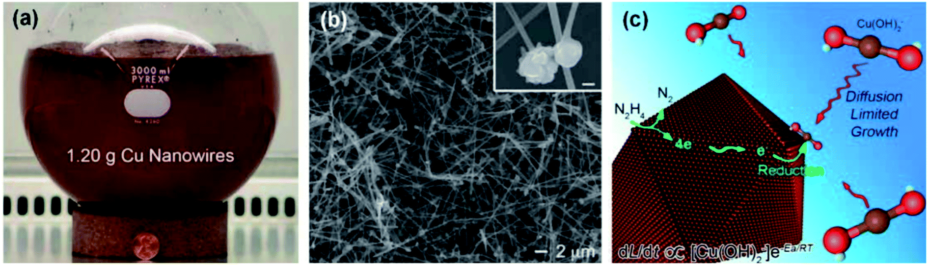 | ||
| Fig. 2 Synthesis of Cu NWs using EDA as a surfactant.36 (a) A photograph of a Cu NW solution. (b) An scanning electron microscopy (SEM) image of Cu NWs. (c) The growth model of the Cu NWs.81 | ||
The growth mechanism for Cu NWs by the hydrazine method was investigated in detail.93 It was concluded that the 1D growth of Cu NWs in solution was driven by axial screw dislocations. The concentration of OH- and EDA could be adjusted to favour dislocation-driven crystal growth, enabling ultra-long Cu NW growth. Wiley's group also researched the growth process of Cu NWs by the hydrazine method.81,82,84,94 The initial mixing of Cu(NO3)2, NaOH, and EDA resulted in a blue complex of Cu(OH)42−, which then turned into Cu(OH)2− and Cu2O seeds while N2H4 was added. These Cu2O nanoparticles were further reduced to Cu aggregates, which served as the seeds that sprouted Cu NWs via the continuous precipitation of Cu atoms. During this process, EDA prevented Cu(OH)2− from completely precipitating in the form of Cu2O nanoparticles and affected the growth rate and aspect ratio of the final Cu NWs. It was also demonstrated that the conversion of Cu(OH)− to Cu NWs could be managed by visible light (not only heat energy) with an energy greater than the band gap of Cu2O. The growth of the Cu NWs could be turned on and off with a light switch, and this phenomenon was used to pattern Cu NWs in specific areas on substrates with a photomask.
The hydrazine method with EDA mediating is performed under atmospheric pressure, at mild temperature, and for a short duration, making this method more practical for large-scale production. The biggest drawback of this method is the toxic hydrazine as one of the most important raw materials for the reaction, and it should be used carefully during practical operation.
2.3 Catalytic synthesis
Catalytic synthesis has been widely used to fabricate a variety of nanomaterials, including metal nanowires and nanorods. Zhang et al.86 reported the nonaqueous synthesis of ultra-long single-crystalline Cu NWs with a diameter of 78 nm in the presence of a piece of Si wafer sputtered with a thin layer of platinum (Pt), also in the reaction medium. The presence of the Pt film catalysed the reduction of Cu2+ ions into metallic Cu atoms, which acted as seeds for the growth of Cu NWs. Without the catalyst, the Cu NWs were not generated, even after 10 hours. Cetyltrimethylammonium bromide (CTAB) and HDA were melted to form a liquid-crystalline medium with a tubular structure. The as-prepared Cu NWs were ultra-long and possessed excellent dispersibility. Nevertheless, this method involved a vacuum sputtering process for the Pt film, which is undesirable for a solution strategy. The researchers further used a solution-synthesized Pt nanoparticle solution to catalyse the growth of Cu NWs. By adjusting the amount of the Pt catalyst, the morphology of the final product could be controlled. Xia's group85 used a palladium (Pd)-mediated growth as a versatile approach to synthesise penta-twinned Cu nanorods with a uniform diameter and controllable aspect ratio. The success of this approach relied on the Pd seeds, which directed the heterogeneous nucleation and growth of Cu along the five-fold axis. Guo and co-workers95 introduced nickel (Ni) ions as the catalyst for preparation of Cu NWs with a high aspect ratio (a diameter of 16.2 nm and a length of up to 40 μm). The authors demonstrated that the active Ni2+ and Cl− ions played a key role in promoting the Cu NWs elongation as well as restricting the lateral diameter.Based on all the above, ultra-long Cu NWs can be successfully achieved through multiple solution processes. The varieties of capping agents and reducing agents show the ability to adjust the dimensions and morphology of Cu NWs. Therefore, it is important to select the proper strategies to make a judicious choice for practical production. The hydrothermal method provides Cu NWs with a greater aspect ratio. Comparatively, the hydrazine method portends a better chance of quantity production and rapid processing. The catalytic method reveals a superior ability to control the dimensions and unitarity of the Cu NWs. The as-synthesized Cu NWs in all these reports could be dispersed in solution by selecting the proper organic solvents or surface-ligand exchange technique, thereby overcoming the aggregation issue,96 to make Cu ink for the coating of Cu NW films.
3 Methods for improving the conductivity of Cu NW TEs
Various coating techniques have been reported to form Cu NW films, including drop casting, vacuum filtration, spin coating, spray coating, and Meyer rod coating.27 After coating, a random network is generated with Cu NWs contacting each other at cross spots, where the resistance is very high due to the loose bonding and the surface coating of organic residuals or other impurities.97,98 An effective way to improve the electrical properties of the network is eliminating the contact resistance between Cu NWs by certain techniques mainly based on two strategies: (1) Increase the contact area between Cu NWs to transfer electrons more efficiently, and (2) remove the impurities on the surface of Cu NWs, including the capping agent used in the synthesis and oxides generated during storage. This section will introduce the existing techniques for enhancing the performance of Cu NW TEs.3.1 High-temperature annealing method
The key issue for the preparation of Cu NW TEs is the rapid oxidation problem accompanying the thermal annealing process in air. Because of the tremendous surface area, the oxidation rate of Cu NWs is substantially faster than that of bulk Cu. After several days storage at room temperature, Cu NWs were coated with a thin layer of cuprous oxide (Cu2O).56 Storing in an organic solvent or adding suitable reductants could partly prevent the oxidation of fresh Cu NWs, however, a slight oxidation of Cu NWs on the surface was inevitable.99 It was found that even freshly prepared Cu NWs were coated with Cu2O at some spots on the surface.49 The instant oxidation problem severely complicates the fabrication process of Cu NW TEs. To improve the conductivity of Cu NW networks, the contact resistance should be decreased through special techniques without the oxidation of Cu NWs.In the year 2010, Wiley's group36 pioneered research on Cu NW TEs and achieved Cu NW TEs with an Rsh of 15 ohm sq−1 and T of 65%. The authors concluded that these Cu NW TEs did not perform as well as Ag NW films due to the bad dispersion of Cu NWs leading to open spaces on the film. Later that year, they dispersed the Cu NWs into a kind of ink formulation and spread it onto a polyethylene (PET) substrate with a Meyer rod to form a thin and uniform film.52 Then, the film was treated at 170 °C for tens of minutes in a hydrogen (H2) atmosphere to remove the surface organics without oxidizing the Cu NWs. After the high-temperature annealing, the flexible Cu NW films were highly conductive and sufficient to power an LED in a circuit, as shown in Fig. 3(a). An SEM image of the Cu NW TEs also indicates the film was coated uniformly (Fig. 3(b)), leading to films with a low resistance at a high transmittance that were equivalent to films of Ag NWs (Fig. 3(c)). On the other hand, as a major advantage, the flexibility of Cu NWs TEs was checked, and the Rsh changed little after 1000 bends. Owing to the excellent performance of the Cu NWs in this paper, the high-temperature sintering method was utilized by many other researchers.76,86,91 Guo et al.95 fabricated Cu NW TEs using a thermal annealing technique at 200 °C in a vacuum oven and achieved a low Rsh of 51.5 ohm sq−1 at 93.1% transparency. The outstanding performance of Cu NW TEs was mainly attributed to the large aspect ratio and firm welding between Cu NWs. After the annealing treatment, the Cu NWs were fused together to form firm thermally welded junctions, becoming conducting.
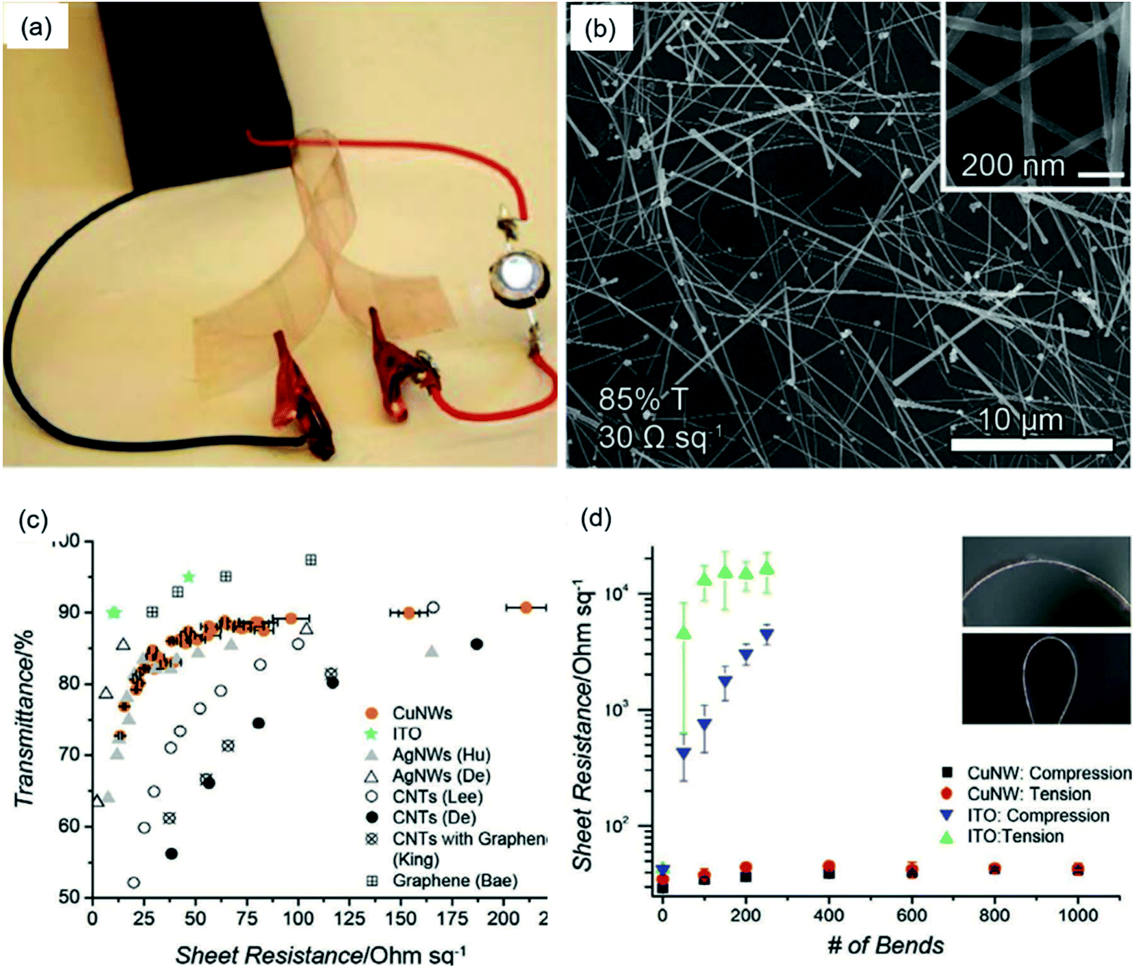 | ||
| Fig. 3 Fabrication of Cu NW TEs and the characterization of their properties.36 (a) A bent Cu NW film completing an electrical circuit with a battery pack and an LED. (b) An SEM image showing a uniformly dispersed network of Cu NWs that was 85% transparent with a Rsh of 30 ohm sq−1. (c) A plot of T versus Rsh for Cu NW TEs. (d) A plot of Rsh versus number of bends for Cu NW TEs. | ||
To clearly study the mechanism of high-temperature annealing method, Sachse et al.100 used a pressing step combined with a sintering process under a hydrogen atmosphere to improve the network performance and achieved highly conductive Cu NW TEs (24 ohm sq−1 at 88% transmittance). The results indicated that although the contacts between Cu NWs were enhanced by the pressing step, the resistance remained high due to the presence of the Cu oxide shell on the surface. The sintering process in a hydrogen atmosphere reduced the surface Cu oxides at elevated temperature, contributing to the high conductivity. Fig. 4 shows the SEM and atomic force microscopy (AFM) images of Cu NW TEs on glass with a transmittance at 87%, after annealed at 200 °C in a vacuum oven for 1 h.95 Clearly, the connecting point between two Cu NWs was fused together after annealing treatment as schematically demonstrated in Fig. 4(b) that the toughing point formed a firm thermo welding junction after annealing. The tight junctions of the Cu NW network were proved to be benefit for the long-term stability of Cu NW TEs. Fig. 4(c) and (d) shows the resistance variation of two groups of Cu NW TEs annealed at 150 °C and 200 °C respectively. The results indicated that TEs maintained unchanged for the samples with transmittance below 60%, on the contrary, the resistance of the samples with higher transmittance increased obviously after 30 days for both two groups. It was because that the influence by the oxidation of Cu would be significant for the sample with incompact NWs. However, the resistance decline of Cu NW TEs was less significant for the group annealed at 200 °C since higher annealing temperature caused a tighter welding junction with less active Cu NW surface, which might lead to a higher oxidation resistance for the Cu NW TEs. The thermo welding of Cu NWs under high temperatures was also studied by Xu et al.101 Highly conductive Cu nanosilk network was achieved after annealed at 200 °C and the firm welding between Cu NW nanosilks was confirmed by AFM. The welding network structure remained stable when the temperature was improved to 400 °C, however, the Cu NWs melted and aggregated into clusters when the annealing temperature beyond 700 °C.
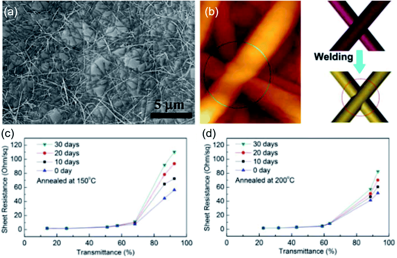 | ||
| Fig. 4 (a) SEM images of the Cu NW TEs on glass substrates with a transmittance at 87%, (b) AFM image of Cu NW after annealing at 200 °C for 1 h, where the welding point has been formed, and schematic of the nanowelding between two NWs before and after annealing. (c) and (d) Transmittance verse Rsh for the Cu NW TEs which were annealed at 150 °C and 200 °C, respectively, and exposed in air for 30 days.95 | ||
It is difficult to reduce the contact resistance between Cu NWs due to their rapid oxidation in air, even at room temperature. Thus, a high-temperature annealing method was always carried out in a hydrogen-based atmosphere or under vacuum. The sintering process decomposed the organic residuals and allowed them to reduce the oxides on the surface of the Cu NWs as well as to weld the Cu NWs together to significantly improve the conductivity of the Cu NW network. However, such an inert atmosphere or vacuum environment is impractical, expensive, and time-consuming, hindering the wide application of the annealing method.
Recently, Yin et al.102 fabricated Cu NW TEs using a so-called solvent dipped annealing method with vacuum-free, transfer-free and low-temperature conditions. After coating the Cu NWs on a glass or PET substrate by the meniscus-dragging deposition method, the films were covered with a small volume of glycerol (GC) or sodium borohydride (NaBH4) solution and heated in the solvent for several minutes. As mentioned above, the natural oxide layer on the surface of Cu NWs increases the contact resistance, even leading to a loss of electrical conductivity. The oxide layer could be eliminated by GC at 140 °C on glass or NaBH4 at 50 °C on PET polymer. Afterwards, these Cu NWs were directly connected with each other and formed a conducting network. Lian et al. proposed a novel annealing and reduction procedure to fabricate Cu NW electrodes with a Rsh of 22 ohm sq−1 and T of 88%. The Cu NWs were first welded by annealing, then polyethylene glycol (PEG) solution was dropped on the surface of the hot film to reduce the oxidation layer. Compared with the high-temperature annealing method in an insert atmosphere, this solvent dipped annealing method presents superiority with its low-temperature, vacuum-free, transfer-free, and simple processes.
3.2 Acid washing method
A simple washing method by glacial acetic acid (GAA) was proved to be effective in purifying Cu NWs and improving the performance of Cu NW TEs.98,103–105 Only by immersing the Cu NW network into a GAA bath for 10 min at room temperature, the performance of Cu NW TEs was dramatically improved to a typical Rsh of 55 ohm sq−1 at a 94% transparency.98 GAA dissolved and destabilized the Cu–amine interaction and dissolved the residual surfactants to achieve ohmic contact between Cu NWs. On the other hand, GAA removed Cu oxides on the surface while not affecting the underlying Cu NWs. This method could be used recurrently to recover the conductivity of Cu NW TEs after being oxidized during storage. Moon's group used lactic acid to fabricate highly conductive and transparent Cu NW TEs with a Rsh of 19.8 ohm sq−1 at 88.7%. Before the lactic acid treatment, the Cu NWs were coated with residual capping agent and surface oxides/hydroxide hindering the transfer of electrons (Fig. 5(a)). The lactic acid treatment effectively removed the chemisorbed capping agent and the surface oxide/hydroxide, allowing tight stacking of Cu NWs, as shown in Fig. 5(b). After the lactic acid treatment, the electrons could be transported between pure Cu NWs (Fig. 5(c)). The acid washing technique is simple, annealing-free, without a protective atmosphere, and could be assembled with roll-to-roll processing in practical production. Despite these advantages, the Cu NWs after acid washing were easily oxidized, and a surface passivation layer was necessary for the long-term stability of Cu NW TEs, such as aluminium-doped zinc oxide (AZO)48 or metal Ni.104 The protection of Cu NW TEs against being oxidized will be introduced in following section.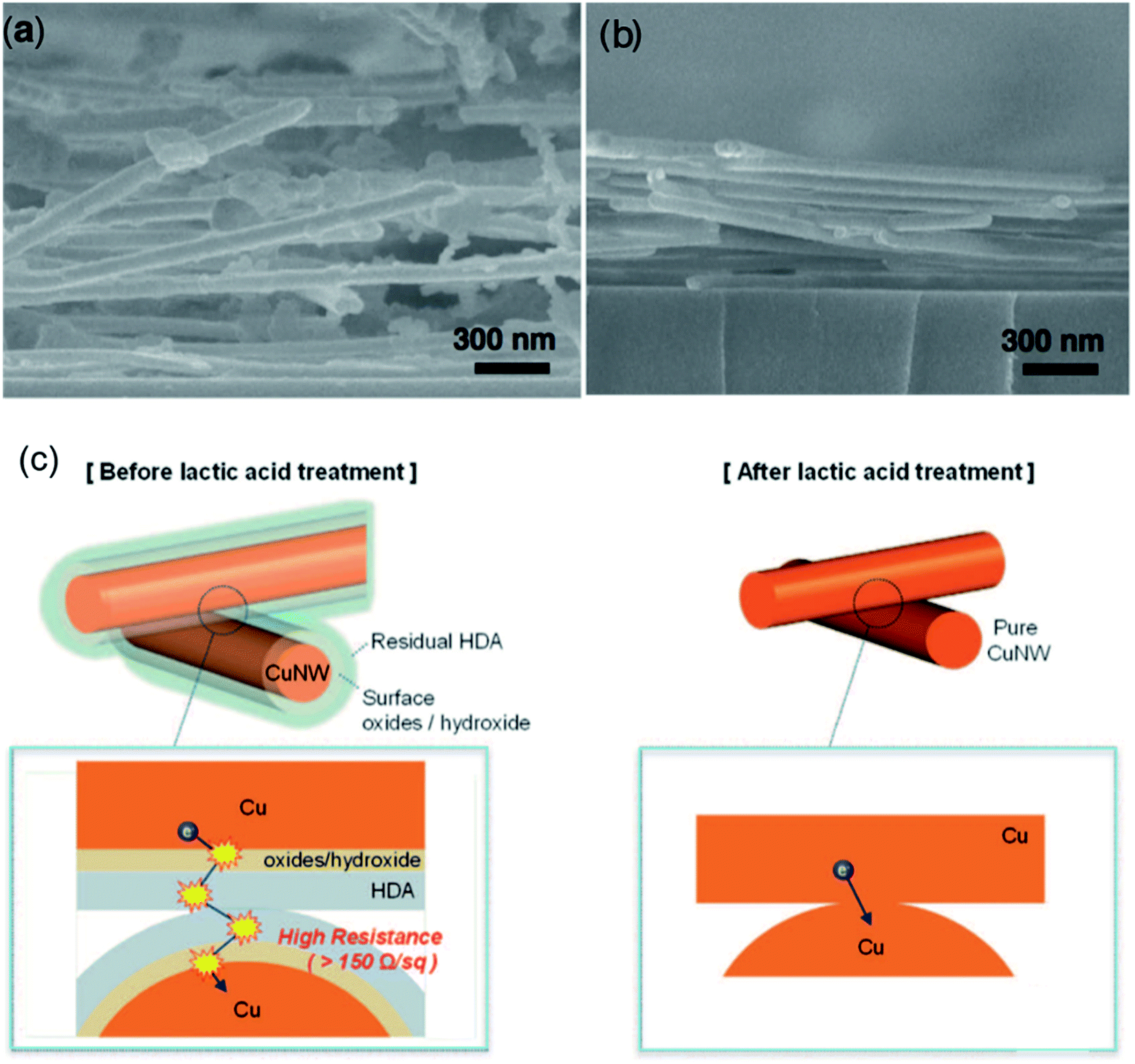 | ||
| Fig. 5 (a) SEM image of Cu NW films. (b) SEM image of lactic acid treated Cu NW TEs. (c) Schematic illustration of the lactic treatment process.48 | ||
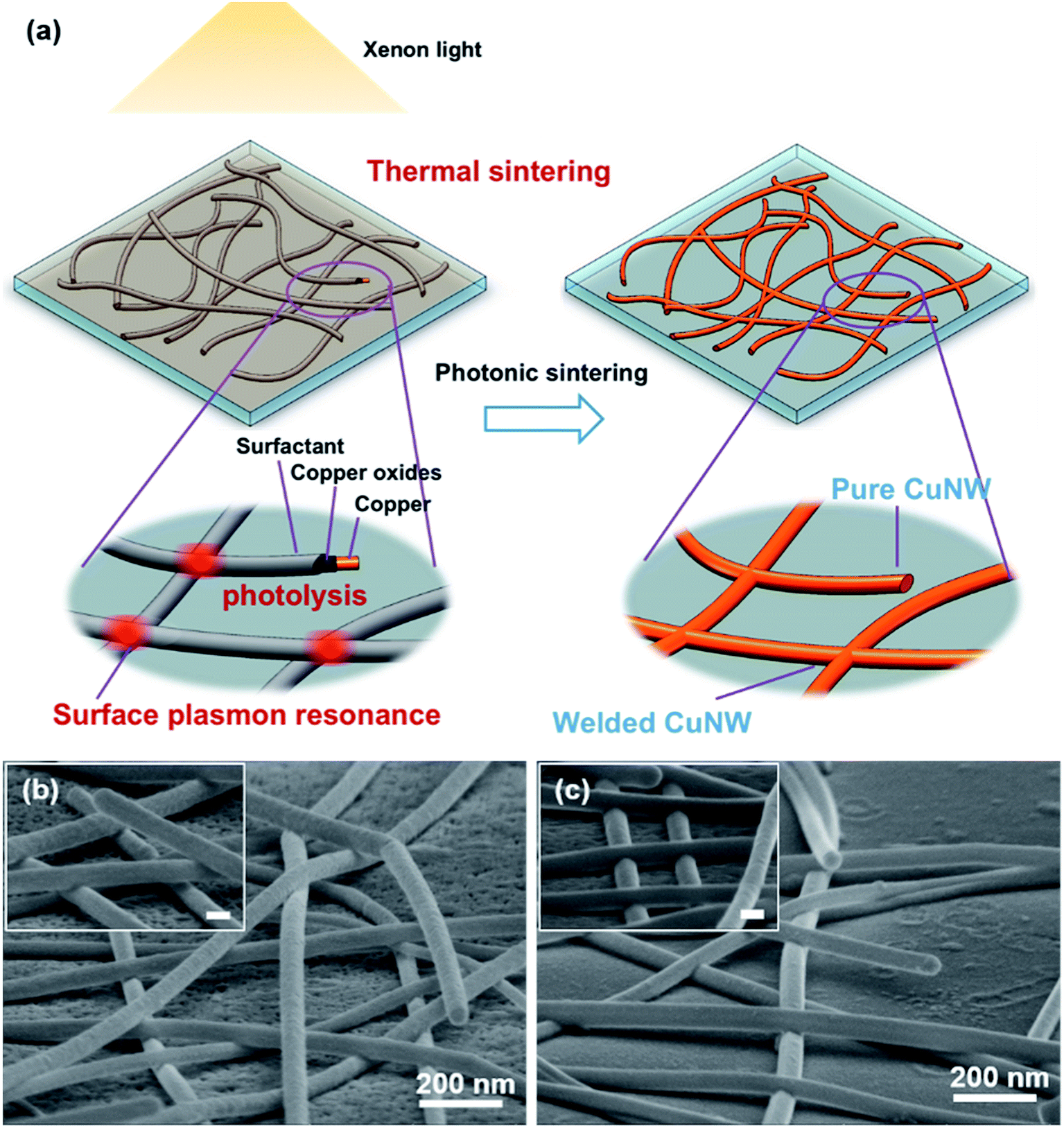
3.3 Photonic sintering method
Ideally, the fabrication process is expected to be operated without the use of high temperatures, a vacuum step, hydrogen protection, or corrosive atmospheres. Photonic sintering method, consisting of xenon light and laser, is considered to be a potential technique to treat metal nanomaterials under mild conditions.49,106 Fig. 6 shows the fabrication process of Cu NW TEs by the laser plasmonic nanowelding technique.106 Compared with traditional bulk heating, the laser nanowelding was located at the junctions between Cu NWs under laser irradiation without destroying other areas of the nanowires (Fig. 6(a)). Through this process, the Rsh decreased significantly since the Cu NWs were welded together to form conductive paths. Thanks to the rapid local laser nanowelding, the oxidation problem was suppressed even in air. In Fig. 6(b), after plasmonic nanowelding in air, the colour change of the Cu NW film was nearly unnoticeable; meanwhile, the colour turned into a dark grey due to severe oxidation with bulk heating. Surprisingly, the oxides could be photothermochemically reduced back to Cu by irradiating a focused laser at the desired area with the assistance of ethylene glycol (EG) as a reducing agent.107 This proposed reduction of Cu oxides to Cu could be repeatedly applied to turn the oxidized Cu NW network into a conductive Cu NW TE, achieving the concept of “nanorecycling” (Fig. 6(c)). The laser plasmonic nanowelding process was carried out at room temperature under ambient conditions without the use of any vacuum/insert gas environment or corrosive atmosphere, resolving the tough oxidation problem for Cu NWs.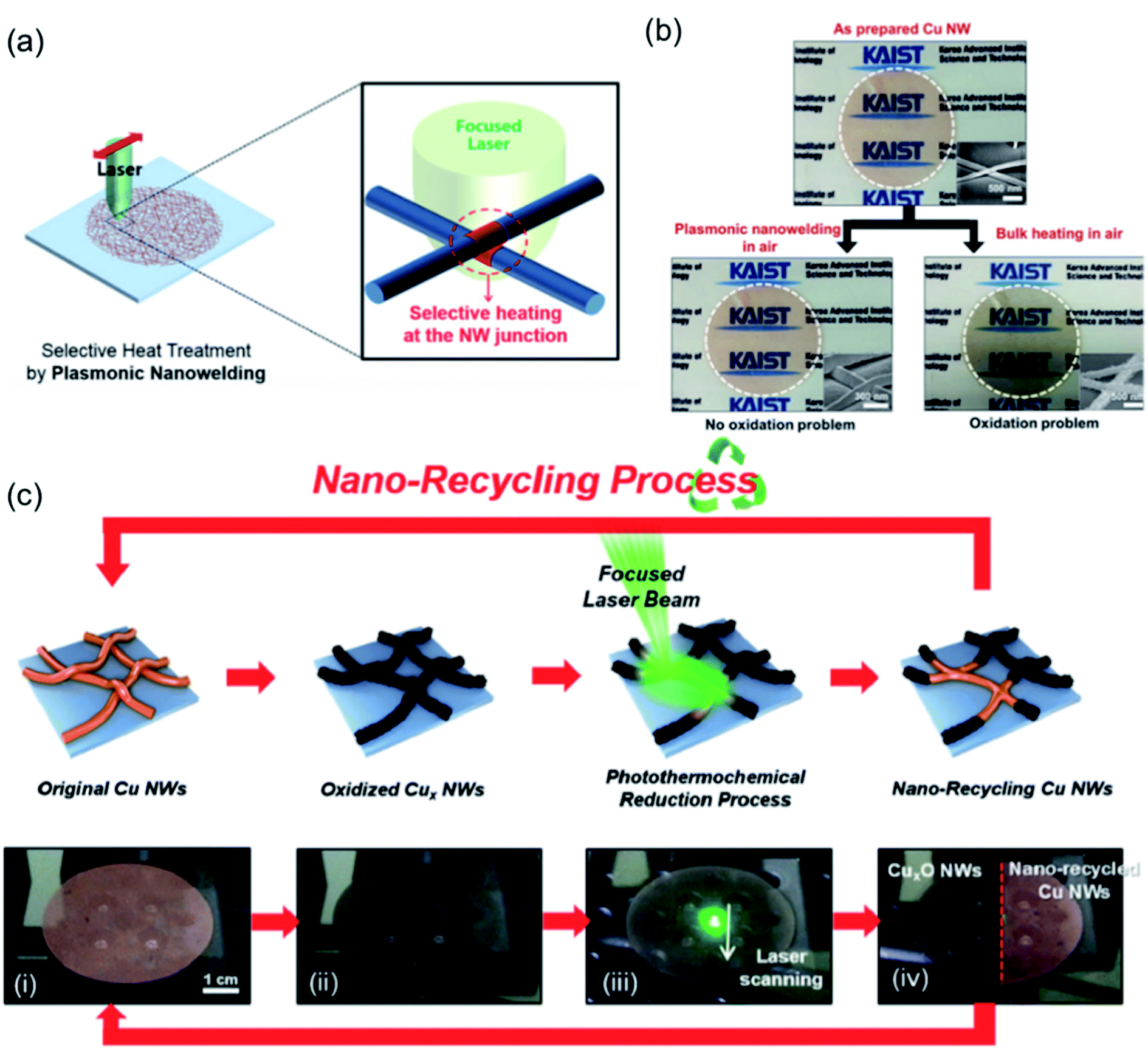 | ||
| Fig. 6 Fabrication of Cu NW TEs by laser plasmonic nanowelding method. (a) Schematic illustrations of the plasmonic laser nanowelding process; (b) optical and SEM images (insets) of as-prepared, laser-nanowelded, and bulk-heated Cu NW films;106 (c) schematic illustration and optical photographs of the “nanorecycling” process.107 | ||
Ding et al.49,108 employed a fast and powerful high-intensity pulsed light (HIPL) technique to fabricate highly conductive Cu NW TEs. The strong light absorption capacity of Cu NWs enabled the welding of nanowires at contact spots due to the conversion of light to thermal energy. The comparison of SEM images of the Cu NW network before and after the HIPL treatment (Fig. 7(b) and (c)) clearly indicated that the distance between Cu NWs was largely changed from a loose overlap to a tight contact. Furthermore, the residual organic surfactant was photolytically decomposed to reduce the surface Cu oxides/hydroxide. As shown in the schematic (Fig. 7(a)), the loosely packed Cu NW network with impurities on the surface was converted into a welded pure Cu NW TE after the HIPL treatment. Mallikarjuna et al.109 developed a photonic welding method using a white flash light (WFL) for preparing flexible Cu NW TEs on PET polymer with a Rsh of 128 ohm sq−1 and 95% transparency within only 5 ms. Due to the localized heating and subsequent welding of the junctions between Cu NWs, the PET polymer was not damaged during the photonic welding process, providing opportunities for the production of flexible optoelectronic devices. Moon's group110,111 also used the intense pulsed light (IPL) irradiation method to remove organic species and to form tight junctions between Cu NWs without any atmospheric control. After IPL irradiation, the Cu NWs were partly embedded into the surface of the polymer substrate without a declination in transmittance. The embedding of Cu NWs in the polymer brought about a series of advantages, including excellent adhesion between the Cu NWs and substrate, good mechanical flexibility and oxidation resistance. The photonic sintering method avoids the use of a complex protective atmosphere, high temperatures, and corrosive solvents, showing a feasibility for the fast and scalable production of high-performance Cu NW TEs.
 | ||
| Fig. 7 (a) Schematic representation of the HIPL treatment of a Cu NW TE; SEM images of a Cu NW network (b) before and (c) after the HIPL treatment.49 | ||
The photonic sintering technique becomes an effective approach for the robust fabrication of Cu NW TEs, thus, more deeply researches about the mechanism are published.112–114 As mentioned above, three types of light interactions have been described in the photonic sintering process as presented in Fig. 8(a). (1) The Cu NWs were locally connected at the intersections by the plasmonic welding. (2) The oxidized Cu NWs were reduced into pure Cu NWs by the photochemical reaction. (3) The Cu NW network is interlocked in the melting surface of the polymer substrates.115 The reactions between the light and the Cu NWs are also simulated by finite difference time domain (FDTD) software to verify the above conclusions. The light is strongly adsorbed by the Cu NWs around 600 nm when the field is directed perpendicularly to the top Cu NWs, indicating that intensive heat could be produced by electromagnetic interactions. The generated heat facilities the welding and interlocking process of Cu NW networks. The heat generation is decreased after the Cu NWs are welded together, showing self-limiting of the photonic sintering process. The microstructure of the Cu NWs at the junctions shows robust contact formation of the Cu NW network without damaging the other parts of the nanowires. The FDTD simulation helps a lot to understand the mechanism of the photonic process and agrees well with the experiment results. The photonic sintering method induced by the plasmonic effects is a novel and promising approach, which is expected to combine with the roll-to-roll process for large scale production in industry.
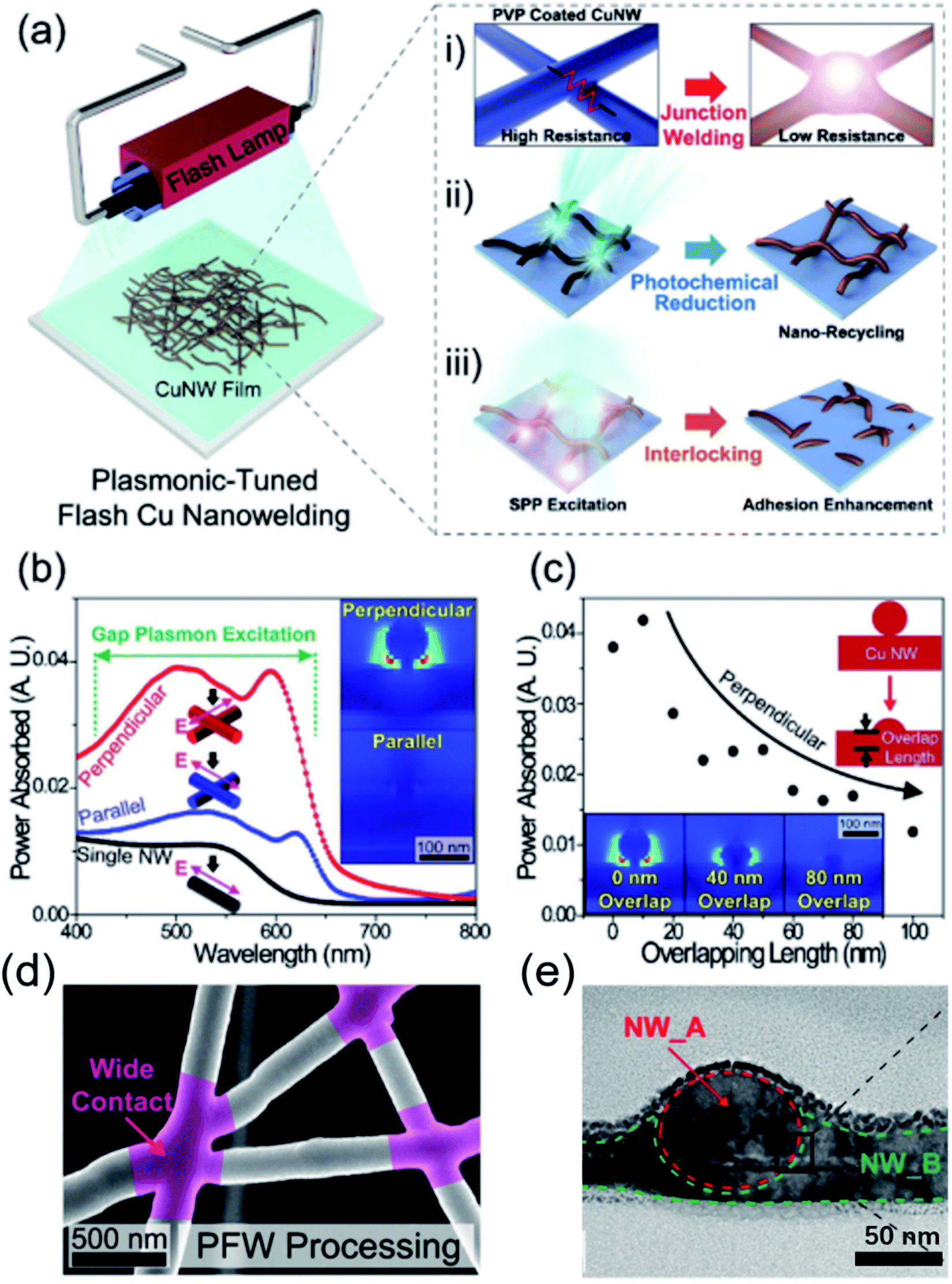 | ||
| Fig. 8 (a) Schematic illustration of the Cu NW plasmonic-tuned flash welding (PFW) process. (b) Spectral and polarization-dependent simulations of local light absorption for the Cu NW junction from 400 to 800 nm wavelength. The inset shows the field enhancement response under the visible light (wavelength of 600 nm) for light polarized perpendicular/parallel to the first NW. (c) Local heat generation as a function of Cu NW overlap length, which shows the self-limiting nature of the PFW process. The insets show field distribution simulations as a function of Cu NW overlap length. (d) A plane-view SEM image of PFW-treated Cu NWs. (e) A plane-view transmission electron microscope (TEM) image of fused Cu NW junction.115 | ||
3.4 Plasma treatment
Wang et al.116 developed a new, simple and large-area scheme for the low-temperature fabrication of Cu NW TEs by the hydrogen plasma technique. The etching and reductive effect of the hydrogen plasma cleaned the surface of the Cu NWs, facilitating the diffusion of Cu atoms between nanowires. In addition, the discharge hydrogen plasma generated a purple light, which greatly enhanced the welding of Cu NWs at the contact spots due to the thermal heating caused by the surface plasmonic resonance effect. After the plasma treatment, Cu NW TEs with an excellent performance of 19 ohm sq−1 at 90% transparency were achieved.In this part, we introduced four types of treatment methods for preparing Cu NW TEs, employing different strategies to deal with the oxidation problems of Cu NWs and to enhance the welding between nanowires generating high-performance TEs. The high-temperature annealing method traditionally improved the contacts between Cu NWs by heating and employing vacuum or a hydrogen-based atmosphere to avoid the oxidation of tiny Cu NWs at elevated temperatures. The acid washing method simply removed the surface impurities by diluted corrosive acids and achieved direct contact between pure Cu NWs. The photonic sintering technique converted the light energy into thermal energy to sinter the Cu NWs to form tight junctions, as well as to remove the surface oxides and organic residuals by photothermochemical reactions. The hydrogen plasma treatment cleaned the surface of Cu NWs including the oxides and organics, and at the same time, welded the Cu NWs at the contact spots by thermal heating. However, before the practical application of Cu NW TEs in devices, the stability of the Cu NW TEs should be checked and ensured, which will be studied in the following part.
4 Protection of Cu NWs from oxidation
As mentioned above, the facile oxidation problem of Cu NWs severely hinders their application on TEs. Although high-performance Cu NW TEs can be achieved by various techniques, the conductivity of as-prepared Cu NW TEs degrades rapidly in several days without protection. Luckily, protection methods for Cu NW TEs have been reported to prolong their long-term stability. Normally, to prevent a Cu NW network from oxidation, the Cu NWs were always coated with a passivation layer, including stable metals or metal oxides,17,117,118 graphene119 and organics.120–1234.1 Metal and metal oxides
Wiley's group coated Cu NWs with a Ni shell to synthesize cupronickel nanowires (CuNi NWs) for preparation of CuNi NW TEs.124 The diameter of the Cu NWs was enlarged from 75 nm to 116 nm due to the coating of the Ni shell, as indicated in Fig. 9(a) and (b). Although the transmittance of the network decreased when more Ni was added, a high-performance CuNi NW TE with a Rsh of 60 ohm sq−1 at 84.3% transparency was obtained (Fig. 9(c)). Thanks to the coating of Ni, the nanowire films were significantly more stable than Cu NW and Ag NW films, as shown in Fig. 9(d). The Rsh of CuNi NW films remained remarkably stable over 30 days, showing good oxidation resistance at elevated temperatures. Afterwards, the authors introduced an electroless plating process by dipping a Cu NW network in a Ni plating solution to make a CuNi NW TE with a high stability comparable to that of Ag NW films.104 Zeng's group also synthesized Cu@Cu4Ni nanowires via a one-pot method and fabricated TEs using the as-prepared Cu@Cu4Ni nanowires with ultra-high stability.125 Wang et al.126 simultaneously obtained two kinds of bimetallic nanowires, Cu@Ni and Cu@Ag nanowires, and employed them to fabricate anti-moisture and anti-thermal TEs. However, the coating of a Ni or Ag shell to protect the Cu NWs came with a sacrifice of film transmittance since the Ag and Ni shells always showed a grey colour. To prevent the decline in transparency, Wiley's group presented a general strategy for protecting Cu NWs against oxidation with Zn, Sn and In as a passivation layer by a solution-phase process.87 By selectively plating these metals only on the surface of Cu NWs, without deposition on the open areas, the transmittance of the films only decreased 4–9%. Furthermore, by exposing the core–shell nanowires to oxidizing conditions, the transmittance could largely recover due to the formation of a transparent shell of metal oxides/hydroxides. Thus, highly conductive and stable Cu–Zn nanowire TEs with a Rsh of 29 ohm sq−1 and T of 84% were achieved.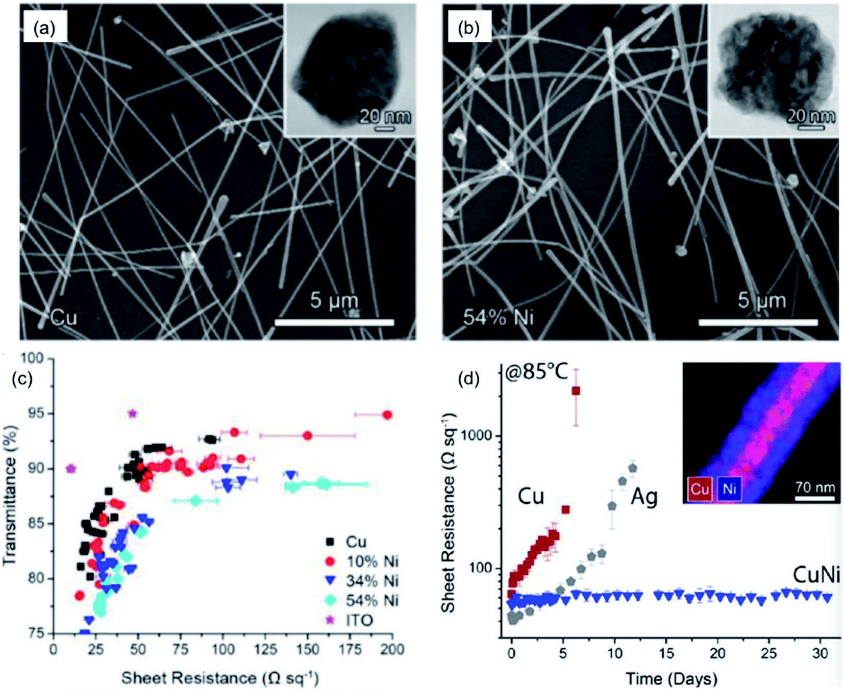 | ||
| Fig. 9 SEM images of Cu NWs (a) before and (b) after the coating of Ni to a concentration of 54%. The insets show the cross-sections of the Cu NW and CuNi NW. (c) Plot of T verse Rsh for films of Cu NWs, CuNi NWs, and ITO on glass. (d) Plot of Rsh verse time for films of Ag NWs, Cu NWs, and CuNi NWs stored at 85 °C.124 | ||
Cui's group127 utilized aluminium-doped zinc oxide (AZO) and aluminium oxide (Al2O3) as passivation layers. The AZO shell was coated on eletrospun Cu nanofibers by the atomic layer deposition (ALD) technique and remarkably enhanced the durability of the Cu NW TEs. After oxidation at 160 °C in dry air or 80 °C in 80% relative humidity, the resistance of the AZO protected Cu nanofibers only increased 10%, whereas bare Cu nanofibers became insulating. Moon's group also modulated the surface of Cu NW networks by fully coating an AZO layer by the magnetron sputtering method.48 The embedded structure of Cu NWs with AZO dramatically improved the oxidation resistance of the Cu NWs, whereby the resistance was nearly unchanged at 80 °C, even after one week.
4.2 Graphene and reduced graphene oxide (RGO)
Two-dimensional graphene and RGO have attracted substantial attention due to their unique properties, including a high thermal conductivity, high electrical conductivity and high anti-corrosion performance. Kholmanov et al.128 prepared RGO/Cu hybrid films by transferring RGO films onto a Cu NW network. The 2 dimensional (2D) RGO platelets yielded hybrid films with an improved electrical conductivity, film continuity, and better adhesion to substrates. Furthermore, the fully coated RGO layer protected the Cu NWs from oxidation under harsh environments, such as high temperatures and acid solutions. Shi et al.129 fabricated graphene covered Cu NW TEs and investigated their long-term oxidation resistance. The graphene covered Cu NW TEs exhibited a strong oxidation resistance, as evidenced by the resistance only increasing 0.27 after 45 days storage. The graphene layer was supposed to prevent the permeation of oxygen and water, decelerating the oxidation of Cu to Cu2O and hindering the transformation of Cu2O to CuO. Therefore, a more perfect coating or multi-layer graphene would show a better performance in protecting the Cu NWs from oxidation.Xu et al.101 directly fabricated a 3D coating layer using graphene on a Cu nanosilk network via the chemical vapor deposition (CVD) method. The graphene shell improved the antioxidizing ability of the original Cu nanosilks, and the resistance was kept stable under ambient conditions for 2 months with the protection of the graphene layer. Ahn et al.130 first synthesized a Cu NW–graphene core–shell structure by the low-temperature plasma-enhanced CVD (LT-PECVD) method at 400 °C, as shown in Fig. 10(a). After the LT-PECVD treatment, the Cu NWs were fully covered with graphene of which the thickness was approximately 5 nm (Fig. 10(b)). The Cu NW–graphene nanostructure was used to fabricate TEs, which showed remarkable thermal oxidation stability due to the tight encapsulation of the Cu NWs by the gas-impermeable graphene shell. As shown in Fig. 10(d), the Rsh of Cu NW TEs quickly increased in 2 days, while the Rsh only raised 9% after 30 days for Cu NW–graphene TEs. To avoid the usage of an expensive CVD process, Dou et al.131 wrapped graphene oxide (GO) sheets on the surface of Cu NWs to form a Cu NW@GO core–shell structure by a simple solution method. The GO shells could be reduced by mild thermal annealing in a forming gas atmosphere, and high-performance Cu@RGO core–shell nanowire TEs were obtained (Rsh were 14.8 ohm sq−1 and 75.0 ohm sq−1 at 86.5% and 93.9% transparency, respectively). Compared with the poor stability of Cu NW TEs, the RGO wrapped Cu NW films showed no obvious degradation in Rsh since the enhanced packing of RGO nanosheets limited the diffusion of oxygen through the protective layer.
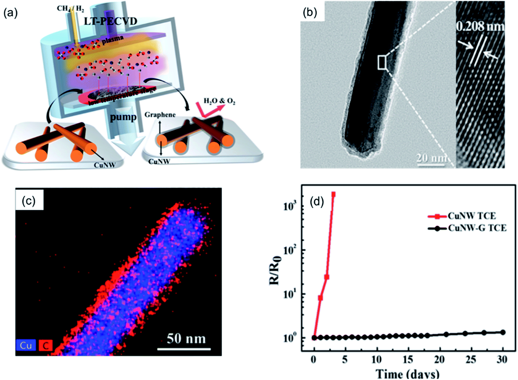 | ||
| Fig. 10 (a) Schematic illustration for the synthesis of the Cu NW–graphene core–shell nanostructure by the LT-PECVD process. (b) TEM image of the Cu NW–graphene core–shell nanostructure. (c) Energy disperse spectroscopy (EDS) mapping analysis of a Cu NW–graphene core–shell nanostructure. (d) Rsh changes for Cu NW and Cu NW–graphene TEs during a stability test in air at room temperature for 30 days.130 | ||
4.3 Organic layer
Chen et al.132 reported a facile solution method to embed Cu NWs into the conducting organic poly(3,4-ethylenedioxythiophene):poly(styrenesulfonate) (PEDOT:PSS) polymer on a PET substrate. The PEDOT:PSS semi-solidified polymer was pre-coated on PET films followed by the deposition of Cu NW ink by the spray method. Then, the sample was annealed and pressed to form a Cu NW-PEDOT:PSS composite TEs. The PEDOT:PSS polymer worked as a binder to enhance the joining between the Cu NWs themselves and between the nanowires and PET. Meanwhile, the PEDOT:PSS protected the Cu NWs from erosion, and the conductivity of the Cu NW-PEDOT:PSS TEs remained stable in air. Chu et al.105 prepared Cu NW TEs by partially embedding the Cu NWs into a poly (methyl methacrylate) (PMMA) matrix on a PET substrate. After the coating of PMMA, the surface roughness of the Cu NW network was largely decreased compared with that of a bare Cu NW network due to the partial embedding of Cu NWs into the PMMA polymer, as shown in the AFM image in Fig. 11. The Cu NW/PMMA composite TEs showed an improved oxidation stability and a resistance increase from 6.1 to 21.3 ohm sq−1 after 30 days under ambient conditions (Fig. 11(c)). The Cu NW/PMMA composite TEs also remained significantly more stable in a sodium sulfide (Na2S) solution compared with the Cu NW and Ag NW TEs (Fig. 11(d)). The embedding of Cu NWs in a polymer structure was also achieved by the one-step IPL technique, as mentioned above.110 The Cu NWs were instantly heated and self-embedded into the plastic polycarbonate (PC) substrate after the IPL treatment, which improved the oxidation stability of Cu NW TEs.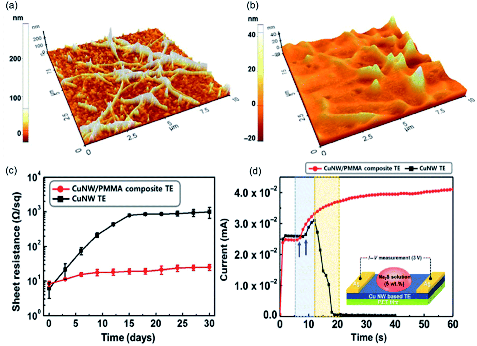 | ||
| Fig. 11 AFM topographic images of (a) Cu NW TEs and (b) Cu NW/polymer composite TEs. (c) Change in Rsh of Cu NW and Cu NW/PMMA composite TEs stored under ambient conditions for 30 days. (d) Changes in the current of Cu NW and Cu NW/polymer composite TEs over time, upon treatment with aqueous Na2S solution.105 | ||
Given the increasing importance of Cu NW TEs, the protection of Cu NWs from oxidation becomes essential. According to the above description, there are some methods to coat passivation layers on Cu NWs or above the Cu NW network, including stable metal/metal oxides, graphene/RGO, and organic layers. The metal coatings are always selectively coated on Cu NWs by a simple solution process; however, the metal layer will decrease the optical performance of Cu NW TEs. Metal oxides show the perfect protection for Cu NWs from oxidation; meanwhile, the fabrication process often refers to expensive sputtering or deposition techniques. The 2D graphene/RGO sheet limits the diffusion of oxygen and water, cutting off the transformation of metal Cu to oxides. The organic layers are more stable; however, the partially embedded structure of Cu NWs cannot perfectly prevent the oxidation of Cu NWs. We believe these protection methods for Cu NW TEs will be further improved before their application in various devices.
5 Applications
A lot Kinds of flexible electronics have emerged, including attachable antenna to receive signals,112 wearable nanogenerators,133,134 adhesive sensors to monitor the movements of human,135 etc.. The essential advantage of flexible electronics is they are bendable, stretchable and deformable while maintaining good conductivity and reliability. Moon's group103 introduced a 3-dimensional-structured electrode based on Cu NWs and helical polydimethylsiloxane (PDMS) matrix to facilitate high stretchability of 700% without degrading the conductivity. Hu et al.136 fabricated conductive, transparent and stretchable composite electrode consisting of a CuNW network embedded in the surface layer of the polyurethane (PU) matrix by a transferring process, which was usually used to make stretchable conductors. The as-prepared Cu NW-PU composite electrodes maintained high conductance (Rsh < 100 ohm sq−1) even at tensile strain up to 60% thanks to the enhanced bonding between CuNWs and PU substrate. Han et al. further compared the stretchable property of Cu NWs electrodes before and after photonic sintering process as shown in Fig. 12. As mentioned above, the Cu NWs could be embedded on the surface of the substrates with strong adhesion after photonic treatment, leading to a better stability under tensile strains compared with untreated Cu NW electrodes. Simultaneously, the mechanical properties of the Cu NW electrodes are tested in terms of bending and folding. The resistance of the laser nanowelded Cu NW conductor showed little change in its resistance even after 20![[thin space (1/6-em)]](https://www.rsc.org/images/entities/char_2009.gif) 000 times bending cycle or 0° folding. Regrading of the excellent performance of Cu NW TEs under various mechanical strains, Cu NW TE is expected to replace commercial ITO for applications in various electronics, such as solar cells, touch screens, LEDs and so on, which has been reported in existing references, as shown in Fig. 13.
000 times bending cycle or 0° folding. Regrading of the excellent performance of Cu NW TEs under various mechanical strains, Cu NW TE is expected to replace commercial ITO for applications in various electronics, such as solar cells, touch screens, LEDs and so on, which has been reported in existing references, as shown in Fig. 13.
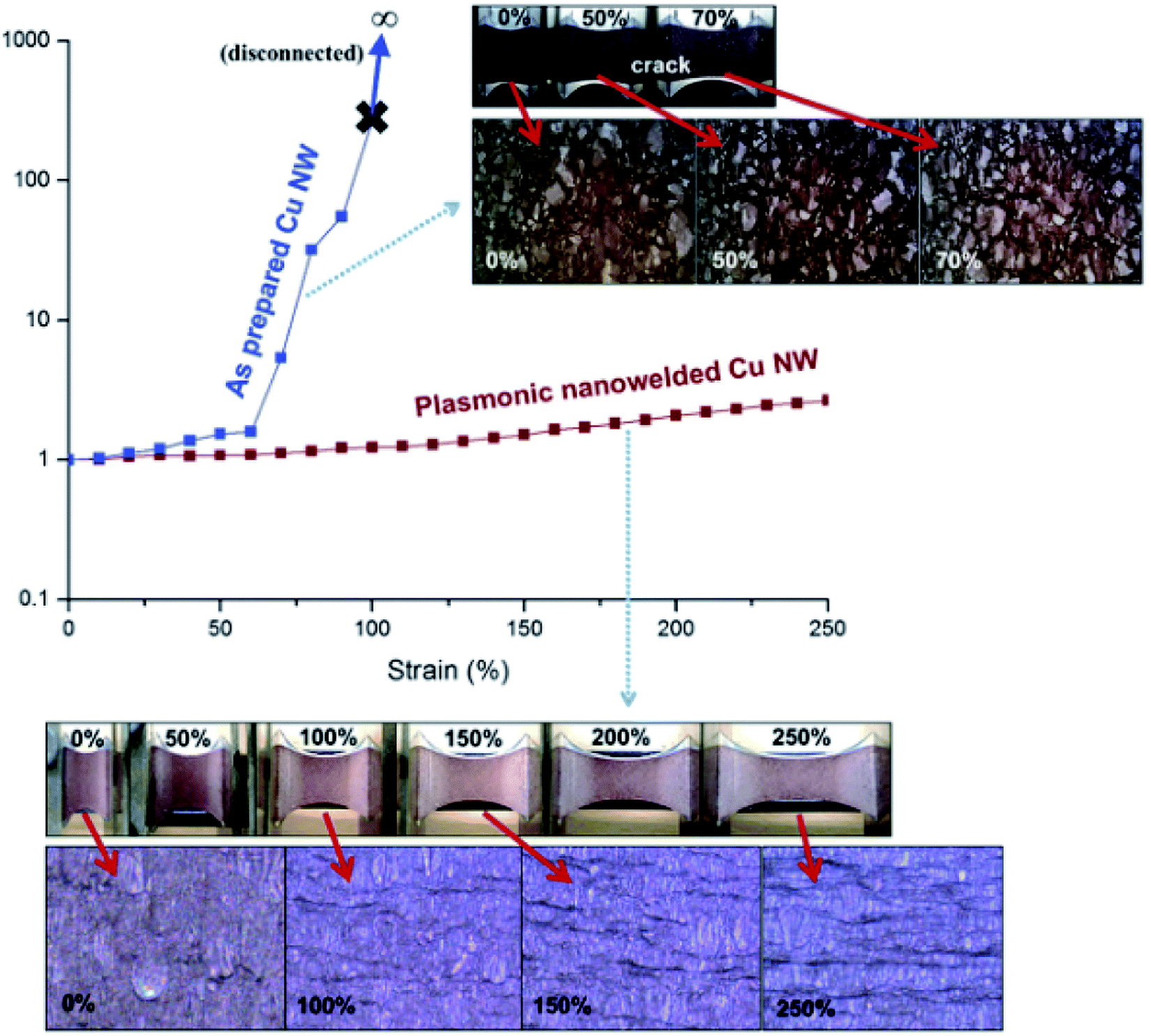 | ||
| Fig. 12 Resistance change of the simply coated and laser-nanowelded Cu NW electrodes at different strains. Inset shows the corresponding optical images under various strains.106 | ||
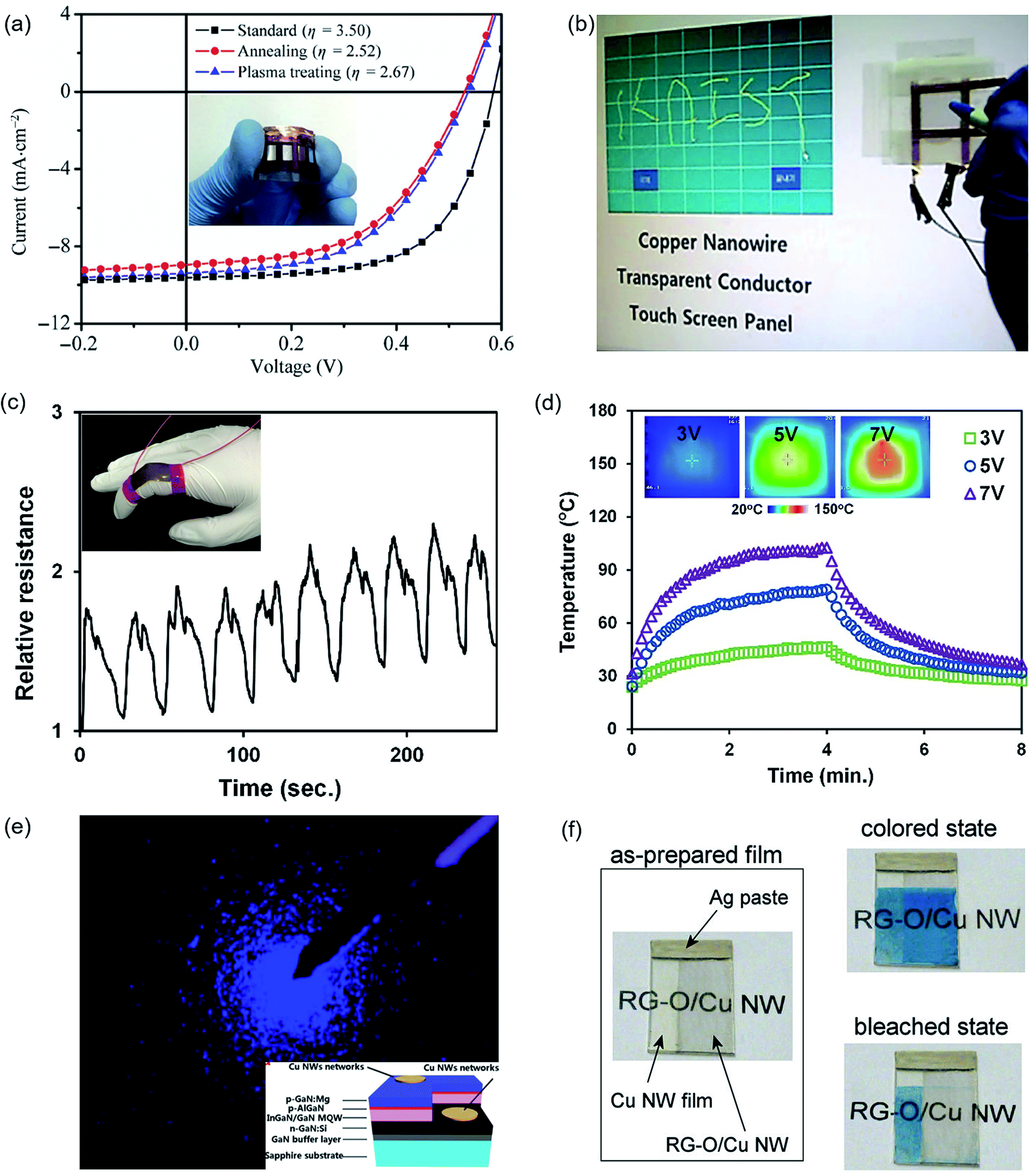 | ||
| Fig. 13 Applications of Cu NW TEs. (a) Characteristic I–V curves of solar cells with ITO or a Cu NW film as the transparent electrode. The inset shows the photograph of a flexible solar cell.100 (b) Demonstration of a touch-screen panel fabricated with a laser-nanowelded Cu NW TE.106 (c) Application of Cu NW/PU conductors in a strain sensor recording the relative resistance response of Cu NW/PU conductors to the bending and releasing of a finger.108 (d) Temperature profiles as a function of applied voltage of 3, 5, and 7 V on the Cu NW/PU heater. (e) Optical image of the blue light electroluminescence of an InGaN-based LED with Cu NW TEs.95 (f) An as-prepared mixed transparent electrode composed of a pure Cu NW film (left) and RGO/Cu NW film (right). The initial (coloured) state (right-top) and bleached state (right-bottom) of PB deposited on the mixed electrode.128 | ||
Polymer solar cells have evolved as promising cost-effective alternatives to silicon-based solar cells. The so-called plastic solar cells have important advantages, including a low cost, mechanical flexibility and versatility of chemical structures.137 However, the normally used ITO for the anode is expensive and fragile, which is not proper for flexible solar cells. Due to the excellent electrical and optical performances, Cu NW TEs are competitive candidates to replace ITO electrodes in solar cells. The protection of the Cu NW network from oxidation is also an essential issue for the integration of Cu NW TEs in solar cells. Thus, the Cu NW TEs are always used after post-treatment of coating passivation layers. To make solar cells using Cu NW TEs, a thin layer of TiO2 nanoparticles was spin coated as an electron transfer layer as well as a protection layer and followed by the casting of the photoactive layer (P3HT:PCBM) in a glove-box.116 Fig. 13(a) shows a photograph and the current–voltage (I–V) curve for the as-prepared flexible film solar cell solar cells using a Cu NW films as the TE. The power conversion efficiency (PCE) was 2.67%, which was slightly smaller than that utilizing ITO possibly due to the large surface roughness of Cu NW TEs. To reduce the surface roughness, a thin 40 nm PEDOT:PSS layer was applied by spin coating. After coating the planarization layer, an F4ZnPc:C60 heterojunction cell was deposited on the PEDOT:PSS-coated Cu NW TE. The PCE of the Cu NW solar cell was 3.1% which is comparable to the 4.0% for ITO.100 However, the acidic property of PEDOT:PSS caused a corrosive environment for the Cu NWs, resulting in reduced electrical properties. Graphene was used to enhance the chemical stability of the Cu NW TEs and showed excellent resistance against acidic corrosion. The solar cell using the Cu NW–graphene TE exhibited a PCE of 4.04%.130 Based on these results, Cu NW TEs could be used as a suitable replacement for ITO in low-cost and flexible solar cells. Modifying the surface morphology and improving the electrical properties of Cu NW TEs could further improve the performance of solar cells.
The electronics that operate through touch screens are rapidly growing and providing important opportunities for Cu NW TEs. The expensive and supply limited ITO could not satisfy the large demand for low-cost touch modules. Solution-processed Cu NW TEs supply one way to lower the cost and provide more possibility for flexible electronics. Han et al.106 fabricated a touch screen panel using Cu NW TEs made with the laser nanowelding method, as shown in Fig. 13(b). The letters “KAIST” were displayed on the screen by writing on the Cu NW touch screen. Chu et al.9 assembled Cu NW TEs as large-scale resistive touch screens to turn on various devices, such as LEDs, speakers and so on, indicating that Cu NW TE touch screens have potential to be applied in devices of various sizes.
Ding et al.108 reported the fabrication of a wearable sensor and heater by photonic sintered Cu NW/PU stretchable electrodes. The gesture of a finger attached to a Cu NW/PU electrode could be detected by the electrical signal, as drawn in Fig. 13(c). The result implied that the Cu NW/PU electrode could be used as an e-skin to characterize the gesture of fingers or joints. Jason et al.138 fabricated highly sensitive strain sensors by Cu NW and graphite microflakes for biomedical monitoring, including the skin over arteries, muscles and joints. The composite network was painted directly on the inner wrist to detect each finger's movement, palm flexion and extension. A sock with the hybrid composite painted on was designed to monitor the ankle movement during sporting actions in real time. The facial fabrication route and sensitivity of the Cu NW and graphite conductive composite made it ideal for healthcare and movement monitor.
Thanks to the excellent electrical conductivity, this Cu NW/PU electrode was used as a heater, and the surface temperature at different voltages was recorded (Fig. 13(d)). The temperature of the Cu NW/PU heater could reach 46 °C when a small voltage of 3 V was inputted, which was high enough to keep hands warm during a cold winter. Moon's group111 fabricated transparent conductive heaters using patterned Cu NW TEs and examined stability of the heater under mechanical deformation. The results confirmed that the heater was highly stable with a low deviation (±1 °C) under bending stress with a radii from 10 to 30 mm. Zhang et al.139 made stretchable heater based on Cu@Ag core–shell nanowire TEs using the one-step photonic sintering method. Owing to the Ag shells and the embedded structure caused by the photonic process, the heaters have a wide outputting temperature range (up to 130 °C when the input voltage was 6 V) and show excellent thermal stability. Remarkably, the temperature on the heater (with 80% transmittance) was 62 °C when gradually stretched up to 60%.
The applications of Cu NW TEs in other devices have also been demonstrated. The Cu NW TEs were also made as contact electrodes in GaN-based blue LED units, and the bright electroluminescence was achieved through the excellent transparency of the Cu NW TEs (Fig. 13(e)).95 Kholmanov et al.128 reported the application of Cu NW TEs with RGO protection in Prussian blue (PB)-based electrochromic devices (Fig. 13(f)). The corrosive solution would easily destroy bare Cu NW TEs, while the RGO layer perfectly protected the Cu NWs. Thus, in the electrochemical bleaching processes, the PB layers on top of the RGO/CU NW TEs were bleached, while in comparison, no bleaching of the PB layer on the pure Cu NW TEs was observed due to the decline in conductivity.
From the above, Cu NW TEs have been applied in various devices in the laboratory, mainly depending on both the high conductivity and the high optical transmittance. In some conditions, the Cu NW TEs should be carefully protected from corrosion, avoiding the decline or failure of conductivity. On the other hand, the stability of Cu NW TEs should also be considered for the long-term operation of devices.
6 Conclusions and outlook
Cu NW TE represents one of the most promising alternatives to ITO because of its low-cost solution processing, excellent optoelectronic performance and mechanical flexibility. The feasibility of scalable solution-fabrication processes could dramatically reduce the cost of Cu NW TEs, impelling their further application in thin-film solar cells, touch screens, heaters, LEDs and so on.We have reviewed the production of high-quality Cu NWs by solution-based techniques, including the hydrothermal route, hydrazine method, and catalytic method, which are considered to be facile, scalable strategies to synthesize Cu NWs. Furthermore, various techniques to generate Cu NW TEs have been highlighted for their fabrication processing, mechanism for conductivity improvement, and strategy for oxidation-resistant Cu NWs as well as their advantages in practical production. An overview of the protection methods for easily oxidized Cu NW networks have been given, and different kinds of passivation layers coating on individual Cu NW or on the whole network have been demonstrated. At last, the general applications of Cu NW TEs have been presented with examples to accentuate their growing interest and rapid development.
Despite the various fabrication methods and applications of Cu NW TEs that have been reported, some issues remain to be addressed before industrial production. Continuing efforts are required to develop large-scale production techniques for highly conductive Cu NW TEs on various substrates, avoiding the oxidation issue as well as forming nanojunctions between nanowires. Furthermore, the long-term stability of as-fabricated Cu NW TEs should be systematically studied and the ideal protection strategy for a low cost should be updated. The mechanical properties (such as bending, folding, and stretching) of Cu NW TEs on flexible substrates should be investigated to advance and realize future electronics that can provide more convenience to people, for example, bending a screen to attach to an arm or folding an e-paper to easily put in a pocket. Further study is needed to solve these problems and to realize the application of Cu NW TEs in phones and computers, which are used in our daily life.
Conflicts of interest
There are no conflicts to declare.Acknowledgements
The authors are thankful for the financial support from National Natural Science Foundation of China (Grant No. 51522503) and support from Program for New Century Excellent Talents in University (NCET-13-0175). The authors are also grateful for financial support from the National Natural Science Foundation of China (Grant No. 51705115).References
- Y. H. Kim, J. Lee, S. Hofmann, M. C. Gather, L. Müller-Meskamp and K. Leo, Adv. Funct. Mater., 2013, 23, 3763–3769 CrossRef CAS.
- N. Li, S. Oida, G. S. Tulevski, S. J. Han, J. B. Hannon, D. K. Sadana and T. C. Chen, Nat. Commun., 2013, 4, 2294 CrossRef PubMed.
- J. Tae Lim, H. Lee, H. Cho, B. H. Kwon, N. Sung Cho, B. Kuk Lee, J. Park, J. Kim, J. H. Han, J. H. Yang, B. G. Yu, C. S. Hwang, S. Chu Lim and J. I. Lee, Sci. Rep., 2015, 5, 17748 CrossRef CAS PubMed.
- S. Naghdi, K. Rhee, D. Hui and S. Park, Coatings, 2018, 8, 278 CrossRef.
- Y. Huang, Z. Huang, Z. Zhong, X. Yang, Q. Hong, H. Wang, S. Huang, N. Gao, X. Chen, D. Cai and J. Kang, Sci. Rep., 2018, 8, 13721 CrossRef PubMed.
- A. R. Madaria, A. Kumar and C. Zhou, Nanotechnology, 2011, 22, 245201 CrossRef PubMed.
- S. Gong, Y. Zhao, L. W. Yap, Q. Shi, Y. Wang, J. A. P. B. Bay, D. T. H. Lai, H. Uddin and W. Cheng, Adv. Electron. Mater., 2016, 2, 1600121 CrossRef.
- S. Bae, H. Kim, Y. Lee, X. Xu, J. S. Park, Y. Zheng, J. Balakrishnan, T. Lei, H. R. Kim, Y. I. Song, Y. J. Kim, K. S. Kim, B. Ozyilmaz, J. H. Ahn, B. H. Hong and S. Iijima, Nat. Nanotechnol., 2010, 5, 574–578 CrossRef CAS PubMed.
- H. C. Chu, Y. C. Chang, Y. Lin, S. H. Chang, W. C. Chang, G. A. Li and H. Y. Tuan, ACS Appl. Mater. Interfaces, 2016, 8, 13009–13017 CrossRef CAS PubMed.
- T. Tokuno, M. Nogi, M. Karakawa, J. Jiu, T. T. Nge, Y. Aso and K. Suganuma, Nano Res., 2011, 4, 1215–1222 CrossRef CAS.
- M. W. Rowell, M. A. Topinka, M. D. McGehee, H. J. Prall, G. Dennler, N. S. Sariciftci, L. Hu and G. Gruner, Appl. Phys. Lett., 2006, 88, 233506 CrossRef.
- X. Wang, L. Zhi and K. Müllen, Nano Lett., 2008, 8, 323–327 CrossRef CAS PubMed.
- H. Hwang, A. Kim, Z. Zhong, H.-C. Kwon, S. Jeong and J. Moon, Adv. Funct. Mater., 2016, 26, 6545–6554 CrossRef CAS.
- Y. R. Jang, W. H. Chung, Y. T. Hwang, H. J. Hwang, S. H. Kim and H. S. Kim, ACS Appl. Mater. Interfaces, 2018, 10, 24099–24107 CrossRef CAS PubMed.
- D. J. Lipomi, M. Vosgueritchian, B. C. Tee, S. L. Hellstrom, J. A. Lee, C. H. Fox and Z. Bao, Nat. Nanotechnol., 2011, 6, 788–792 CrossRef CAS PubMed.
- Y. Zhang, J. Guo, D. Xu, Y. Sun and F. Yan, Langmuir, 2018, 34, 3884–3893 CrossRef CAS PubMed.
- I. Hong, S. Lee, D. Kim, H. Cho, Y. Roh, H. An, S. Hong, S. H. Ko and S. Han, Nanotechnology, 2019, 30, 074001 CrossRef CAS PubMed.
- D. Kim, J. Kwon, J. Jung, K. Kin, H. Lee, J. Yeo, S. Hong, S. Han and S. H. Ko, Small Methods, 2018, 2, 1800077 CrossRef.
- J. Xue, J. Chen, J. Song, L. Xu and H. Zeng, J. Mater. Chem. C, 2017, 5, 11018–11024 RSC.
- S. Jung, K. Lim, J. W. Kang, J. K. Kim, S. I. Oh, K. Eun, D. G. Kim and S. H. Choa, Thin Solid Films, 2014, 550, 435–443 CrossRef CAS.
- J. Y. Lee, S. T. Connor, Y. Cui and P. Peumans, Nano Lett., 2008, 8, 689–692 CrossRef CAS PubMed.
- H. G. Im, S. H. Jung, J. Jin, D. Lee, J. Lee, D. Lee, J. Y. Lee, I. D. Kim and B. S. Bae, ACS Nano, 2014, 8, 10973–10979 CrossRef CAS PubMed.
- M. G. Kang, H. J. Park, S. H. Ahn and L. J. Guo, Sol. Energy Mater. Sol. Cells, 2010, 94, 1179–1184 CrossRef CAS.
- H. G. Im, B. W. An, J. Jin, J. Jang, Y. G. Park, J. U. Park and B. S. Bae, Nanoscale, 2016, 8, 3916–3922 RSC.
- B. W. An, E. J. Gwak, K. Kim, Y. C. Kim, J. Jang, J. Y. Kim and J. U. Park, Nano Lett., 2016, 16, 471–478 CrossRef CAS PubMed.
- D. S. Hecht, L. Hu and G. Irvin, Adv. Mater., 2011, 23, 1482–1513 CrossRef CAS PubMed.
- S. Ye, A. R. Rathmell, Z. Chen, I. E. Stewart and B. J. Wiley, Adv. Mater., 2014, 26, 6670–6687 CrossRef CAS PubMed.
- L. Hu, H. S. Kim, J.-Y. Lee, P. Peumans and Y. Cui, ACS Nano, 2010, 4, 2955–2963 CrossRef CAS PubMed.
- J. Lee, P. Lee, H. Lee, D. Lee, S. S. Lee and S. H. Ko, Nanoscale, 2012, 4, 6408–6414 RSC.
- U. Wang, J. Jiu, T. Araki, M. Nogi, T. Sugahara, S. Nagao, H. Koga, P. He and K. Suganuma, Nano-Micro Lett., 2015, 7, 51–58 CrossRef PubMed.
- H. Eom, J. Lee, A. Pichitpajongkit, M. Amjadi, J. H. Jeong, E. Lee, J. Y. Lee and I. Park, Small, 2014, 10, 4171–4181 CAS.
- T. B. Song, Y. S. Rim, F. Liu, B. Bob, S. Ye, Y. T. Hsieh and Y. Yang, ACS Appl. Mater. Interfaces, 2015, 7, 24601–24607 CrossRef CAS PubMed.
- H. H. Khaligh and I. A. Goldthorpe, Nanoscale Res. Lett., 2013, 8, 235 CrossRef PubMed.
- F. N. Kholid, H. Huang, Y. Zhang and H. J. Fan, Nanotechnology, 2016, 27, 025703 CrossRef PubMed.
- T. B. Song, Y. Chen, C. H. Chung, Y. M. Yang, B. Bob, H. S. Duan, G. Li, K. N. Tu, Y. Huang and Y. Yang, ACS Nano, 2014, 8, 2804–2811 CrossRef CAS PubMed.
- A. R. Rathmell, S. M. Bergin, Y. L. Hua, Z. Y. Li and B. J. Wiley, Adv. Mater., 2010, 22, 3558–3563 CrossRef CAS PubMed.
- M. Vosgueritchian, D. J. Lipomi and Z. Bao, Adv. Funct. Mater., 2012, 22, 421–428 CrossRef CAS.
- K. Lim, S. Jung, J.-K. Kim, J. W. Kang, J. H. Kim, S. H. Choa and D. G. Kim, Sol. Energy Mater. Sol. Cells, 2013, 115, 71–78 CrossRef CAS.
- N. Fukaya, D. Y. Kim, S. Kishimoto, S. Noda and Y. Ohno, ACS Nano, 2014, 8, 3285–3293 CrossRef CAS PubMed.
- S. L. Hellstrom, H. W. Lee and Z. Bao, ACS Nano, 2009, 3, 1423–1430 CrossRef CAS PubMed.
- H. A. Becerril, J. Mao, Z. Liu, R. M. Stoltenberg, Z. Bao and Y. Chen, ACS Nano, 2008, 2, 463–470 CrossRef CAS PubMed.
- X. Li, Y. Zhu, W. Cai, M. Borysiak, B. Han, D. Chen, R. D. Piner, L. Colombo and R. S. Ruoff, Nano Lett., 2009, 9, 4359–4363 CrossRef CAS PubMed.
- X. Wang, L. Zhi and K. Müllen, Nano Lett., 2008, 8, 323–327 CrossRef CAS PubMed.
- M. Mohl, P. Pusztai, A. Kukovecz, Z. Konya, J. Kukkola, K. Kordas, R. Vajtai and P. M. Ajayan, Langmuir, 2010, 26, 16496–16502 CrossRef CAS PubMed.
- M. Jin, G. He, H. Zhang, J. Zeng, Z. Xie and Y. Xia, Angew. Chem., Int. Ed., 2011, 50, 10560–10564 CrossRef CAS PubMed.
- A. R. Madaria, A. Kumar, F. N. Ishikawa and C. Zhou, Nano Res., 2010, 3, 564–573 CrossRef CAS.
- S. De, T. M. Higgins, P. E. Lyons, E. M. Doherty, P. N. Nirmalraj, W. J. Blau, J. J. Boland and J. N. Coleman, ACS Nano, 2009, 3, 1767–1774 CrossRef CAS PubMed.
- Y. Won, A. Kim, D. Lee, W. Yang, K. Woo, S. Jeong and J. Moon, NPG Asia Mater., 2014, 6, e105 CrossRef CAS.
- S. Ding, J. Jiu, Y. Tian, T. Sugahara, S. Nagao and K. Suganuma, Phys. Chem. Chem. Phys., 2015, 17, 31110–31116 RSC.
- E. C. Garnett, W. Cai, J. J. Cha, F. Mahmood, S. T. Connor, M. Greyson Christoforo, Y. Cui, M. D. McGehee and M. L. Brongersma, Nat. Mater., 2012, 11, 241–249 CrossRef CAS PubMed.
- C. H. Liu and X. Yu, Nanoscale Res. Lett., 2011, 6, 75 CrossRef PubMed.
- A. R. Rathmell and B. J. Wiley, Adv. Mater., 2011, 23, 4798–4803 CrossRef CAS.
- J. H. Yoo, Y. Kim, M. K. Han, S. Choi, K. Y. Song, K. C. Chung, J. M. Kim and J. Kwak, ACS Appl. Mater. Interfaces, 2015, 7, 15928–15934 CrossRef CAS PubMed.
- S. M. Bergin, Y. H. Chen, A. R. Rathmell, P. Charbonneau, Z. Y. Li and B. J. Wiley, Nanoscale, 2012, 4, 1996–2004 RSC.
- J. W. Borchert, I. E. Stewart, S. Ye, A. R. Rathmell, B. J. Wiley and K. I. Winey, Nanoscale, 2015, 7, 14496–14504 RSC.
- E. Ye, S. Y. Zhang, S. Liu and M. Y. Han, Chemistry, 2011, 17, 3074–3077 CrossRef CAS PubMed.
- D. Langley, G. Giusti, C. Mayousse, C. Celle, D. Bellet and J.-P. Simonato, Nanotechnology, 2013, 24, 452001 CrossRef PubMed.
- J. Xue, J. Song, Y. Dong, L. Xu, J. Li and H. Zeng, Sci. Bull., 2017, 62, 143–156 CrossRef CAS.
- J. Son and H. Zeng, Angew. Chem., Int. Ed., 2015, 54, 9760–9774 CrossRef PubMed.
- S. Zhong, T. Koch, M. Wang, T. Scherer, S. Walheim, H. Hahn and T. Schimmel, Small, 2009, 5, 2265–2270 CrossRef CAS.
- C. Schmädicke, M. Poetschke, L. D. Renner, L. Baraban, M. Bobeth and G. Cuniberti, RSC Adv., 2014, 4, 46363–46368 RSC.
- P. C. Hsu, D. Kong, S. Wang, H. Wang, A. J. Welch, H. Wu and Y. Cui, J. Am. Chem. Soc., 2014, 136, 10593–10596 CrossRef CAS.
- L. Zaraska, G. D. Sulka and M. Jaskuła, Appl. Surf. Sci., 2012, 258, 7781–7786 CrossRef CAS.
- G. A. Gelves, Z. T. M. Murakami, M. J. Krantz and J. A. Haber, J. Mater. Chem., 2006, 16, 3075 RSC.
- M. Motoyama, Y. Fukunaka, T. Sakka, Y. H. Ogata and S. Kikuchi, J. Electroanal. Chem., 2005, 584, 84–91 CrossRef CAS.
- G. Song, X. Li, Y. Wang, Z. Peng, Y. Yu and P. Li, Mater. Charact., 2010, 61, 371–375 CrossRef CAS.
- H. Cao, L. Wang, Y. Qiu and L. Zhang, Nanotechnology, 2006, 17, 1736–1739 CrossRef CAS PubMed.
- X. Liu and Y. Zhou, J. Mater. Res., 2011, 20, 2371–2378 CrossRef.
- A. M. Stortini, L. M. Moretto, A. Mardegan, M. Ongaro and P. Ugo, Sens. Actuators, B, 2015, 207, 186–192 CrossRef CAS.
- Y. Konishi, M. Motoyama, H. Matsushima, Y. Fukunaka, R. Ishii and Y. Ito, J. Electroanal. Chem., 2003, 559, 149–153 CrossRef CAS.
- J. Pate, F. Zamora, S. M. D. Watson, N. G. Wright, B. R. Horrocks and A. Houlton, J. Mater. Chem. C, 2014, 2, 9265–9273 RSC.
- Y. Shi, H. Li, L. Chen and X. Huang, Sci. Technol. Adv. Mater., 2016, 6, 761–765 CrossRef.
- E. Y. Bol’shagin and V. I. Roldughin, Colloid J., 2012, 74, 649–654 CrossRef.
- Z. Qian and S. J. Park, Chem. Mater., 2014, 26, 6172–6177 CrossRef CAS.
- O. Krichevski, Y. Levi-Kalisman, D. Szwarcman, Y. Lereah and G. Markovich, J. Colloid Interface Sci., 2007, 314, 304–309 CrossRef CAS PubMed.
- S. Li, Y. Chen, L. Huang and D. Pan, Inorg. Chem., 2014, 53, 4440–4444 CrossRef CAS PubMed.
- D. V. Kumar, I. Kim, Z. Zhong, K. Kim, D. Lee and J. Moon, Phys. Chem. Chem. Phys., 2014, 16, 22107–22115 RSC.
- Z. Jiang, Y. Tian and S. Ding, Mater. Lett., 2014, 136, 310–313 CrossRef CAS.
- Y. Chang, M. L. Lye and H. C. Zeng, Langmuir, 2005, 21, 3746–3748 CrossRef CAS.
- S. Ye, A. R. Rathmell, I. E. Stewart, Y. C. Ha, A. R. Wilson, Z. Chen and B. J. Wiley, Chem. Commun., 2014, 50, 2562–2564 RSC.
- S. Ye, Z. Chen, Y. C. Ha and B. J. Wiley, Nano Lett., 2014, 14, 4671–4676 CrossRef CAS.
- S. Ye, A. R. Rathmell, Y. C. Ha, A. R. Wilson and B. J. Wiley, Small, 2014, 10, 1771–1778 CrossRef CAS PubMed.
- Y. Zheng, J. Liang, Y. Chen and Z. Liu, RSC Adv., 2014, 4, 41683–41689 RSC.
- S. Ye, I. E. Stewart, Z. Chen, B. Li, A. R. Rathmell and B. J. Wiley, Acc. Chem. Res., 2016, 49, 442–451 CrossRef CAS PubMed.
- M. Luo, A. Ruditskiy, H. C. Peng, J. Tao, L. Figueroa-Cosme, Z. He and Y. Xia, Adv. Funct. Mater., 2016, 26, 1209–1216 CrossRef CAS.
- D. Zhang, R. Wang, M. Wen, D. Weng, X. Cui, J. Sun, H. Li and Y. Lu, J. Am. Chem. Soc., 2012, 134, 14283–14286 CrossRef CAS PubMed.
- B. Jia, M. Qin, Z. Zhang, A. Chu, L. Zhang, Y. Liu and X. Qu, J. Mater. Sci., 2013, 48, 4073–4080 CrossRef CAS.
- H. J. Yang, S. Y. He and H. Y. Tuan, Langmuir, 2014, 30, 602–610 CrossRef CAS PubMed.
- Y. Q. Liu, M. Zhang, F. X. Wang and G. B. Pan, RSC Adv., 2012, 2, 11235–11237 RSC.
- S. Bhanushali, P. Ghosh, A. Ganesh and W. Cheng, Small, 2015, 11, 1232–1252 CrossRef CAS PubMed.
- F. Cui, Y. Yu, L. Dou, J. Sun, Q. Yang, C. Schildknecht, K. Schierle-Arndt and P. Yang, Nano Lett., 2015, 15, 7610–7615 CrossRef CAS PubMed.
- M. Kevin, G. Y. R. Lim and G. W. Ho, Green Chem., 2015, 17, 1120–1126 RSC.
- F. Meng and S. Jin, Nano Lett., 2012, 12, 234–239 CrossRef CAS.
- S. Alvarez, S. Ye, P. F. Flowers and B. J. Wiley, Chem. Mater., 2015, 27, 570–573 CrossRef CAS.
- H. Guo, N. Lin, Y. Chen, Z. Wang, Q. Xie, T. Zheng, N. Gao, S. Li, J. Kang, D. Cai and D. L. Peng, Sci. Rep., 2013, 3, 2323 CrossRef.
- R. Yuge, S. Bandow, M. Yudasaka, K. Toyama, S. Iijima and T. Manako, Carbon, 2017, 111, 675–680 CrossRef CAS.
- J. Lee, I. Lee, T. S. Kim and J. Y. Lee, Small, 2013, 9, 2887–2894 CrossRef CAS PubMed.
- C. Mayousse, C. Celle, A. Carella and J. P. Simonato, Nano Res., 2014, 7, 315–324 CrossRef CAS.
- L. Xu, Y. Yang, Z. W. Hu and S. H. Yu, ACS Nano, 2016, 10, 3823–3834 CrossRef CAS PubMed.
- C. Sachse, N. Weiß, N. Gaponik, L. Müller-Meskamp, A. Eychmüller and K. Leo, Adv. Energy Mater., 2014, 4, 1300737 CrossRef.
- H. Xu, H. Wang, C. Wu, N. Lin, A. M. Soomro, H. Guo, C. Liu, X. Yang, Y. Wu, D. Cai and J. Kang, Nanoscale, 2015, 7, 10613–10621 RSC.
- Z. Yin, S. K. Song, D. J. You, Y. Ko, S. Cho, J. Yoo, S. Y. Park, Y. Piao, S. T. Chang and Y. S. Kim, Small, 2015, 11, 4576–4583 CrossRef CAS PubMed.
- Y. Won, A. Kim, W. Yang, S. Jeong and J. Moon, NPG Asia Mater., 2014, 6, e132 CrossRef CAS.
- I. E. Stewart, A. R. Rathmell, L. Yan, S. Ye, P. F. Flowers, W. You and B. J. Wiley, Nanoscale, 2014, 6, 5980–5988 RSC.
- C. R. Chu, C. Lee, J. Koo and H. M. Lee, Nano Res., 2016, 7, 2162–2173 CrossRef.
- S. Han, S. Hong, J. Ham, J. Yeo, J. Lee, B. Kang, P. Lee, J. Kwon, S. S. Lee, M. Y. Yang and S. H. Ko, Adv. Mater., 2014, 26, 5808–5814 CrossRef CAS.
- S. Han, S. Hong, J. Yeo, D. Kim, B. Kang, M. Y. Yang and S. H. Ko, Adv. Mater., 2015, 27, 6397–6403 CrossRef CAS.
- S. Ding, J. Jiu, Y. Gao, Y. Tian, T. Araki, T. Sugahara, S. Nagao, M. Nogi, H. Koga, K. Suganuma and H. Uchida, ACS Appl. Mater. Interfaces, 2016, 8, 6190–6199 CrossRef CAS.
- K. Mallikarjuna, H. J. Hwang, W. H. Chung and H.-S. Kim, RSC Adv., 2016, 6, 4770–4779 RSC.
- Z. Zhong, K. Woo, I. Kim, H. Hwang, S. Kwon, Y. M. Choi, Y. Lee, T. M. Lee, K. Kim and J. Moon, Nanoscale, 2016, 8, 8995–9003 RSC.
- Z. Zhong, H. Lee, D. Kang, S. Kwon, Y. M. Choi, I. Kim, K. Y. Kim, Y. Lee, K. Woo and J. Moon, ACS Nano, 2016, 10, 7847–7854 CrossRef CAS PubMed.
- J. H. Park, J. Seo, C. Kim, D. J. Joe, H. E. Lee, T. H. Im, J. Y. Seok, C. K. Jeong, B. S. Ma, H. K. Park, T. S. Kim and K. J. Lee, Adv. Sci., 2018, 5, 1801146 CrossRef PubMed.
- T. H. Im, D. Y. Park, H. K. Lee, J. H. Park, C. K. Jeong, D. J. Joe and K. J. Lee, Part. Part. Syst. Charact., 2017, 34, 1600429 CrossRef.
- J. H. Park, G. T. Hwang, S. Kim, J. Seo, H. J. Park, K. Yu, T. S. Kim and K. J. Lee, Adv. Mater., 2017, 29, 1603473 CrossRef.
- J. H. Park, S. Han, D. Kim, B. K. You, D. J. Joe, S. Hong, J. Seo, J. Kwon, C. K. Jeong, H. J. Park, T. S. Kim, S. H. Ko and K. J. Lee, Adv. Funct. Mater., 2017, 27, 1701138 CrossRef.
- R. Wang, H. Zhai, T. Wang, X. Wang, Y. Cheng, L. Shi and J. Sun, Nano Res., 2016, 9, 2138–2148 CrossRef CAS.
- B. Zhang, W. Li, J. Jiu, Y. Yang, J. Jing, K. Suganuma and C. Li, Inorg. Chem., 2019, 58, 3374–3381 CrossRef CAS.
- J. Xue, J. Song, Y. Zou, C. Huo, Y. Dong, L. Xu, J. Li and H. Zen, RSC Adv., 2016, 6, 91394–91400 RSC.
- S. Huang, Q. Zhang, P. Li, F. Ren, A. Yurtsever and D. Ma, Adv. Energy Mater., 2018, 8, 1703658 CrossRef.
- H. Zhai, R. Wang, X. Wang, Y. Cheng, L. Shi and J. Sun, Nano Res., 2016, 9, 3924–3936 CrossRef CAS.
- L. Lian, H. Wang, D. Dong and G. He, J. Mater. Chem. C, 2018, 6, 9158–9165 RSC.
- Y. Tang, H. Ruan, Z. Huang, D. Shi, H. Liu, S. Chen and J. Zhang, Nanotechnology, 2018, 29, 455706 CrossRef.
- C. Celle, A. Cabos, T. Fontecave, B. Laguitton, A. Benayad, L. Guettaz, N. Pélissier, V. H. Nguyen, D. Bellet, D. Muñoz-Rojas and J. P. Simonato, Nanotechnology, 2018, 29, 085701 CrossRef.
- A. R. Rathmell, M. Nguyen, M. Chi and B. J. Wiley, Nano Lett., 2012, 12, 3193–3199 CrossRef CAS.
- J. Song, J. Li, J. Xu and H. Zeng, Nano Lett., 2014, 14, 6298–6305 CrossRef CAS.
- X. Wang, R. Wang, L. Shi and J. Sun, Small, 2015, 11, 4737–4744 CrossRef CAS.
- Po-C. Hsu, H. Wu, T. J. Carney, M. T. McDowell, Y. Yang, E. C. Garnett, M. Li, L. Hu and Y. Cui, ACS Nano, 2012, 6, 5150–5156 CrossRef CAS PubMed.
- I. N. Kholmanov, S. H. Domingues, H. Chou, X. Wang, C. Tan, J. Y. Kim, H. Li, R. Piner, A. J. G. Zarbin and R. S. Ruoff, ACS Nano, 2013, 7, 1811–1816 CrossRef CAS PubMed.
- L. Shi, R. Wang, H. Zhai, Y. Liu, L. Gao and J. Sun, Phys. Chem. Chem. Phys., 2015, 17, 4231–4236 RSC.
- Y. Ahn, Y. Jeong, D. Lee and Y. Lee, ACS Nano, 2015, 9, 3125–3133 CrossRef CAS PubMed.
- L. Dou, F. Cui, Y. Yu, G. Khanarian, S. W. Eaton, Q. Yang, J. Resasco, C. Schildknecht, K. Schierle-Arndt and P. Yang, ACS Nano, 2016, 10, 2600–2606 CrossRef CAS.
- J. Chen, W. Zhou, J. Chen, Y. Fan, Z. Zhang, Z. Huang, X. Feng, B. Mi, Y. Ma and W. Huang, Nano Res., 2014, 8, 1017–1025 CrossRef.
- C. K. Jeong, J. Lee, S. Han, J. Ryu, G. T. Hwang, D. Y. Park, J. H. Park, S. S. Lee, M. Byun, S. H. Ko and K. J. Lee, Adv. Mater., 2015, 27, 2866–2875 CrossRef CAS PubMed.
- M. H. Seo, J. Y. Yoo, S. Y. Choi, J. S. Lee, K. W. Choi, C. K. Jeong, K. J. Lee and J. B. Yoon, ACS Nano, 2017, 11, 1520–1529 CrossRef CAS PubMed.
- S. Huang, Y. Liu, Y. Zhao, Z. Ren and C. F. Guo, Adv. Funct. Mater., 2018, 29, 1805924 CrossRef.
- W. Hu, R. Wang, Y. Lu and Q. Pei, J. Mater. Chem. C, 2014, 2, 1298–1305 RSC.
- G. Li, V. Shrotriya, J. Huang, Y. Yao, T. Moriarty, K. Emery and Y. Yang, Nat. Mater., 2005, 4, 864–868 CrossRef CAS.
- N. N. Jason, S. J. Wang and W. Cheng, Nanoscale, 2016, 8, 16596–16605 RSC.
- B. Zhang, W. Li, M. Nogi, C. Chen, Y. Yang, T. Sugahara, H. Koga and K. Suganuma, ACS Appl. Mater. Interfaces, 2019, 11, 18540–18547 CrossRef CAS PubMed.
| This journal is © The Royal Society of Chemistry 2019 |