
 Open Access Article
 This Open Access Article is licensed under a Creative Commons Attribution-Non Commercial 3.0 Unported Licence
Tensile mechanical performance of Ni–Co alloy nanowires by molecular dynamics simulation
Xuefeng Lu *,
Panfeng Yang,
Jianhua Luo,
Junqiang Ren,
Hongtao Xue and
Yutian Ding
*,
Panfeng Yang,
Jianhua Luo,
Junqiang Ren,
Hongtao Xue and
Yutian Ding
State Key Laboratory of Advanced Processing and Recycling of Non-ferrous Metal, Department of Materials Science and Engineering, Lanzhou University of Technology, Lanzhou 730050, PR China. E-mail: luxuefeng1979@163.com
First published on 19th August 2019
Abstract
In this present contribution, tensile mechanical properties of Ni–Co alloy nanowires with Co content from 0 to 20% were studied by molecular dynamics. The simulation results show the alloy nanowire with the Co content of 5% has the highest yield value of 9.72 GPa. In addition, more Frank dislocations were generated during the loading process to improve the performance of the alloy nanowire. The Young's modulus increases little by little from 105.68 to 179.78 GPa with the increase of Co content. Secondly, with the increase of temperature, the yield strength gradually decreases to 2.13 GPa. Young's modulus tends to decrease linearly from 170.7 GPa to 48.21 GPa. At the temperatures of 500 K and 700 K, it is easier to form Frank dislocation and Hirth dislocation, respectively, in the loading process. The peak value of the radial distribution function decreases and the number of peaks decreases, indicating the disappearance of the ordered structure. Finally, after the introduction of the surface and inner void, the yield strength of the nanowire drops about to 8.97 and 6.6 GPa, respectively, and the yield strains drop to 0.056 and 0.043. In the case of the existence of internal void, perfect dislocation and Hirth dislocation can be observed in the structure.
Introduction
In recent years, with the improvement of material preparation technology and the change of material application requirements, the performance of single pure metal Ni and Co cannot meet the service requirements of materials in harsh environments. At present, because of its high hardness, good wear resistance, corrosion resistance, high temperature resistance and magnetism,1–5 Ni–Co alloy has received extensive attention in a variety of fields with regards to coating materials, magnetic materials and absorbing materials. The main methods for the preparation of Ni–Co alloy include co-deposition,6 electrodeposition,7 template method,8,9 liquid phase reduction method,10 sol–gel method,11 et al. The products with excellent performance are mainly obtained by adjusting the composition ratio and changing the experimental conditions. You et al.12 prepared Ni–Co alloy films by electrodeposition at room temperature, and found that the deposited films had a face-centered cubic structure and grain refinement. Maaz et al.13 prepared core and shell nanowires with fcc-Ni as the core and hcp-Co as the shell through experiments, and found that the saturation magnetization increased with the decrease of temperature. Akbarzadeh et al.14 used molecular dynamics to conduct a thermal analysis on the nanoclusters of Ni–Co alloy, and found that the increase of Ni content could improve the thermodynamic stability of the structure. The study of Ni–Co alloy nanostructures has become an important research issue because of unique and fascinating properties. Although the experimental research of Ni–Co alloy has already had a certain basis, the development of alloy materials requires a deeper understanding of the relationship between structure and properties at the atomic level.Compared with traditional bulk materials, metal nanostructured materials have some specific properties and effects, and have been widely used in nano-electronic devices. Moreover, the thermal and mechanical behaviors of nanostructured materials have an important impact on the usability and reliability of related nano-devices.15–17 The researchers experimentally prepared nanocrystalline Ni–Co alloys with different grain sizes and Co content, and found that the addition of Co increased strain hardening capacity and plasticity. Moreover, it was realized that the tensile strength and elongation to failure of the alloy increased to some extent when FCC and HCP phase were mainly in the alloy.18 Yang19 found that with lowering stacking fault energy, both the planar slip mode and the increased twinnability enhance the strain-hardening capability of the superalloy, which postpones the initiation of necking. Thus, the Synchronous improvement of strength and plasticity in the double-phase superalloy is achieved. Qin20 prepared Ni–Co alloy by electrodeposition method and found that the grain refinement, solid-solution hardening and decrease of stacking fault energy, which are caused by alloying of Co element, should be responsible for the excellent mechanical performance. Therefore, it is of great significance to study the mechanical performance of Ni–Co alloy nanostructures and explore its better properties and wider applications.
In the present contribution, the tensile behavior of Ni–Co alloy nanowires is investigated by molecular dynamics. Simultaneously, the influences of Co content, temperature and vacancy defects on the properties of Ni–Co alloy nanowires are analyzed as well as the structural transformation and internal deformation mechanism in the process of external loading.
Simulation details
We refer to the modeling method adopted by Mojumder to study the mechanical properties of Al–Cu alloy.21 The Ni–Co alloy nanowires are obtained by randomly adding some Co atoms to the Ni nanowires, as shown in Fig. 1. A replacement solid solution can be got by Co atoms serving as a substitute for Ni atoms. In the simulation system, the free boundary conditions are employed in three axial directions. In order to obtain a stable initial structure, the steepest descent algorithm is utilized to minimize energy before applying an external loading. Canonical ensemble (NVT) is used throughout the simulation process with an integration time step of 1 fs. The simulation system is controlled at 300 K by the Nose–Hoover temperature controller for 50 ps and the damping constant is set to 0.1. Some atoms at both ends are fixed along the Z-axis and then external loads were applied, and the loading speed is set at 0.02 Å ps−1. The X, Y, and Z axes correspond to [100], [010], and [001] crystal orientations, and the size of the model is 24.64 × 24.64 × 197.12 Å3. The aspect ratio of nanowire is 8![[thin space (1/6-em)]](https://www.rsc.org/images/entities/char_2009.gif) :1 and the atom number of system is 12713.
:1 and the atom number of system is 12713.
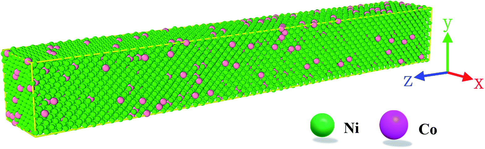 | ||
| Fig. 1 The simulation Ni–Co alloy nanowire configuration. Ni: green; Co: pink atoms. | ||
Here the MD simulations are carried out using the large-scale atomic/molecular massively parallel simulator (LAMMPS).22 All simulations used the EAM (Embedded Atomic Method) potential23 to describe the interactions between atoms in the system, which has been shown to be correct in the Ni–Co system.23,24 In the EAM,25 The total energy Ei of an atom i is represented by:
 | (1) |
The host electron density is given by:
 | (2) |
The details of the parameters are shown in Table 1. Refer to ref. 23, 26 and 27 for details on potential function construction. Atomeye28 is used to visualize atomic motion trajectories and atomic configuration analysis was performed by Ovito software.29 The structural transformation of the nanowires after deformation is analyzed by the Common Neighbor Analysis (CNA).30,31 The dislocation changes during loading were analyzed by DXA (Dislocation Extraction Algorithm).32
| Parameter | Value |
|---|---|
| rc (nm) | 0.62958 |
| h (nm) | 3.3816 × 10⁻² |
| E0 (eV) | 0.18136 |
| r1 (nm) | 0.2829 |
| b1 | 2.1236 |
| Q | 1.5906 |
| δ (eV) | −3.594 × 10⁻² |
| sNi | 0.6816 |
| sCo | 1.0000 |
| gCo (eV) | 0.16643 |
| gNi (eV) | 0.9294 |
Results and discussions
Effect of Co content on tensile mechanical performance of Ni–Co alloy nanowire
For the purpose of investigating the mechanical performance and the fundamental deformation mechanism, the stress–strain curves are illustrated in Fig. 2 with the Co atom content from 0 to 20% at random position of nanowires. The tensile stresses increase gradually with the addition of Co elements for the Ni–Co alloy nanowires. The stresses of nanowires increase with the increasing of strains and then drop when the yield behavior occurred, as shown in Fig. 2a. In contrast, the yield strains of the materials after alloying decrease, which values are lower than that of pure Ni nanowire of 0.073. The alloy nanowire with the Co content of 5% has the highest yield value of 9.72 GPa (as illustrated in Fig. 2b). Accompanying the increase of Co content, the Young's modulus increases little by little from 105.68 to 179.78 GPa, demonstrated in Fig. 2c. Fig. 2d shows the potential evolution with the change of strain, it is found that after alloying the potential energies of materials with different Co content increase compared to pure Ni metal. On the one hand, the replacement of Co in the crystal lattice of Ni results in lattice distortion and hinders dislocation movement. Also, the addition of Co reduces the stacking fault energy of the material. Above all, after the addition of Co, the internal energy increases and high resistance to external forces is obtained, which are conducive to the potential applications in fields of aeroengine and energy devices.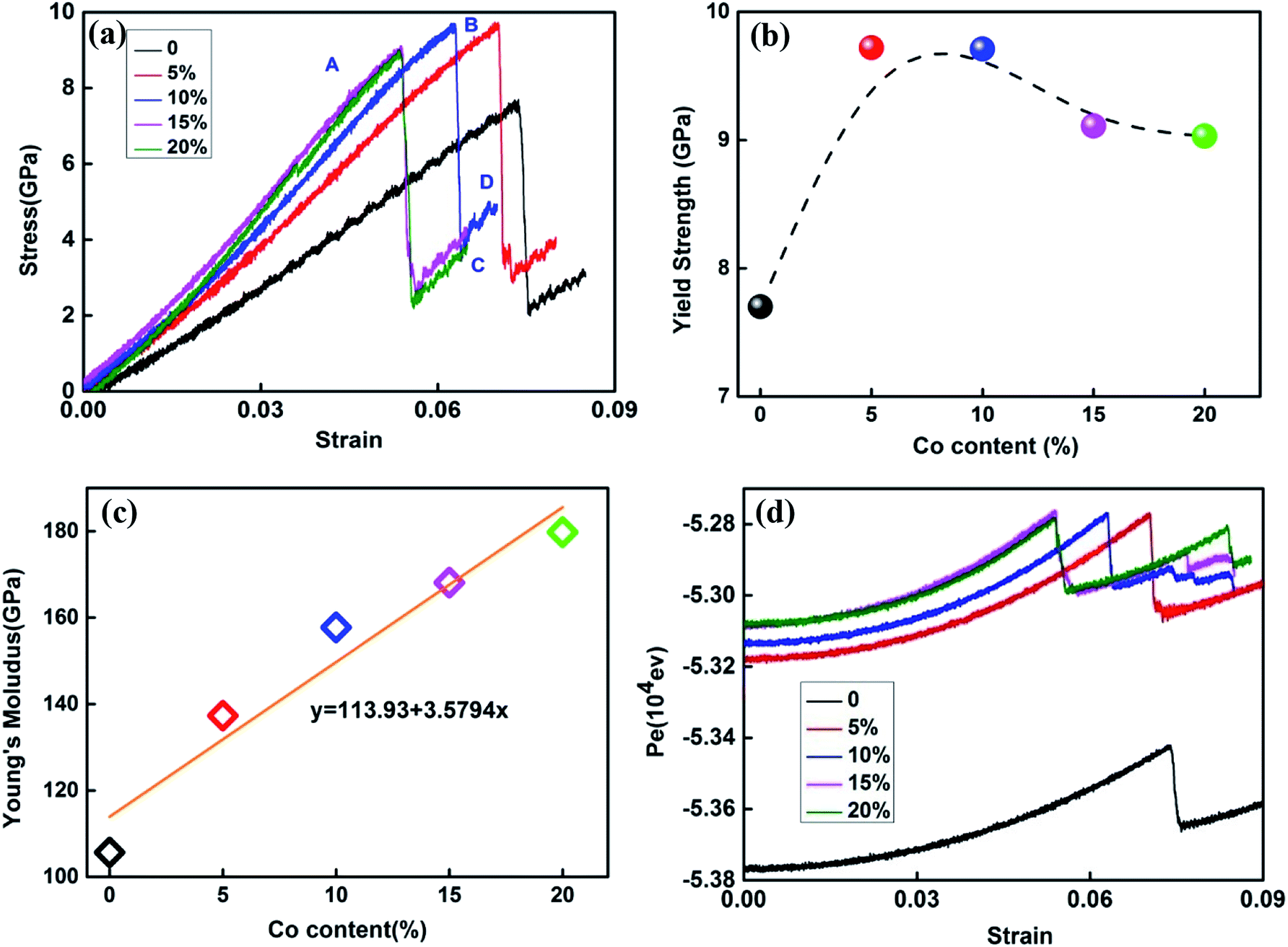 | ||
| Fig. 2 (a) Stress–strain curves of Ni–Co alloy nanowires. (b) Yield strength of alloy with different Co content. (c) Young's modulus of alloy with different Co content. (d) Potential energies of Ni–Co alloy nanowires. | ||
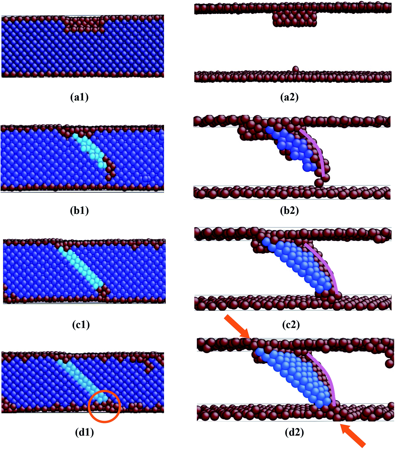
In order to clear the internal configuration evolution, the middle region of nanowire is magnified. As shown in Fig. 3(a1)–(d1), the structure includes red surface atoms, the concentrated area of light blue atoms is stacking fault, and the dark blue atoms represent perfect FCC lattice atoms. Fig. 3(a2)–(d2) shows the removal of perfect FCC lattice atoms by CNA method, leaving surface atoms, stacking fault, disordered atoms and dislocations. Fig. 3a is the state of nanowires with a Co content of 10% before yield. When the strain comes to 0.0627, the yield behavior of nanowires occurs when the dislocation occurs (as described by the arc purple line) and starts to move, as shown in Fig. 3b. Meanwhile, stacking fault caused by dislocation movement can be observed, as demonstrated by blue atoms. At strain of 0.064 (Fig. 3c), the stacking fault has accumulated with the extension of dislocation. It is found that in the process of loading, the dislocation moves to the surface of the nanowire and disappears, leaving steps (two oval line) on the top and bottom surfaces of the nanowire. The generated steps can be used as the dislocation source to continue transmitting the dislocation. As the dislocation moves (the arc red line), a certain number of stacking faults atoms are shown. In Fig. 3d, as the deformation progresses, hcp crystal structure composed of perfect stacking faults (light blue atoms) can be seen.
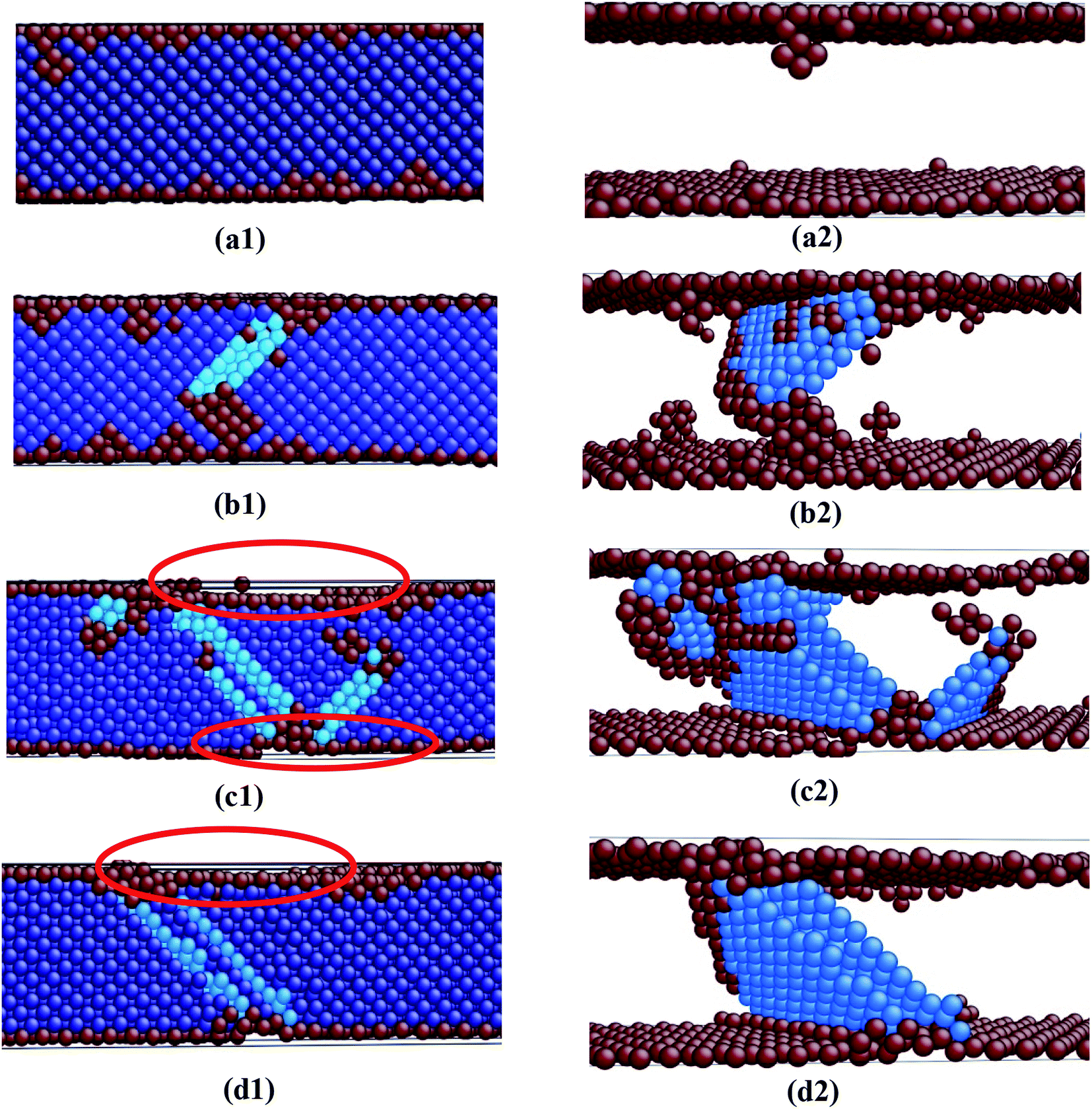 | ||
| Fig. 3 The deformation process of Ni–Co alloy nanowires with a Co content of 10% and an aspect ratio of 8:1 under tensile loading with different strains: (a) 0.0478; (b) 0.0627; (c) 0.064; (d) 0.07. | ||
It can be seen from Fig. 4 that, according to the DXA analysis results, the dislocation line length firstly increases and then decreases during the loading process. It can be seen that compared to the other components, the generated dislocation length of alloy nanowires with Co content of 5% is relatively the largest in the process of loading. Firstly, the introduction of Co element reduces the stacking fault energy of the material, leading to the reduction of the stress required for dislocation formation in the loading.
 | ||
| Fig. 4 The relationship between dislocation line length and strain in alloy nanowires with different Co content under tensile loading. | ||
Therefore, when the Co content is 5%, the nucleation of dislocation becomes easier and the length of dislocation line generated in the loading process significantly increases. However, the large amount of Co element will prevent the formation and expansion of dislocation, and subsequently it is found that when the Co content is more than 10%, the obstruction effect is particularly obvious.
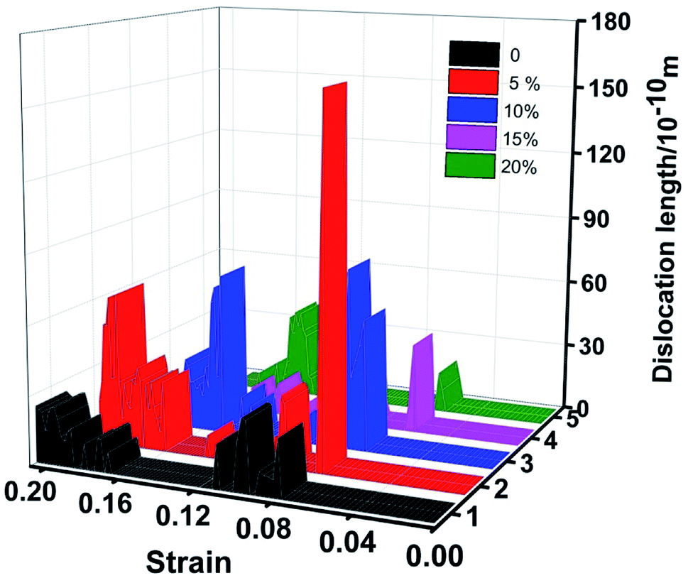
Because the lattice distortion caused by the addition of Co atoms and the reduction of the stacking fault energy of the system are of great help to the formation of dislocation, the length of dislocation line increases obviously. The increase of dislocation density improves the work hardening ability of nanowires, leading to the increase of strength. As the system is small, the dislocation line length in the structure is short, so the reaction between dislocations is weak. Shockley partial dislocation is usually the main part, and the mutual reaction between dislocations promotes the generation of other types of dislocations. The two Shockley dislocations intersect on the slip plane to generate stairs-rod dislocations. The generation of Frank dislocations can block the intersection of Shockley dislocations, resulting in the disappearance of the stair-rod dislocations. Fig. 5 shows the relationship between the strain and the length of different types of dislocation lines generated during the loading process. From the simulation results, different type of dislocations such as Frank, Shockley and stair-rod dislocation can be observed in the loading process under the conditions of different Co content. In Fig. 5a, Shockley dislocation and stair-rod dislocation formed in pure Ni system in the process of tensile loading, can be found. When the content of Co comes to 5%, the length of Shockley dislocation line in the structure increased and there exists a highest value of 140 Å, as shown in Fig. 5b. It is worth noting that stair-rod dislocation disappeared while Frank dislocation appeared in alloy nanowire. For Fig. 5c, the length of Shockley dislocation line in the nanowire decreases remarkably. At this time, Frank dislocation disappeared. However, stair-rod dislocation appeared again and there is a maximum value of 40 Å.
 | ||
| Fig. 5 Dislocation types and length changes in alloy nanowires with different Co content under tensile loading: (a) 0; (b) 5%; (c) 10%; (d) 15%; (e) 20%. | ||
As two common fixed dislocations in FCC structure, Frank dislocation and stair-rod dislocation hinder the movement of other dislocations to some extent,33,34 and thus show high yield strength in the stress–strain relationship, which is according with the results in Fig. 2a and b. With the continuous increase of Co content, the hinder extent derived from Co atoms in the formation and expansion of dislocation increases distinctly, resulting in the drop of the length of Shockley and stair-rod dislocation in Fig. 5d and e.
The experimental results of Xu et al.35 show that in nanocrystalline Ni–Co alloy when the Co content is lower than 15.4%, the tensile strength increases with the increase of Co content. Combined with the information shown in Fig. 2 in this paper, the yield strength of nanowires was higher when the Co content was 5% and 10%. Therefore, considering the two factors, we selected 10% Co alloy nanowires for further analysis of temperature and defect effects.
Effect of temperature on tensile mechanical performance of Ni–Co alloy nanowire
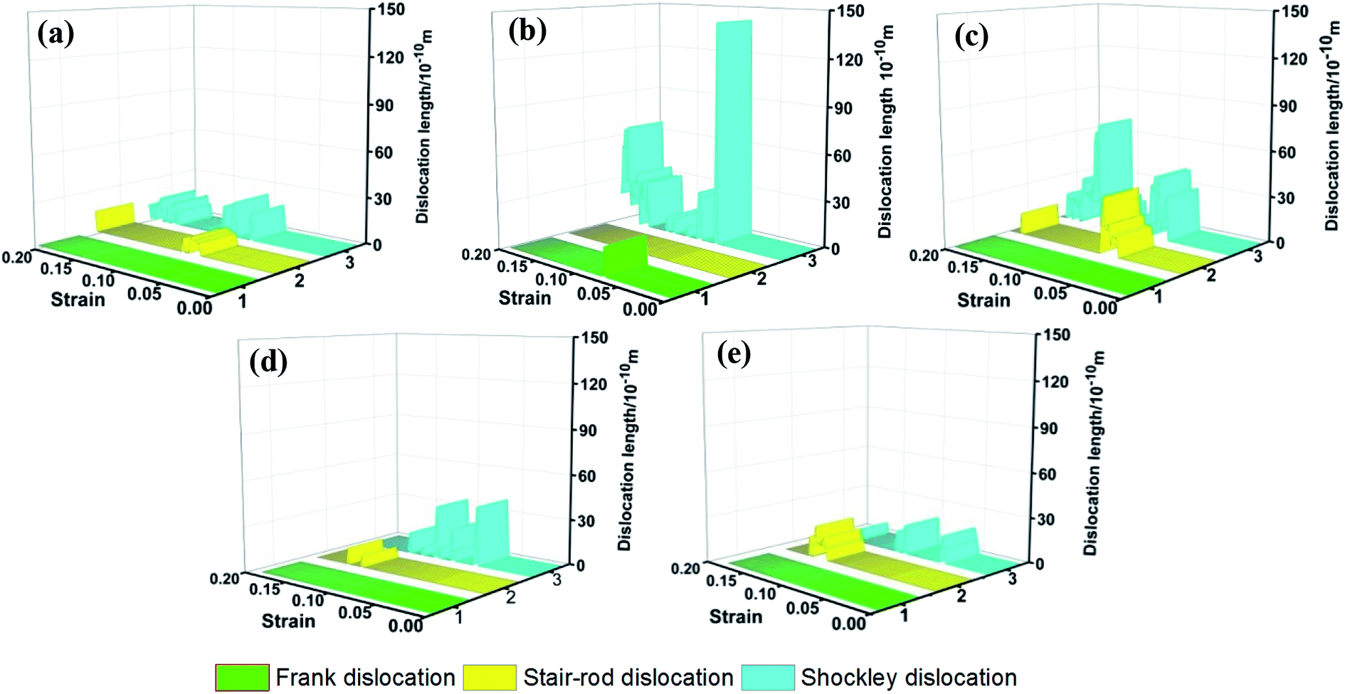
In order to study the influence of temperature on the loading process of Ni–Co alloy nanowires, the temperature range of 300K–1100 K was selected in this part to observe the deformation behavior of nanowires when the temperature increased. Fig. 6a is the stress–strain curve with the change of temperature factor. It can be seen that with the increase of temperature, the yield stress of the nanowire decreases obviously, and the yield strain also decreases remarkably. At the same time, it is found from Fig. 6b that the yield strength at 300 K has the highest value of 9.53 GPa. With the increase of temperature, the yield strength gradually decreases to 2.13 GPa. For Fig. 6c, it is found that with the increase of temperature, Young's modulus tends to decrease linearly from 170.7 to 48.21 GPa. Fig. 6d shows the radial distribution function of nanowires at different temperatures. At 300 K, the RDF peak value represents the ordered structure of nanowires. As the temperature rises, the peak value of the radial distribution function decreases and the number of peaks decreases, indicating the disappearance of the ordered structure.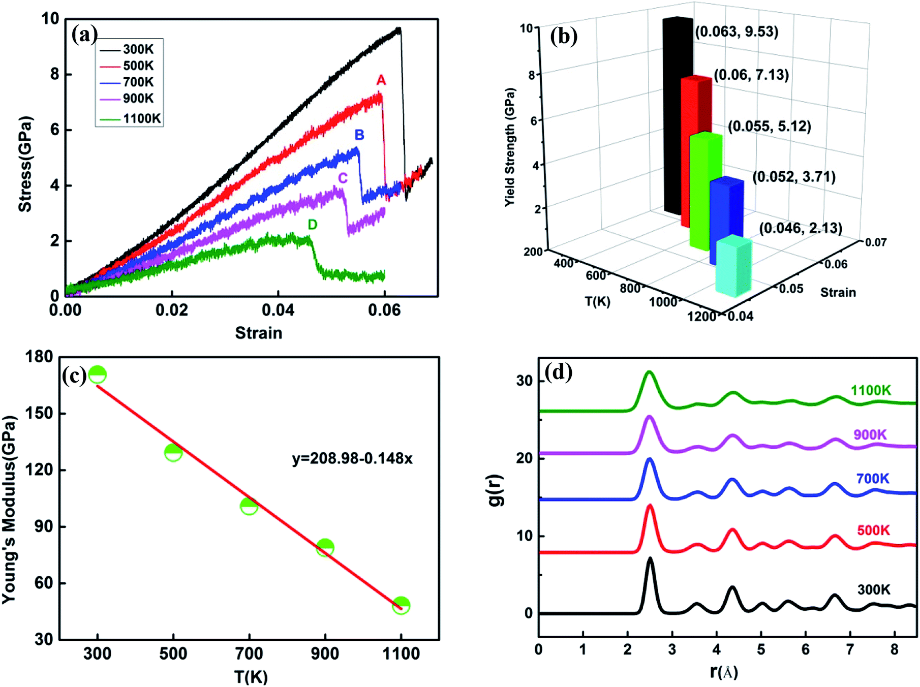 | ||
| Fig. 6 (a) Stress–strain curves of Ni–Co alloy nanowires. (b) Yield strength of alloy with different temperature. (c) Young's modulus of alloy. (d) Radial distribution function of Ni–Co alloy nanowires. | ||
For the purpose of further investigating the effect of temperature on the deformation mechanism, the snapshots at yield points (according to the A-D points in Fig. 6a) under different temperatures are used to analyze the distinction. Fig. 7a shows the state corresponding to the yield point of the nanowire at a temperature of 500 K. The color meanings shown in Fig. 7 are consistent with those described in Fig. 3. The number of disordered atoms in the system increases significantly, and the stacking fault caused by dislocation motion is found. When the temperature comes to 700 K, the structure state of the nanowire when yielding behavior occurs is shown in Fig. 7b. It is observed that the disordered atoms in the system continued to increase, and the generated stacking fault region became smaller, as illustrated by blue atoms. In Fig. 7c, the same change can be observed in the configuration state at 900 K temperature. The number of disordered atoms increases sharply, while the number of atoms with fcc structure decreases obviously. When the temperature rises to 1100 K, it can be seen from Fig. 7d that the system is dominated by disordered atoms, and the yield behavior is mainly affected by temperature, and no obvious stacking fault is observed. This is because that the thermal vibration between atoms intensifies when the temperature increases, making it different to observe the stacking fault, meanwhile, the factor affecting atom distribution and internal structure transmits from dislocation to temperature.
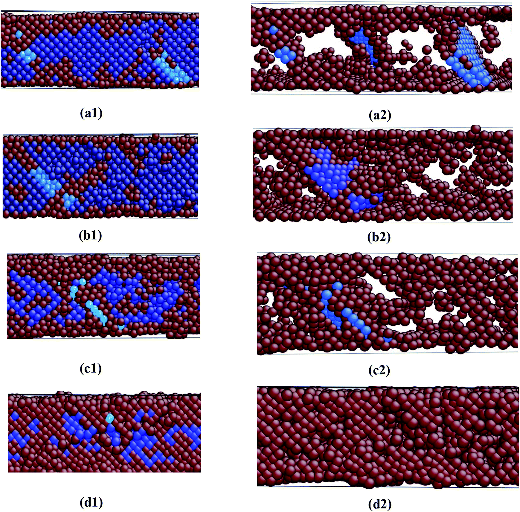 | ||
| Fig. 7 Snapshots of nanowire at yield points with different temperature under tensile loading: (a) 300 K; (b) 700 K; (c) 900 K; (d) 1100 K. | ||
Fig. 8 depicts the relationship between dislocation line length and strain in the nanowires under different temperatures. It is found that with the rise of temperature from 300 K to 1100 K, the dislocation line length in the system significantly decreases. When the temperature is 300 K, the dislocation line length shows the larger values at different strains and a highest value of 78 Å is obtained. When the temperature elevates to 1100 K, the dislocation line length exhibits the lower values. Meanwhile, with the increasing of temperature, the strains of the initial dislocation occurred decreases gradually (herein called as the strain advance phenomenon), which is corresponding to Fig. 6a.
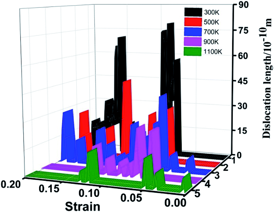 | ||
| Fig. 8 The relationship between dislocation line length and strain in alloy nanowires with different temperatures under tensile loading. | ||
As the temperature increases, the dislocation lines generated are shorter and easy to disappear due to the disorder of atomic structure. The formation of Hirth dislocation is consistent with that of stairs-rod dislocation, but partial dislocations have different reaction directions on the slip plane. The relationship between the strain and the length of different types of dislocation lines generated under different temperatures is illustrated in Fig. 9. Frank, Hirth, stair-rod and Shockley dislocations are present in the loading. Firstly, it is observed that the length of all kinds of dislocation lines decreases obviously with the increase of temperature. From Fig. 9a, it can be found that stair-rod and Shockley dislocations are dominated in the nanowires. When the temperature rises to 500 K, the stair-rod dislocation disappears and a small amount of Frank dislocations form in Fig. 9b. In the case of 700 K in Fig. 9c, a little of emerging Hirth dislocations generate with the length of 10 Å. There are no Frank and stair-rod dislocations at this time. When the temperature are in the range of 900–1100 K in Fig. 9d and e, the stair-rod and Shockley dislocations are still main role in the nanowires, similar to that at 300 K. However, the length values of the two kinds of dislocations decrease obviously. In brief, the increase of temperature within a certain range can promote the generation of Frank dislocation and Hirth dislocation, and with the further increasing of temperature the two types of dislocations disappear.
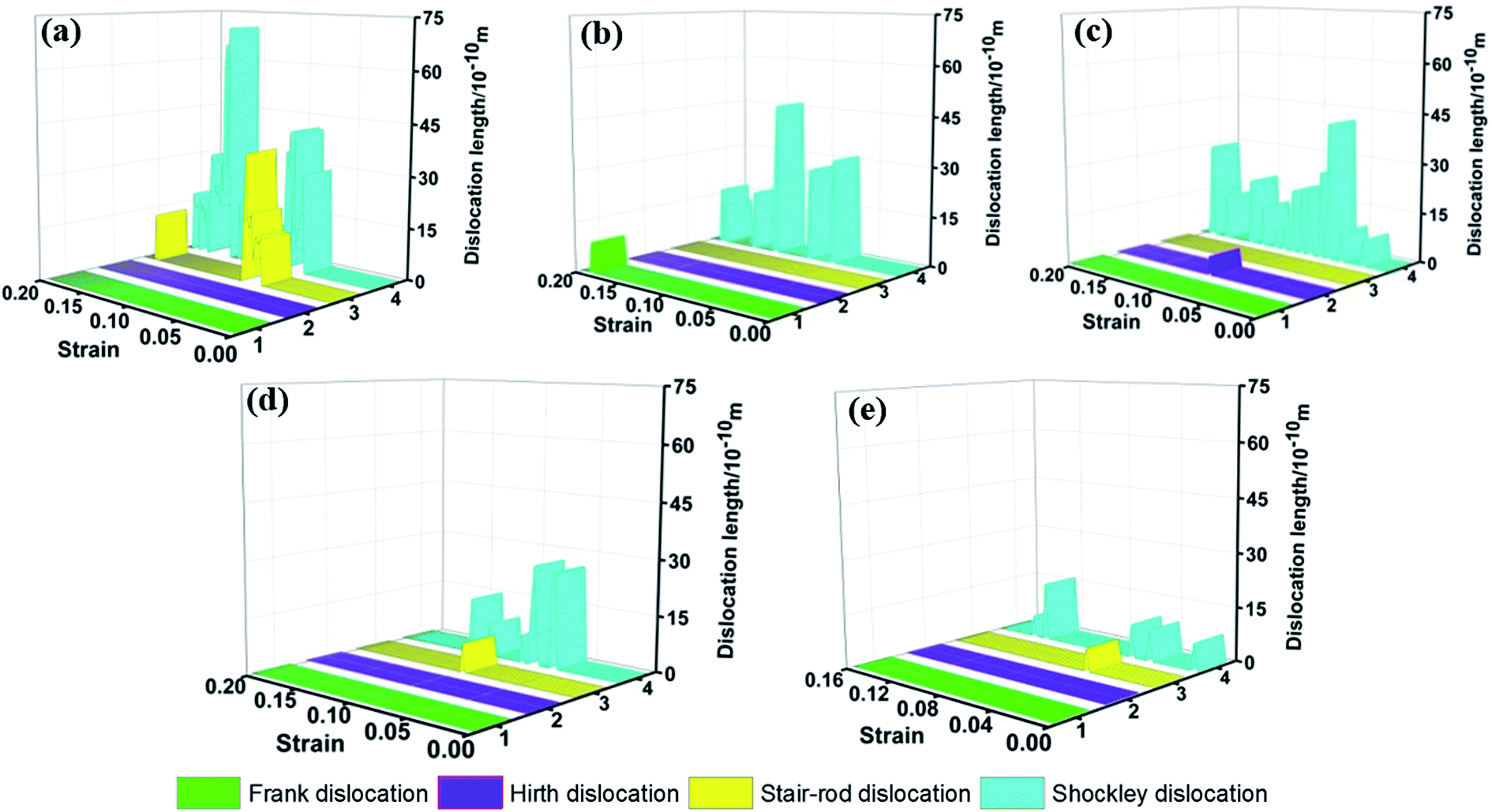 | ||
| Fig. 9 The dislocation types and length changes of alloy nanowires at different temperatures during loading: (a) 300 K; (b) 500 K; (c) 700 K; (d) 900 K; (e) 1100 K. | ||
Effect of void defect on tensile mechanical performance of Ni–Co alloy nanowire
In practical applications, it is still difficult to produce nanowires with perfect structure. Defects are often found and mainly include large voids, vacancies and gaps, which may appear on the surface and at the core. Sheikh F. and others36 analysed the influence of defects on the mechanical performance and found that the existence of defects and has a larger effect on the performance. The crack growth of nickel base single crystal alloy under shear loading was studied by molecular dynamics, and it was analyzed that the presence of preset defects could accelerate dislocation nucleation and crack growth, thus reducing the performance of the alloys to a certain extent.37 Brochard et al.38 through studying the mechanism of internal defects in the FCC nanowires, the discovery of internal defects is considerable assist to the nucleation of dislocation and the failure of nanowires. Heino P. et al.39 studied the fracture of copper nanowires with different defect types, and observed that as the source of cracks, defects can reduce the strain strength of nanowires until they break. Therefore, it is particularly important to understand the mechanism of the influence of the existence and location of defects on the material properties.In this part of the work, the influence of defect location factors on the properties of nanowires was investigated. The built defect models of system are shown in Fig. 11a and 12a, which are obtained through removing about 0.3% of the atoms (41 atoms) in the surface and internal of the nanowires as the introduction of void defects. The effects of void defects on the performance of alloy nanowires are studied by contrasting the deformation behaviors of the perfect, surface void and internal void. Fig. 10a is the stress–strain curve of the tensile process of the alloy nanowires with and without defects. It can be clearly seen that the introduction of defects has a great influence on the properties of nanowires. After the introduction of the inner void, the yield strength of the nanowire drops to 6.6 Gpa, and the yield strength of the surface void decreases by a relatively small extent, which can be observed in Fig. 10a and b. The yield strains of the nanowire drop to 0.043 and 0.056, respectively, lower than that of perfect nanowire of 0.063. Fig. 10c shows that potential energy of the nanowire increases with the change of strain, and the potential energy of the internal defect is slightly higher than that of the surface defect. When the yield behavior occurs, the dislocation movement and stacking fault are present in the nanowire, resulting in a process of energy decline, which is similar to the evolution process after the yield point in Fig. 10a.
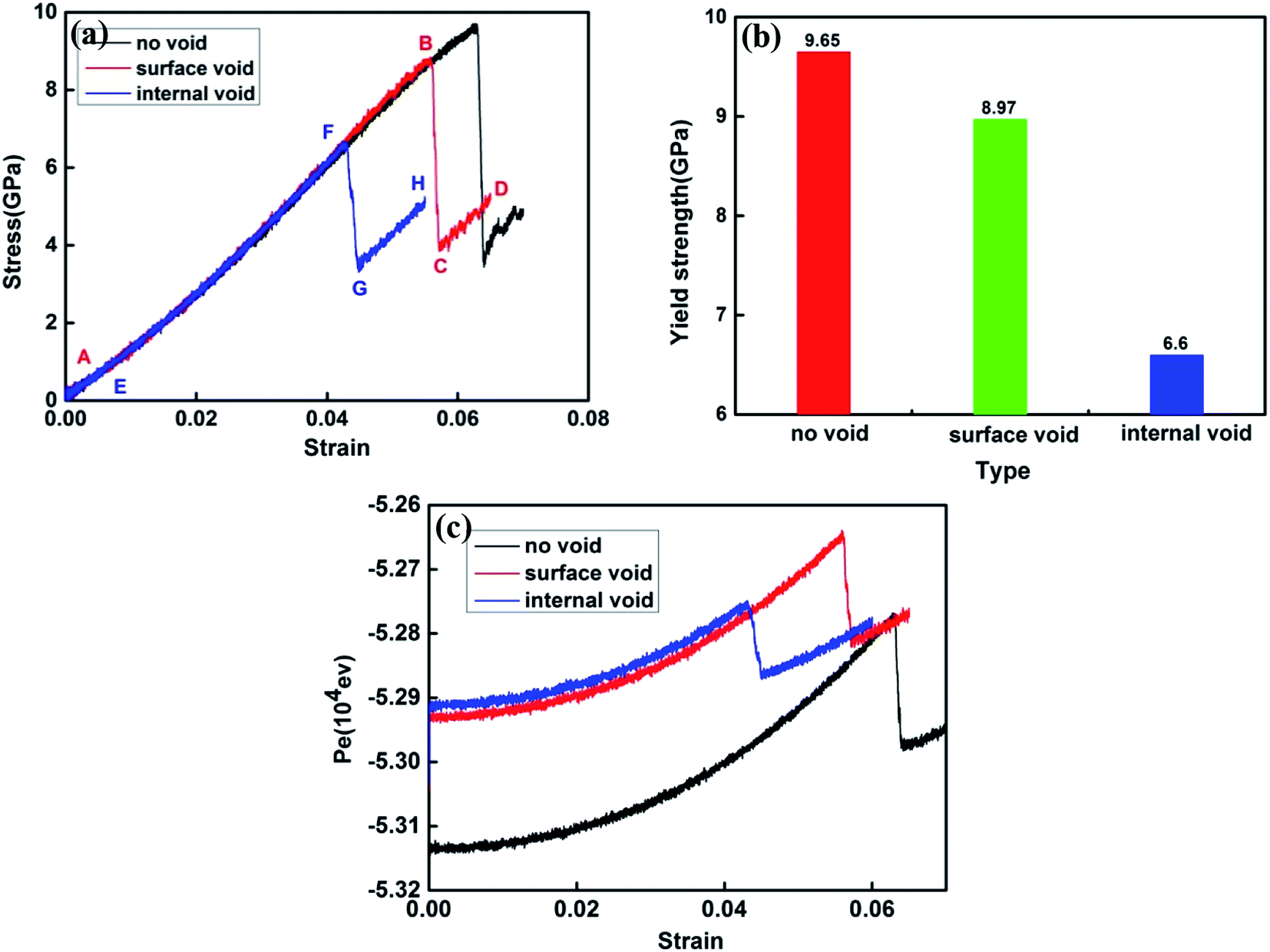 | ||
| Fig. 10 (a) Stress–strain curves of Ni–Co alloy nanowires. (b) Yield strength of alloy with different void defects. (c) Potential energies of Ni–Co alloy nanowires. | ||
In the middle part of the nanowire, atoms in the rectangular frame with the size of 1 × 1 × 4 Å3 are removed to form the surface void. The color meanings shown in Fig. 11 and 12 are consistent with those described in Fig. 3. Fig. 11a is the initial state of the nanowire with surface void. Fig. 11b is the state corresponding to the yield of nanowires with surface void when ε = 0.0558 (yield strain). The cyan atomic structure represents a stacking fault, and the pink line represents a dislocation. It can be seen that the dislocation first formed at the end of the void and caused the generation of stacking fault, as demonstrated by a few blue atoms. When ε = 0.0572, Fig. 11c is the dislocation formed at the end of the surface void continues to expand after the yield behavior occurring, and the area of the stacking fault increases correspondingly. In Fig. 11d, when ε = 0.065, tiny steps (as shown by orange circle line) are left when the dislocation line extends to the surface of the nanowire, and the stacking fault also spreads through the upper and lower surface of the nanowire (as shown by orange arrows).
 | ||
| Fig. 11 Snapshots of the deformation behavior of the nanowires with surface void in the process of tensile loading with different strains: (a) 0; (b) 0.0558; (c) 0.0572; (d) 0.065. | ||
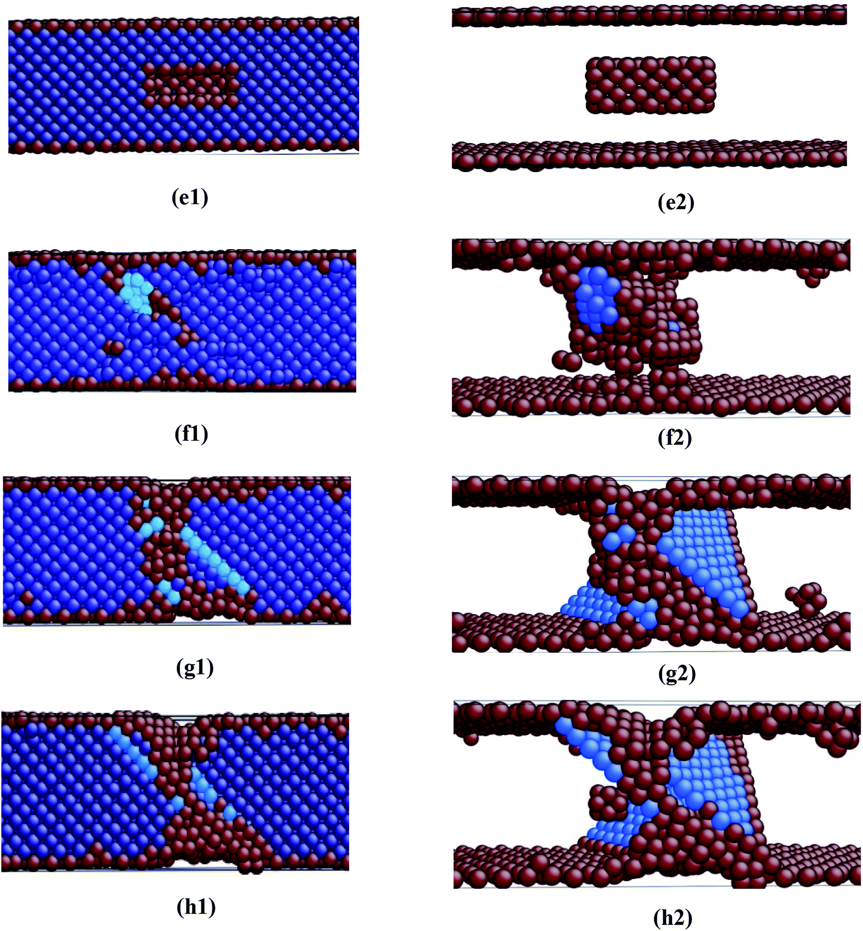 | ||
| Fig. 12 Snapshots of the deformation behavior of the nanowires with internal void in the process of tensile loading with different strains: (e) 0; (f) 0.043; (g) 0.045; (h) 0.0548. | ||
Similarly, the atoms in the rectangular frame with the size of 1 × 1 × 4 Å3 are removed in the middle of the nanowires to form internal void, as shown in Fig. 12e, which is the initial structure state of the alloy nanowires with internal void. Fig. 12f shows the state of yield behavior of nanowire at ε = 0.043. It can be seen that the disordered atoms are gather around the inner void, and the initial dislocations and stacking fault (blue atoms) can be observed. When ε = 0.045, it is found that the expansion of dislocation leads to the formation of stacking fault, as described in Fig. 12g. Meanwhile the necking phenomenon of nanowire occurs. When the strain increases to 0.0548, it is shown in Fig. 12h that the accumulation of stacking fault and the aggravation of necking phenomenon can be observed. To sum up, the initial dislocation sources both occur around the void defects. Also, the location of defects has a great impact on the mechanical properties of nanowires. The nanowire with internal void defect has lower yield strength and yield strain, and shows the whole higher potential energies in the tensile process.
Fig. 13 describes the relationship between dislocation line length and strain in the nanowires in three cases. For the presence of internal void defect, the dislocation line length first increases and then decreases gradually when the strain is above 0.13, and the total dislocation line length is the longest in three cases. In addition, the length of dislocation line is shorter at the initial dislocation formation phase and increases dramatically when the strain exceeds 0.17.
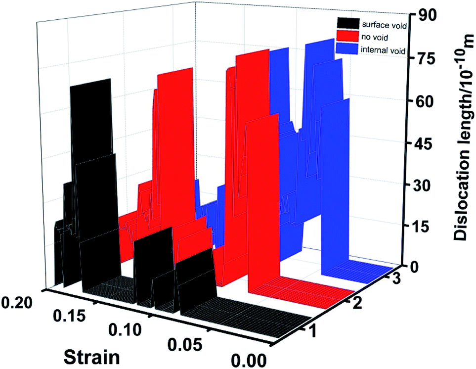 | ||
| Fig. 13 The relationship between dislocation line length and strain in alloy nanowires with different void defect under tensile loading. | ||
Corresponding to Fig. 11, the nanowires with surface voids generate partial dislocations from stress concentration at the voids and expand with loading. There is no mutual reaction between dislocations, so no other dislocations are generated. Corresponding to Fig. 12, the deformation of nanowires with internal voids is relatively complex, and the interaction between partial dislocations promotes the formation of new dislocations. Shockley dislocation combines to generate perfect dislocation, reducing stress concentration and promoting dislocation movement on the slip plane. Fig. 14 shows the relationship between the strain and the length of different types of dislocation lines generated under different defect types. It is found that only Shockley dislocation exists in the structure for surface defect in Fig. 14b, and the length of initial nucleation dislocation is relatively short with the value of 10 Å. Fig. 14c illustrates the perfect, Hirth, stair-rod and Shockley dislocations are all formed in the nanowires. Compared to Fig. 14a, the Shockley dislocation line length decreases to 56 Å while the stair-rod dislocation line length increases to 46 Å, meanwhile, the length of the initial nucleating dislocation is comparatively long. Subsequently, the early formation stage of perfect and Hirth dislocations locate at the strain of about 0.062. With the process of loading, the Hirth dislocation is invisible and the two slight peaks can be observed for perfect dislocation at strain of 0.15.
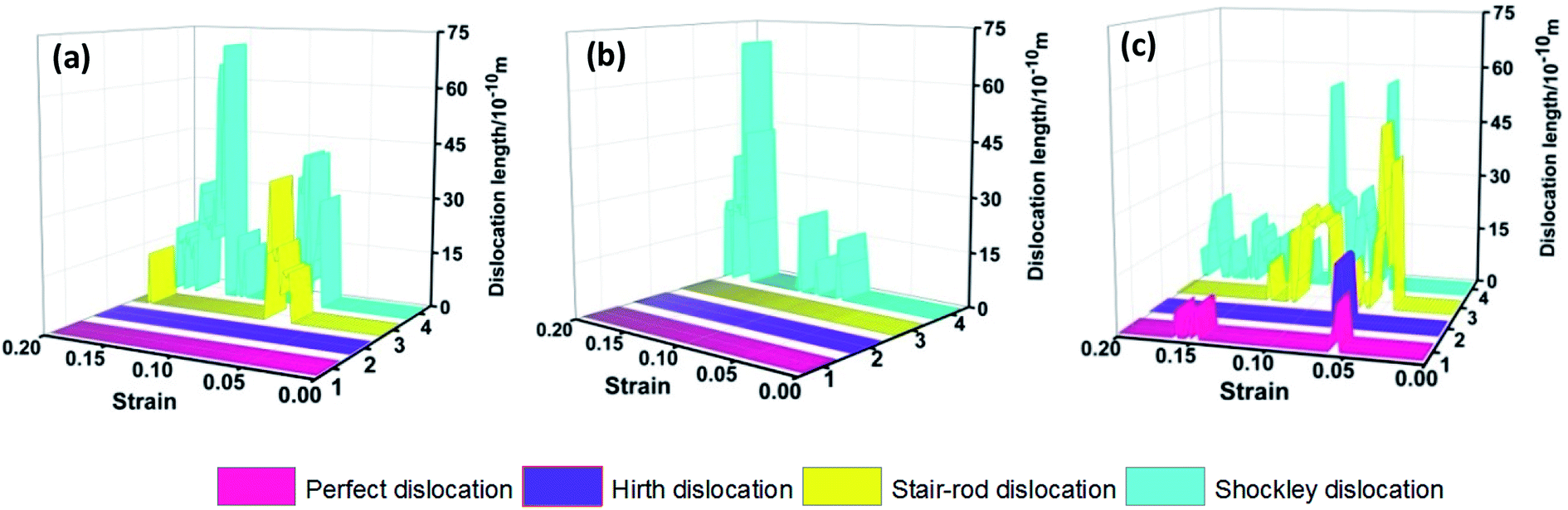 | ||
| Fig. 14 The dislocation types and length of the defective nanowires vary with strain during loading. (a) Perfect nanowire; (b) surface defect nanowire; and (c) internal defect nanowire. | ||
Conclusions
In this paper, the effects of Co content, temperature and void defects on the tensile mechanical properties of Ni–Co alloy nanowires were studied by molecular dynamics simulation.The results showed that:
Under the tensile loading, the increase of Co content can improve the mechanical properties of nanowires to a certain extent. The yield strength of nanowire with 5% and 10% Co content is higher. Moreover, Frank dislocation in alloy nanowires with 5% Co content and stair-rod dislocation in nanowire with 10% Co content greatly contribute to the improvement of nanowires performance.
When the temperature is in the range of 300 K to 1100 K, the yield strength of the nanowire goes down from 9.53 to 2.13 GPa. Specially, when the temperature is 500 K, the formation of Frank dislocation becomes easier. As the temperature is 700 K, the Hirth dislocation with length of 8 Å is formed in the nanowires.
The influence of surface and internal void on alloy nanowires is mainly reflected in the fact that the defect is used as the dislocation source to emit dislocation, resulting in easier formation of dislocation and lower yield point of nanowires. The yield strength of nanowire with internal void decreases about 30%, lower than that of nanowire with the perfect nanowire. When internal void defect exists in nanowire structure, it is easy to form perfect dislocation and Hirth dislocation. With the presence of surface void defect, only Shockley dislocations occur in the nanowires.
Conflicts of interest
There are no conflicts to declare.Acknowledgements
The work was supported by the National Key R&D Program of China (Grant No. 2017YFA0700701, 2017YFA0700703), the National Natural Science Foundation of China (Grant No. 51662026), and the Joint Fund between Shenyang National Laboratory for Materials Science and State Key Laboratory of Advanced Processing and Recycling of Nonferrous Metals (Grant No. 18LHPY001).Notes and references
- Y. Liu, H. Yang, Y. Liu, B. Jiang and R. Woodward, Acta Mater., 2005, 53, 3625 CrossRef CAS.
- R. Nishida, P. Puengjinda and H. Nishino, RSC Adv., 2014, 4, 16260 RSC.
- C. L. Yang, Z. J. Zhang, P. Zhang, C. Y. Cui and Z. F. Zhang, Mater. Sci. Eng., A, 2018, 736, 100 CrossRef CAS.
- B. Habibi and N. Delnavaz, RSC Adv., 2016, 6, 31797 RSC.
- L. Wang, Y. Gao, Q. Xue, H. Liu and T. Xu, Appl. Surf. Sci., 2005, 242, 326 CrossRef CAS.
- M. M. Kamel, J. Appl. Electrochem., 2007, 37, 483 CrossRef CAS.
- B. Y. C. Wu, C. A. Schuh and P. J. Ferreira, Metall. Mater. Trans. A, 2005, 36, 1927 CrossRef.
- A. Ghahremaninezhad and A. Dolati, J. Alloys Compd., 2009, 480, 275 CrossRef CAS.
- A. S. Samardak, A. V. Ognev and A. Y. Samardak, J. Alloys Compd., 2018, 732, 683 CrossRef CAS.
- M. J. Hu, B. Lin and S. H. Yu, Nano Res., 2008, 1, 303 CrossRef CAS.
- V. Solanki, O. I. Lebedev, M. Motin Seikh, N. K. Mahato, B. Raveau and A. K. Kundu, J. Magn. Magn. Mater., 2016, 420, 39 CrossRef CAS.
- Y. H. You, C. D. Gu, X. L. Wang and J. P. Tu, Surf. Coat. Technol., 2012, 206, 3632 CrossRef CAS.
- K. Maaz, J. L. Duan, S. Karim, Y. H. Chen, H. J. Yao, D. Mo, Y. M. Sun and J. Liu, J. Alloys Compd., 2016, 662, 296 CrossRef CAS.
- H. Akbarzadeh, E. Mehrjouei, S. Ramezanzadeh and C. Izanloo, J. Mol. Liq., 2017, 248, 1078 CrossRef CAS.
- N. C. Lindquist, P. Nagpal and K. M. Mcpeak, Rep. Prog. Phys., 2012, 75, 36501–36510 CrossRef PubMed.
- J. Zhou, R. S. Averback and P. Bellon, Acta Mater., 2014, 73, 116 CrossRef CAS.
- D. S. Hecht, L. Hu and G. Irvin, Adv. Mater., 2011, 23, 1482 CrossRef CAS PubMed.
- L. Y. Qin, J. S. Lian and E. C. Jiang, Chin. J. of Nonferrous Met., 2013, 23, 2846 CAS.
- C. L. Yang, Z. J. Zhang and P. Zhang, Mater. Sci. Eng., A, 2018, 736, 100 CrossRef CAS.
- L. Qin, J. Lian and Q. Jiang, J. Alloys Compd., 2010, 504, S439 CrossRef.
- S. Mojumder, Phys. B, 2018, 530, 86 CrossRef CAS.
- S. Plimpton, J. Comput. Phys., 1995, 117, 1 CrossRef CAS.
- G. P. Purja Pun, V. I. Yamakov and Y. Mishin, Modell. Simul. Mater. Sci. Eng., 2015, 23, 065006 CrossRef.
- Y. Zhang, K. Jin and H. Xue, J. Mater. Res., 2016, 31, 2363 CrossRef CAS.
- M. S. Daw, S. M. Foiles and M. I. Baskes, Mater. Sci. Rep., 1993, 9, 251 CrossRef CAS.
- G. P. Purja Pun and Y. Mishin, Phys. Rev. B: Condens. Matter Mater. Phys., 2012, 86, 134116 CrossRef.
- Y. Mishin, Acta Mater., 2004, 52, 1451 CrossRef CAS.
- J. Li, Mater. Sci. Eng., 2003, 11, 173 Search PubMed.
- A. Stukowski, Modell. Simul. Mater. Sci. Eng., 2010, 18, 015012 CrossRef.
- J. D. Honeycutt and H. C. Andersen, J. Phys. Chem., 1987, 91, 4950 CrossRef CAS.
- D. Faken and H. Jónsson, Comput. Mater. Sci., 1994, 2, 279 CrossRef CAS.
- A. Stukowski, V. V. Bulatov and A. Arsenlis, Modell. Simul. Mater. Sci. Eng., 2012, 20, 085007 CrossRef.
- G. Lu and G. Shen, Phys. Status Solidi, 2010, 63, 705 Search PubMed.
- Z. Cheng, H. Zhou, Q. Lu, H. Gao and L. Lu, Science, 2018, 362, 1 Search PubMed.
- W. C. Xu, P. Q. Dai and Y. D. Zheng, Chin. J. of Nonferrous Met., 2010, 20, 92 CrossRef CAS.
- S. F. Ferdous and A. Adnan, Comput. Mater. Sci., 2014, 90, 221 CrossRef CAS.
- J. Yu, Q. Zhang and L. Rong, RSC Adv., 2014, 4, 32749 RSC.
- S. Brochard, P. Beauchamp and J. Grilhé, Mater. Res. Soc. Symp. Proc., 2001, 677, AA5.5.1 CrossRef.
- P. Heino, H. HäKkinen and K. Kaski, Phys. Rev. B: Condens. Matter Mater. Phys., 1998, 58, 641 CrossRef CAS.
| This journal is © The Royal Society of Chemistry 2019 |