
 Open Access Article
 This Open Access Article is licensed under a Creative Commons Attribution-Non Commercial 3.0 Unported Licence
Chemical exfoliation efficacy of semiconducting WS2 and its use in an additively manufactured heterostructure graphene–WS2–graphene photodiode
Jay A. Desaiabc,
Nirmal Adhikarid and
Anupama B. Kaul *bc
*bc
aDepartment of Metallurgical, Materials and Biomedical Engineering, University of Texas at El Paso, El Paso, TX 79968, USA. E-mail: anupama.kaul@unt.edu
bDepartment of Material Science and Engineering, Denton, TX 76203, USA
cPACCAR Technology Institute, Department of Electrical Engineering, University of North Texas, Denton, TX 76203, USA
dDepartment of Electrical Engineering, University of Texas at El Paso, El Paso, TX 79968, USA
First published on 16th August 2019
Abstract
In the present work, various chemical exfoliation routes for semiconducting two-dimensional (2D) layered material WS2 are explored, which include magnetic stirring (MS), shear mixing (SM), and horn-tip (HT) sonication. Current–voltage measurements, Raman spectroscopy, and photoluminescence (PL) spectroscopy were used to characterize the drop-casted WS2 nanosheets produced by these three techniques and our analysis revealed that HT sonication produced the most optimal dispersions. Heterostructure photodetector devices were then fabricated using inkjet printing of the HT sonicated dispersions of WS2 and graphene. The photodetector device performance was measured using a stream of ON/OFF light pulses generated using a red laser with wavelength λ ∼ 660 nm, and an arbitrary waveform generator. From this analysis, the photoresponsivity and detectivity of the graphene–WS2–graphene heterostructure devices were calculated to be ∼0.86 A W−1 and ∼1013 Jones, respectively. Capacitance–voltage (C–V) and C–frequency (f) measurements were also conducted, where the V was swept from –6 V to +6 V, while the change in C was measured from f ∼ 20 kHz up to 3 MHz to gain insights into the nature of the graphene–WS2 interface. From the C–V measurements, the C plateaued at ∼324.3 pF from ∼−4 V to +4 V for the lowest f of 20 kHz and it reduced to ∼200 pF from −6 V to ∼−4 V, and similarly from ∼4 V to 6 V, C was ∼190 pF. The decrease in C for V > +4 V and V < −4 V was attributed to the reduction of the interfacial barrier at the electrodes which is suggestive of a Schottky-based photodiode at the graphene–WS2 interface. A sharp decrease in C from ∼315.75 pF at 25.76 kHz to ∼23.79 pF at 480 kHz (at 0 V bias) from the C–f measurements suggests a strong effect of interface trap density on C built-up at the graphene–WS2 interface and the ensuing Schottky barrier height. Our work confirms the excellent potential of solution-cast, trilayer graphene–WS2–graphene heterostructures as a promising photodetector platform using additively manufactured inkjet printing.
1. Introduction
Since the first isolation of graphene in 2004,1,2 various layered materials have been the subject of extensive research, specifically, the transition metal dichalcogenides (TMDCs) that have shown great interest amongst researchers due to their interesting electronic,3 optical,4 mechanical,5 and chemical6 properties. They represent a class of materials with the formula MX2, where M is a transition metal element (e.g. Mo, W, Ti, V, or Nb) and X is a chalcogen (S, Se or Te). The TMDCs have a layered structure in the form of X–M–X, where two planes of chalcogen atoms are separated by a plane of the metal atoms.5 In many of these semiconducting TMDCs, such as MoS2 and WS2, an indirect-to-direct band gap transition is also observed when the bulk layered material is exfoliated to its monolayer form.7,8 These TMDCs also possess sizeable band gaps of ∼1 to 2 eV which positions them well for many electronic and optoelectronic devices and makes them attractive as viable alternatives to Si-based (bandgap ∼ 1.14 eV) or GaAs-based (bandgap ∼ 1.43 eV) electronics and optoelectronics.9While significant work has been conducted on the exfoliation studies of MoS2 to better understand its optical and electronic properties,10–14 the body of work on similar exfoliation studies on WS2 is sparser. In its bulk state, WS2 has an indirect bandgap of ∼1.4 eV but it morphs to a direct bandgap of ∼2.1 eV when thinned to its monolayer form,15 which makes it attractive for high-performance optoelectronics16–19 and photodetectors operational in the visible regime. Photodetectors are used in a wide range of applications from imaging to optical communication, as they convert light into electrical signals.20–24 Conventional semiconductors such as Si and GaAs used in photodetectors are usually opaque and their brittle nature limits their use on rigid substrates only. The band gap in the visible part of the electromagnetic spectrum and the presence of Van Hove singularities in the electronic density of states enables WS2 nanosheets to exhibit transparency while displaying strong light–matter interactions. They have also demonstrated high performance on flexible substrates with bending curvature down to 5 mm.25 These remarkable properties empower WS2 to overcome some of the limitations associated with conventional semiconducting channel materials (e.g. Si, GaAs) and promotes its use in bendable and transparent photodetector devices.26–28
The exfoliated WS2 nanosheets for photodetection and other applications involving the use of a semiconducting channel are produced using bottom-up approaches comprising of physical vapor deposition (PVD)29 or chemical vapor deposition (CVD),30 where the WS2 molecules assemble to form mesoscopic 2D nanosheets. The WS2 nanosheets may also be produced using a top-down approach such as mechanical31 or chemical exfoliation32 where layers of WS2 membranes are isolated from the bulk toward nanoscale dimensions. Moreover, liquid-phase or chemical exfoliation has been the subject of numerous studies, as it offers a range of advantages over other methods, which includes low-cost, low-temperature (as low as room temperature) processing, attractive scalability towards large formats and its material conserving nature.33,34 In general, oxidation and subsequent dispersion in appropriate solvents, ion-intercalation, ion-exchange, and sonication-assisted exfoliation remain commonly explored methods for chemical exfoliation.35 However, to date, there is no prior work that reports on comparing the efficacy of WS2 chemical exfoliation routes operational at near room temperature.
In the present work, we have conducted an extensive analysis of several exfoliation routes for forming eco-friendly dispersions of WS2, which includes magnetic stirring (MS), shear mixing (SM), and horn-tip (HT) sonication. After determining the optimal exfoliation route, graphene–WS2–graphene heterostructure photodetectors were designed and fabricated, where WS2 is used as the semiconducting channel material, and graphene, given its finite density of states at the k-point from Dirac cones of valence and conduction bands, chemical inertness, and high stability, is used as a highly conducting electrode material.36 Inkjet printing has been employed as a material-conserving technique for the precise deposition of graphene and WS2 nanosheets37,38 in picoliter volumes, which enables ink flow (printable liquid) from the cartridge to the substrate. The liquid undergoes some drying after impact on the substrate depending on the platen temperature used. Raman and photoluminescence (PL) spectroscopy, photocurrent Ip, capacitance–voltage (C–V), and C–frequency (f) measurements were amongst the techniques used to characterize our all inkjet-printed photodetector devices which are presented in this paper.
2. Results
As noted, the three techniques used in this work to disperse WS2 in chemical dispersions are magnetic stirring (MS), shear mixing (SM) and horn-tip (HT) sonication. These techniques are illustrated schematically in Fig. 1, which shows the various mechanisms and parameters used in producing single-to-few layer WS2 nanosheets. The first technique, MS, uses a magnetic field to create fluidic shear forces that are generated as a bar magnet is spun in the liquid to generate the stirring and exfoliation action illustrated in Fig. 1(a). The magnetic stirrer moves the fluid in a clockwise direction at predefined revolutions per minute (rpm). When a vial containing the magnetic stirrer and the liquid are placed above the hot plate, the magnetic stirrer also starts to move in a clockwise direction at the same rpm. The energy provided by stirring breaks the 3D layered materials into 2D nanosheets. In the second technique, SM, exfoliation results when a shear force is produced such that one area/layer of the fluid travels with a different velocity relative to the adjacent area/layer. Fig. 1(b) demonstrates the mechanism of shear mixing used in the current work. High-speed rotation of the rotor blades in a clockwise direction results in the shearing of nanosheets that experience a velocity differential, causing the layers to peel apart. The third technique, exfoliation by HT sonication, exposes the layered material to ultrasonic waves in an appropriate solvent by inducing vibrations through a horn-tip; this is shown in Fig. 1(c). Ultrasonic waves generate cavitation bubbles that collapse into high energy jets, breaking up the layered crystallites to produce exfoliated nanosheets.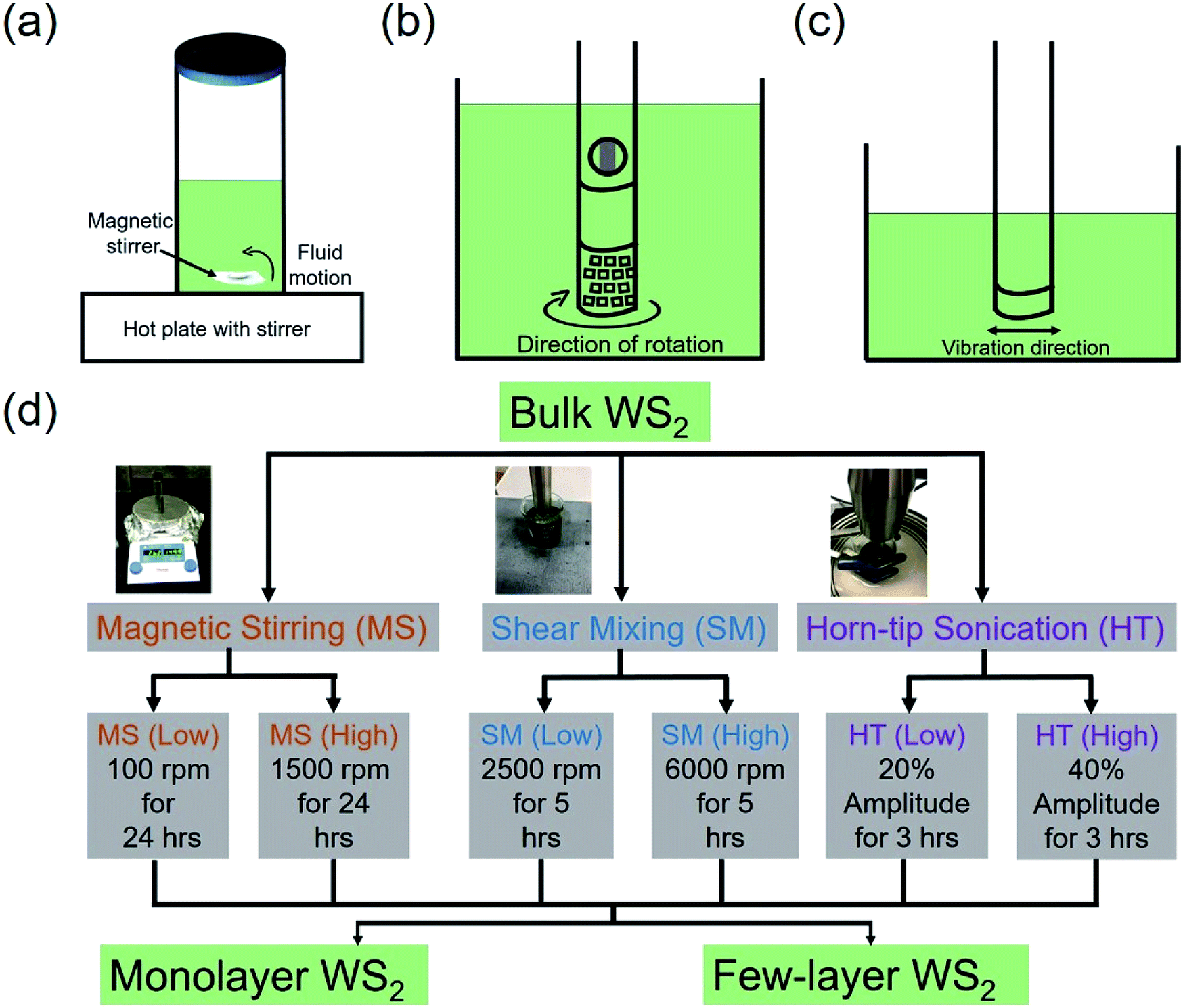 | ||
| Fig. 1 Mechanism of (a) magnetic stirring (MS), (b) shear mixing (SM), and (c) horn-tip sonication (HT). The MS exfoliation route utilizes a magnetic field to create fluidic shear forces that are generated as a bar magnet is spun in the liquid to exfoliate the material. The energy provided by stirring breaks the 3D layered materials into 2D nanosheets. The SM exfoliation route exploits the high-speed rotation of the rotor blades resulting in shearing nanosheets due to a velocity differential between them. The HT technique exposes the layered material to ultrasonic waves by inducing vibrations through a horn-tip. Ultrasonic waves generate cavitation bubbles that collapse into high energy jets, breaking up the layered crystallites to produce exfoliated nanosheets. (d) Schematic illustration of the various parameters used for the three techniques for WS2 ink preparation. The C/T/EC solution mixture of 5 ml, 50 ml, and 20 ml was used for MS, SM, and HT sonication, respectively. These were the minimum concentrations necessary to facilitate the exfoliation with each technique. | ||
The parameters used for MS, SM, and HT sonication are summarized in Fig. 1(d). Here, MS (low) and MS (high) refer to magnetic stirring conditions of 100 rpm and 1500 rpm for 24 hours, respectively. The SM at 2500 rpm and 6000 rpm for 5 hours is referred to as SM (low) and SM (high), respectively, whereas the HT sonication at 20% and 40% power amplitude is denoted as HT (low) and HT (high), respectively.
The I–V response for drop-casted, annealed MS (low) and MS (high) samples are depicted in Fig. 2(a), while the I–V characteristic for drop-casted, annealed SM (low) and SM (high) samples are shown in Fig. 2(b). The inset in Fig. 2(a) shows current data on an expanded scale for the MS (low) case. Similarly, Fig. 2(c) displays the I–V behavior for drop-casted and annealed HT (low) and HT (high) samples. All drop-casted samples demonstrated non-ohmic behavior, as shown in Fig. 2(a)–(c), suggestive of the strong semiconducting nature of the WS2 nanosheets. From the electronic transport data, it is evident that the higher electrical conductivity is obtained when WS2 is exfoliated at a higher speed of MS (Fig. 2(a)), higher speed of SM (Fig. 2(b)), and at a higher amplitude of HT sonication (Fig. 2(c)), when the time is kept fixed; this suggests that when the net power applied to the solution is greater, a higher exfoliation rate occurs in all of the three exfoliation routes examined.
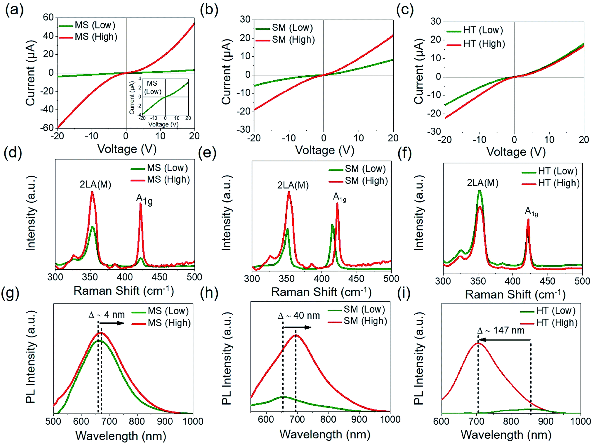 | ||
| Fig. 2 I–V measurements of drop-casted and annealed (a) MS (low) and MS (high) samples; inset shows the data for drop-casted and annealed MS (low) sample only on a magnified current scale. I–V Characteristic for (b) SM (low) and SM (high) samples, and (c) HT (low) and HT (high) samples. Magnetic stirring showed the highest value of electrical conductivity followed by HT sonication and SM but the dispersions generated using MS were unstable. Raman spectra of drop-casted and annealed (d) MS (low) and MS (high) samples, (e) SM (low) and SM (high) samples, (f) HT (low) and HT (high) samples. Intensity ratios [I2LA(M/IA1g] of MS (low) and MS (high) sample were found to be 3.83 and 1.17, respectively, indicating the presence of few-layer WS2. Intensity ratios of SM (low) and SM (high) samples were found to be 1.16 and 0.92, respectively, again indicating the presence of few-layer WS2. Intensity ratios of HT (low) and HT (high) samples were found to be 2.11 and 1.23, respectively, again indicating the presence of few-layer WS2. The intensity ratio values are summarized in Table 1. Photoluminescence spectra of (g) MS (low) and MS (high) samples, (h) SM (low) and SM (high) samples, and (i) HT (low) and HT (high) samples. Horn-tip sonication showed the highest blue-shift in the PL peak location from low-to-high conditions, where Δ ∼ 147 nm was tabulated, while Δ for SM was ∼40 nm (red-shifted) and Δ for MS was ∼4 nm (red-shifted). | ||
Raman and photoluminescence (PL) spectroscopy were used to characterize the ensuing material generated at the low- and high-level conditions for all the three exfoliation routes. In Raman spectroscopy, the interaction of an incoming laser with the molecular vibrations of the material under examination causes the energy of the reflected photons to either increase or decrease. This shift in energy gives information about the unique vibrational modes that serve as fingerprints of the material.39–41 In WS2, there are two primary Raman active modes, the A1g mode which arises from the out-of-plane vibrations involving only sulfur atoms and occurs at ∼418.8 cm−1 and the 2LA(M) mode at ∼352.4 cm−1 due to the in-plane displacement of the tungsten and sulfur atoms. The number of layers may be estimated by either monitoring the red-shift in the A1g mode which refers to the lattice relaxation phenomenon due to the removal of layers,42 or by calculating the intensity ratio, I2LA(M)/IA1g.43 As the exfoliation efficacy improves, the number of layers should decrease as deduced from the intensity ratio calculation which is the technique we utilized here. When I2LA(M)/IA1g > 2.2 it is suggestive of monolayers, I2LA(M)/IA1g < 0.47 signifies WS2 in its bulk form, and 0.47 < I2LA(M)/IA1g < 2.2 occurs for few-layer WS2. Fig. 2(d) shows the Raman spectra of MS (low) and MS (high) samples. The I2LA(M)/IA1g [MS (low)] and I2LA(M)/IA1g [MS (high)] were calculated to be ∼3.83 and 1.17, respectively, indicating the presence of monolayer WS2 and few-layer WS2. Similarly, Fig. 2(e) displays the Raman spectra of SM (low) and SM (high) samples. The I2LA(M)/IA1g [SM (low)] and I2LA(M)/IA1g [SM (high)] samples were found to be ∼1.16 and 0.92, respectively, again indicating the presence of few-layer WS2. Finally, Fig. 2(f) shows the Raman spectra of HT (low) and HT (high) samples. The I2LA(M)/IA1g [HT (low)] and I2LA(M)/IA1g [HT (high)] were determined to be 2.11 and 1.23, respectively, again indicating the presence of few-layer WS2. The I2LA(M)/IA1g ratio of all the samples is summarized in Table 1.
| MS (low) | MS (high) | SM (low) | SM (high) | HT (low) | HT (high) | |
|---|---|---|---|---|---|---|
| I2LA(M)/IA1g | 3.83 | 1.17 | 1.16 | 0.92 | 2.11 | 1.23 |
Photoluminescence refers to the emission of light from a material after the absorption of photons. An extremely weak PL intensity is an indication of optical transitions that are poor and commonly associated with the indirect band-gap transitions in bulk 2D semiconducting samples.44 The intensity of the PL spectra increases with a reduction in the number of atomic layers, suggesting direct interband transitions, and reaches a maximum when monolayers are formed. Full-width-at-half-maximum (FWHM) and PL peak shift Δ, were calculated in order to study and compare PL behavior for the low- and high-conditions for each of the three exfoliation routes. Fig. 2(g) shows the PL spectra of the MS (low) and MS (high) samples, where a single peak is evident. However, the PL peak of the MS (high) sample is broader with FWHM ∼ 90.4 nm and is red-shifted with Δ ∼ 4 nm compared to the PL peak of the MS (low) sample which exhibited a FWHM ∼ 87.2 nm. Fig. 2(h) shows the PL spectra of the SM (low) and SM (high) samples displaying a single peak, but the FWHM was higher ∼144.4 nm for the SM (high) sample, and the red-shift Δ was ∼40 nm compared to the SM (low) sample with FWHM ∼ 43.6 nm. Fig. 2(i) shows the PL spectra of the HT (low) and HT (high) samples. The PL spectra of the HT (high) sample showed a strong single peak with FWHM ∼ 142.6 nm and Δ is blue-shifted significantly approaching ∼147 nm from the weakly defined PL peak of HT (low) sample. It's interesting to note that the HT sonicated samples were the only ones where the PL peak was blue-shifted at the higher conditions, while the MS and SM samples exhibited red-shifts in the PL peaks. The higher PL intensity of MS (high), SM (high), and HT (high) relative to the MS (low), SM (low), and HT (low), respectively, suggests a greater degree of exfoliation toward thinner molecular membranes.
The higher electrical conductivity of the MS (high), SM (high), and HT (high) samples may be due to the lower resistance offered by the few-layer WS2 nanosheets since inter-layer transport amongst the van der Waals solids is typically poor.45,46 However, MS (low) and MS (high) samples appeared to be unstable and WS2 nanosheets precipitated to the bottom of the vial in less than 12 hours. On the other hand, SM (low), SM (high), HT (low) and HT (high) samples were stable for at least 1 month, indicating the practical utility of such inks for prototype device platforms with ink jet printing. The images of the as-prepared solutions and after 12 hours of storage are shown in Fig. 3(a) and (b), respectively. These images illustrate the slightly greyer solution in (b) for the MS (high) case after 12 hours of storage compared to the starkly black dispersion in the as-prepared case in the left-most vial of Fig. 3(a), which suggests that precipitation is occurring after storage for the MS dispersions. In contrast, no visual precipitation or color changes were observed for the SM and HT samples implying their greater stability, to first order. However, HT (high) samples showed higher electrical conductivity among the four stable dispersions, and coupled with the fact that HT sonication resulted in a significant blue-shift of the PL peak, suggestive of quantum confinement effects arising from thinner membranes. It is interesting to note that sonication indeed reduces membrane size of our 2D semiconducting materials as based on our prior studies on WS2. Here the mean size for the as received WS2 powder was ∼18 μm which was reduced to above 2 μm after sonicating for 30 min. Interestingly, mean particle size for the first mode remained largely unchanged with sonication times of up to 18 hours.47 Additionally, the thickness of the printed patterns/films can be controlled with the number of printing passes. As an example, we have reported the change in thickness of graphene patterns that were formed using similar procedures, where the thickness changed from ∼505 nm for 10 printing passes to ∼1667 nm for 50 printing passes in our recent prior work.48 Given that HT sonication resulted in thinner membranes based on the Raman and PL data, it was used as the approach of choice for inkjet printing our photodetector devices which we report on next.
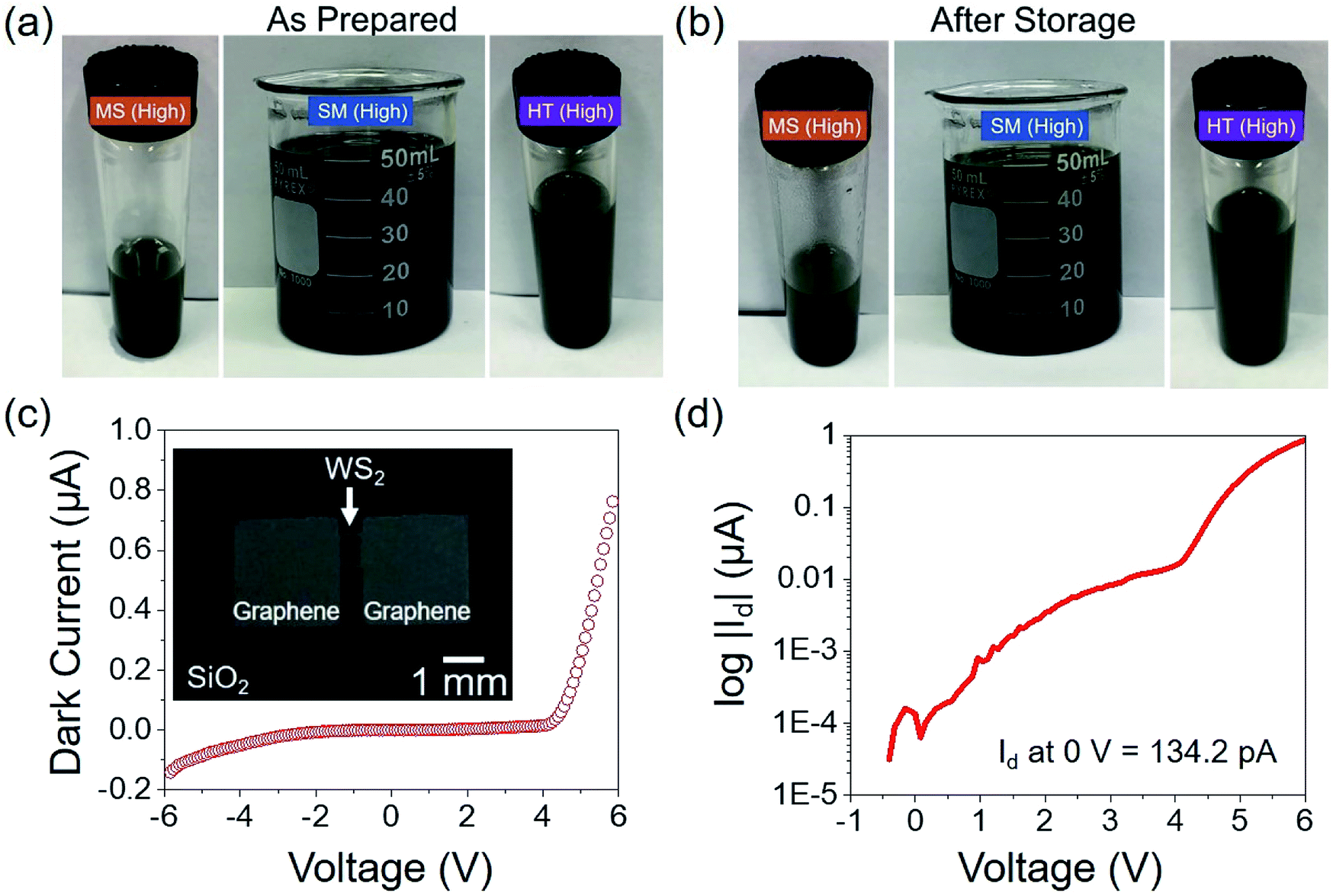 | ||
| Fig. 3 Optical images of MS (high)-left, SM (high)-middle, and HT (high)-right samples for (a) as prepared, and (b) after 12 hours of storage. The MS (high) sample showed precipitation of WS2 nanosheets after 12 hours due to the greyer solution dispersion in (b)-left, whereas the SM (high)-middle and HT (high)-right samples showed no visible precipitation given the darker colored dispersions persistent after storage. (c) The dark current Id–V measurement of inkjet printed graphene–WS2–graphene heterostructure device where the inset depicts the inkjet printed graphene–WS2–graphene heterostructure sample. (d) Dark current Id–V measurement on a log-scale which shows that Id ∼ 134.2 pA at 0 V which was the value used for the responsivity and detectivity calculations. | ||
Horn-tip sonication was used at a 40% power amplitude for 3 hours to form the graphene and WS2 inks. The line pattern of 1 mm (width) and 0.8 mm (length) were printed using the WS2 inks at 40 passes followed by annealing at 250 °C for 2 hours. Two 3 mm × 3 mm graphene pads were then printed overlapping regions of the WS2 at the edges, such that the effective WS2 channel length was 0.6 mm, and the samples were then again annealed at 250 °C for 2 hours. The inset in Fig. 3(c) shows a representative image of the inkjet printed graphene–WS2–graphene trilayer heterostructure device. Fig. 3(c) illustrates the dark current Id–V characteristic. The same Id–V graph is also plotted on a log scale, as depicted in Fig. 3(d), where Id was measured to be ∼134.2 pA at 0 V; this value is used in our subsequent calculations for determining the device's electrical response to incident light or responsivity R, and the photodetector's sensitivity to incident light or detectivity D. The non-ohmic variation of dark current with voltage is an indication of the rectifying metal–semiconductor junction formation at the graphene–WS2 interface, akin to a Schottky diode.
We then proceeded to make photodetector device measurements for which the measurement set up is displayed in Fig. 4(a), where an Agilent 33220A 20 MHz arbitrary waveform generator is used as the source of pulses to drive a ThorLabs laser source to produce a stream of periodic ON/OFF light pulses. The ThorLabs S1FC660 laser light source is used which lases at a wavelength λ ∼ 660 nm through the process of optical amplification. The laser light irradiates the device under test (DUT) mounted inside the Lakeshore CRX-4K cryogenic vacuum probe station. When the laser interacts with the semiconducting WS2 channel, enhanced electrical conductivity is obtained due to additional charge carriers generated by photon absorption. Laser ON and OFF cycles were generated and the current–time response of the device was captured using the Keysight B1500A semiconductor device analyzer, equipped with the medium power SMU B1511B module. The laser power Plaser, was varied by changing the input voltage from 1 V to 5 V in the waveform generator, referred to as Vwg which enabled Plaser to vary from 2.29 mW cm−2 to 12.13 mW cm−2. A linear relation was observed between Plaser and the Vwg which is reproduced in Fig. 4(b). Fig. 4(c) illustrates the time-dependent photoresponse of the inkjet printed graphene–WS2–graphene heterostructure device, where the photocurrent Ip increases with Plaser, as Plaser rose from 2.29 mW cm−2 to 12.13 mW cm−2.
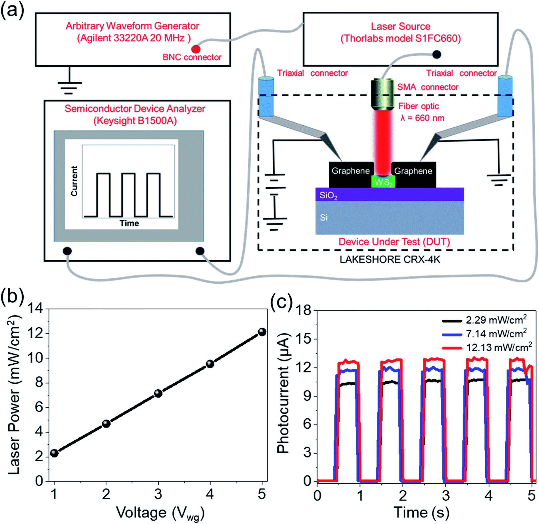 | ||
| Fig. 4 (a) Photodetection measurement set-up comprising of an arbitrary waveform generator as a source of pulses to provide input to the laser source, which lases at λ ∼ 660 nm and was used to irradiate the DUT placed in the probe station. The semiconductor device analyzer is used to measure the photocurrent output. (b) Variation of laser power Plaser with the input voltage Vwg. The magnitude of the Plaser is altered by changing the Vwg. Higher Vwg leads to higher Plaser generation. (c) Variation in photoresponse of the inkjet printed graphene–WS2–graphene heterostructure device for three levels of Plaser used. The Plaser is directly proportional to photocurrent generation, where the higher Plaser generates a larger number of charge carriers which leads to a higher photocurrent. | ||
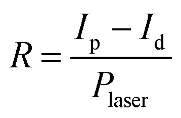
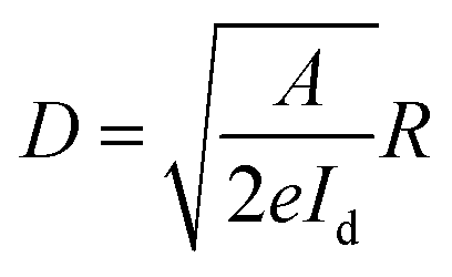
The magnitude of Ip, τr, τd, ON/OFF ratio, R, and D are key figures-of-merit for characterizing the performance of photodetectors. The time required by the photodetector to reach 90% of maximum Ip value when the laser is switched ON is referred as the rise time and is denoted by τr, whereas the time required by the photodetector to reach 10% of the maximum Ip value when the laser is switched off from it's ON state is referred to as decay time and is denoted by τd,. The ON/OFF ratio refers to the ratio of the ON-state current and OFF-state current in a photodetector. The R and D are calculated by using eqn (1) and (2),49 respectively, where A is the effective channel area in cm2 and e is the electron charge (1.6 × 10⁻¹⁹ C),
 | (1) |
 | (2) |
In reviewing the prior work on WS2, Zhang et al.50 synthesized WS2 nanotubes by the high-temperature reaction of H2 and H2S while also placing tungsten oxide nanoparticles in a large fluidized bed reactor. They reported Ti/Au/WS2(nanotube) photodetectors with the τr < 0.245 ms, τd < 0.358 ms, ON/OFF ratio up to ∼316, and R up to ∼3.14 A W−1. In another study, Huo et al.51 reported Au/WS2 based photodetector with τr and τd < 20 ms and R ∼ 5.7 A W−1. Tan et al.45 fabricated graphene–WS2 based photodetectors synthesized by chemical vapor deposition where they obtained R up to 3.5 A W−1 and D ∼ 9.9 × 10¹⁰ Jones. However, there is no reported prior work on graphene–WS2-based all inkjet-printed photodetector thus far, and our work is the first such report to develop and characterize such prototype devices based on inkjet printed WS2.
Fig. 5(a) and (b) show the τr and τd of <50 ms for a single pulse when Plaser ∼ 12.13 mW cm−2 was used in the current–time measurements. Fig. 5(c) shows the variation of Ip and ON/OFF ratio with increasing Plaser. The increase in Ip from ∼11.83 μA to ∼14.15 μA and subsequent increase in ON/OFF ratio from ∼7.37 to ∼9.07 with increase in Plaser from ∼2.29 mW cm−2 to ∼12.13 mW cm−2 is attributed to the generation of carriers through photon absorption that have energy higher than the band gap of WS2, which leads to the generation of a higher number of electron–hole pairs since the flux of incoming photons increases as Plaser is increased. The variation of R and D with Plaser is shown in Fig. 5(d). In order to calculate R and D, the effective semiconducting channel area A of ∼0.006 cm2 (0.06 cm length by 0.1 cm width) was used for each value Id and Plaser. The inkjet printed graphene–WS2–graphene heterostructure device showed a high R of ∼0.86 A/W at a Plaser = 2.29 mW cm−2, while the maximum D obtained was ∼1013 Jones at the same laser intensity.
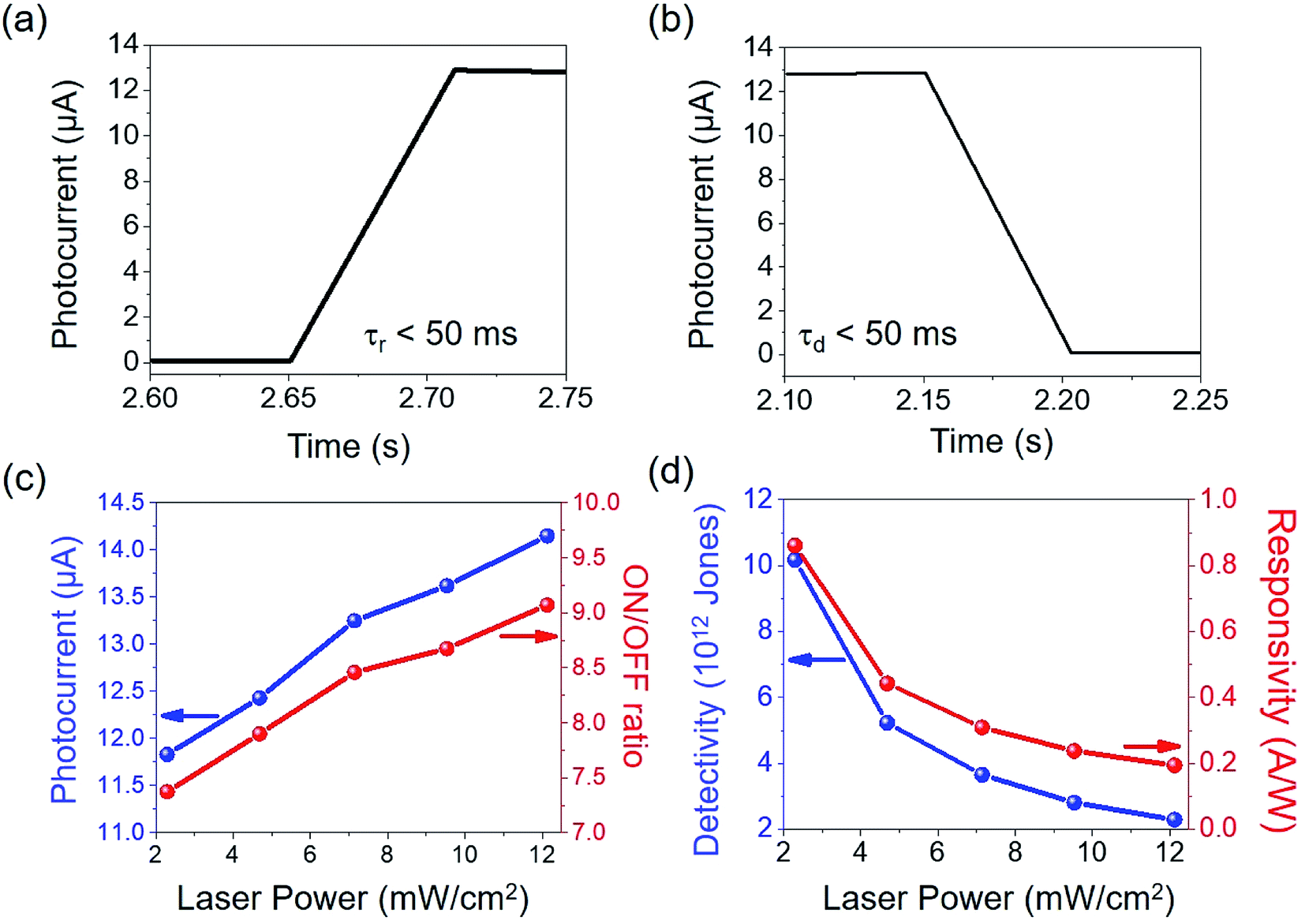 | ||
| Fig. 5 Photocurrent-time graphs at laser power Plaser of ∼12.13 mW cm−2 to show (a) rise time τr and (b) decay time τd. The average τr and τd were less than 50 ms for the inkjet printed graphene–WS2–graphene heterostructure device. (c) Variation of photocurrent Ip, and ON/OFF ratio with applied laser power Plaser. Photocurrent and ON/OFF ratio increased with an increase in input voltage or applied laser power due to the higher flow of charge carriers. (d) Detectivity D, and responsivity R, as a function of laser power Plaser. The D and R decrease inversely with Plaser, consistent with eqn (1) and (2). | ||
Capacitance–voltage (C–V) measurements were also conducted to study the nature of the graphene (M)–WS2 (S) interface. The voltage applied was across two graphene contacts by placing probe tips on these pads, as illustrated in Fig. 6(a). The C was measured as a function of bias voltage V using the Keysight B1500A semiconductor device analyzer with the multi-frequency CMU B1520A unit attached. As stated previously, the non-linearity in the Id–V measurement is attributed to the Schottky diode-type behavior of the graphene–WS2 interfacial junction. Therefore, two Schottky diodes are in series with each other in the inkjet printed graphene–WS2–graphene heterostructure device. Fig. 6(b) shows the rise and fall in C at various frequencies ranging from 20 kHz up to 3 MHz, while V was swept from −6 V to 6 V. The initial rise in C with V is attributed to the formation of a Schottky barrier against electron flow at the graphene–WS2 interface. Capacitance remains constant up to a certain bias voltage and then it decreases. The subsequent fall in C is attributed to the removal or reduction of the Schottky barrier at the WS2–graphene interface, where the magnitude of C is dependent on the filling and refilling of trap states by the charge carriers.52,53 Highest C values were measured at 20 kHz and at 0 V, where a value of ∼324.88 pF was tabulated, while the lowest C of ∼2.81 pF was measured at the highest f of ∼3 MHz and 0 V. The C–V measurements help in deciphering the depletion region and in predicting the charging and discharging of capacitance54,55
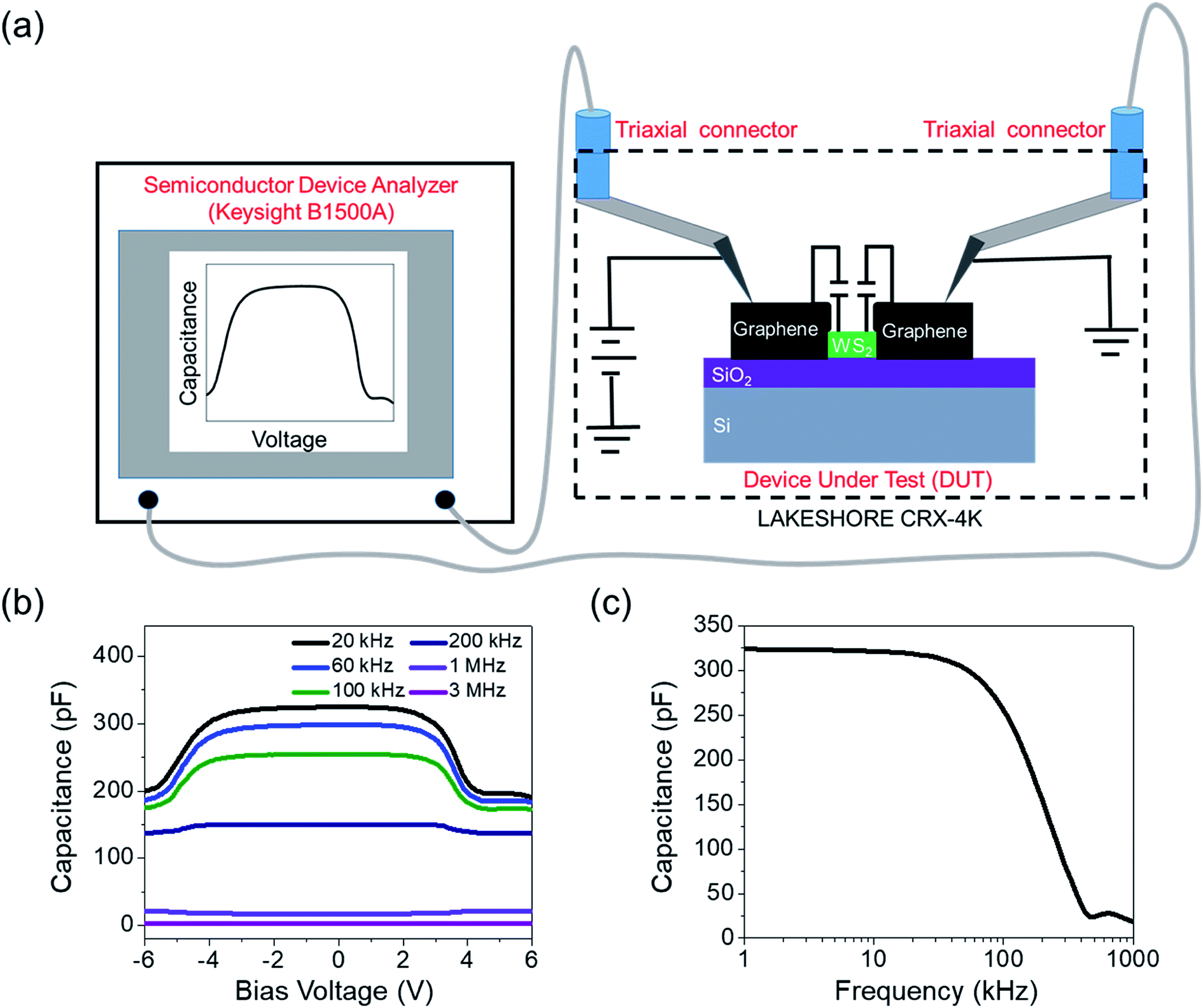 | ||
| Fig. 6 (a) Capacitance–voltage–frequency (C–V–f) measurement setup to study the graphene–WS2 and WS2–graphene interface characteristics. The inkjet-printed graphene–WS2–graphene heterostructure device enacts the behavior of two Schottky diodes in series with each other. The graphene–WS2 junction showed a non-ohmic rectifying behavior suggestive of its Schottky diode type behavior. (b) Capacitance at various frequencies as a function of bias voltage. The C–V measurements exploit the formation of the depletion region and charging and discharging of capacitance formed within the junction. (c) Capacitance–frequency measurement demonstrating the strong dependence of capacitance with frequency. The decrease in capacitance with frequency is accredited to reduction or annihilation of interface trapped states. | ||
From the data in Fig. 6(c), when the frequency f applied is significantly low, a higher value of C is observed because of the extra capacitance offered by interface trapped states. The fall in C with increasing f (>100 kHz) is due to a decrease in the Schottky barrier height. No significant change in C was observed for f > 200 kHz, indicating the absence of a barrier against electron flow. Thus, the C–f measurements in Fig. 6(c) show the sharp decrease in capacitance from ∼315.75 pF at 25.76 kHz to ∼23.79 pF at 480 kHz frequency, indicating a strong frequency effect on capacitance built-up at the graphene–WS2 interface. The decrease in C with increasing f is attributed to the fact that a fewer number of electrons are trapped in the interface states, owing to a decrease in the Schottky barrier height and after a certain f, their contribution toward the C formation is almost negligible. These results suggest that inkjet printed 2D semiconducting WS2 and conducting graphene layered materials formed using HT sonication show promise for the design of devices and components in RF and microwave engineering for future applications.
3. Conclusions
In summary, our work has revealed that HT sonication offered electrical conductivities higher than obtained by SM but lower than those obtained by MS, while providing the highest stability when compared to the other two techniques for formulating dispersions of semiconducting WS2. From this work, the inkjet printed graphene–WS2–graphene heterostructure devices were constructed using HT sonication. The non-ohmic I–V for the inkjet printed graphene–WS2–graphene heterostructure device indicated a Schottky diode type behavior where the optoelectronic properties were promising and yielded a maximum R of ∼0.86 A W−1, D ∼ 1013 Jones, while τr and τd were <50 ms. The C–V measurements at various frequencies showed the rise and fall in capacitance values which is attributed to the formation and depletion of the Schottky barrier at the graphene–WS2 and WS2–graphene interfaces, respectively. The C obtained was as high as ∼324.88 pF at frequencies of ∼20 kHz, while it decreased down to ∼2.81 pF for frequencies as high as 3 MHz.4. Experimental
Cyclohexanone (70%) (Sigma Aldrich # 398241)/terpineol (30%) (Sigma Aldrich # 86480) solution (C/T) mixtures were prepared in glass vials. Ethyl cellulose, EC (2.5 weight%) (Sigma Aldrich # 200646) was then added to the solution and bath sonicated for 2 hours to ensure complete dissolution of EC in the C/T solution mixture. This particular combination of C/T/EC was used because it has a viscosity of about ∼12 cP which is ideal for inkjet printing, as reported in our previous work.56,57 The WS2 powder (Sigma Aldrich # 243639) was used at a concentration of 30 mg ml−1 for all our experiments.For MS, the WS2 powder was taken in two separate glass vials and 5 ml of C/T/EC solution mixture was then added to each vial. A magnetic stir bar was then put in both glass vials. One vial was magnetically stirred at 100 rpm (MS (low)), while another vial was stirred at 1500 rpm (MS (high)) for 24 hours to generate the dispersion.
For SM, the WS2 powder was taken in two separate glass beakers and 50 ml of C/T/EC solution mixture was then added as previously. This was the minimum amount of solution required for using our shear mixer. Lowest speed of 2500 rpm (SM (low)) and the highest speed of 6000 rpm (SM (high)) was used for 5 hours of shear mixing. These parameters were established to achieve uniform mixing while minimizing overheating.
For HT sonication, the WS2 powder was taken in two separate glass beakers and 20 ml of C/T/EC solution mixture was again added. This was the minimum amount of solution required for horn-tip sonication. A minimum power amplitude of 20% (HT (low)) and a maximum of 40% (HT (high)) was used for 3 hours. Pulse ON and OFF times were 30 seconds each, respectively, and the total sonication time was 6 hours. The parameters for sonication was also chosen such that it was performed at room temperature without overheating the samples.
Extreme parameters are used for all three methods with liquid-phase exfoliation to optimize the conditions for yielding semiconducting WS2 nanosheets that are stable for at least one month. One drop of each sample was cast on a SiO2/Si wafer using a plastic pipette. Annealing was performed at 250 °C for 2 hours to ensure complete desorption of the solvent. The Fujifilm DMP-2800 series Dimatix Material Printer consisting of 16 inkjet nozzles were used to print graphene–WS2–graphene heterostructure devices discussed in this work. A cartridge temperature of ∼40 °C and a platen temperature of 60 °C were used for printing. Raman spectroscopy was performed using a Horiba LabRAM HR Evolution Microscope. Electrical characterization was performed using a micromanipulator 450PM-B probe stage equipped with an Agilent 4156A precision semiconductor parameter analyzer. The Lakeshore CRX-4K, Agilent 33220A 20 MHz arbitrary waveform generator, Thorlabs laser source model S1FC660 and Keysight B1500 semiconductor device analyzer with attached Keysight medium power SMU B1511B unit, were used for the Id–V and Ip measurements. The Lakeshore CRX-4K and Keysight B1500 semiconductor device analyzer with attached Keysight multi-frequency CMU B1520A unit were used for the C–V–f measurements of the graphene–WS2–graphene devices.
Conflicts of interest
There are no conflicts to declare.Acknowledgements
We greatly appreciate the support received from the Army Research Office (grant number W911NF-15-1-0425) that enabled us to pursue this work. A. B. K. is also grateful to the support received from the UNT start-up package for helping establish the Nanoscale Materials and Devices Laboratory and the PACCAR Endowed Professorship and Institute support.References
- K. S. Novoselov, A. K. Geim, S. V. Morozov, D. A. Jiang, Y. Zhang, S. V. Dubonos, I. V. Grigorieva and A. A. Firsov, Electric field effect in atomically thin carbon films, Science, 2004, 306(5696), 666–669 CrossRef CAS PubMed.
- K. S. Novoselov, D. Jiang, F. Schedin, T. J. Booth, V. V. Khotkevich, S. V. Morozov and A. K. Geim, Two-dimensional atomic crystals, Proc. Natl. Acad. Sci. U. S. A., 2005, 102(30), 10451–10453 CrossRef CAS PubMed.
- A. B. Kaul, Two-dimensional layered materials: Structure, properties, and prospects for device applications, J. Mater. Res., 2014, 29(3), 348–361 CrossRef CAS.
- A. J. Chaves, R. M. Ribeiro, T. Frederico and N. M. R. Peres, Excitonic effects in the optical properties of 2D materials: an equation of motion approach, 2D Materials, 2017, 4(2), 025086 CrossRef.
- J. H. Kim, J. H. Jeong, N. Kim, R. Joshi and G.- H Lee, Mechanical properties of two-dimensional materials and their applications, J. Phys. D: Appl. Phys., 2018, 52(8), 083001 CrossRef.
- J. Kim, S. Byun, A. J. Smith, J. Yu and J. Huang, Enhanced electrocatalytic properties of transition-metal dichalcogenides sheets by spontaneous gold nanoparticle decoration, J. Phys. Chem. Lett., 2013, 4(8), 1227–1232 CrossRef CAS PubMed.
- K. F. Mak, C. Lee, J. Hone, J. Shan and T. F. Heinz, Atomically thin MoS2: a new direct-gap semiconductor, Phys. Rev. Lett., 2010, 105(13), 136805 CrossRef PubMed.
- W. Zhao, Z. Ghorannevis, L. Chu, M. Toh, C. Kloc, P.-H. Tan and G. Eda, Evolution of electronic structure in atomically thin sheets of WS2 and WSe2, ACS Nano, 2012, 7(1), 791–797 CrossRef PubMed.
- Q. H. Wang, K. Kalantar-Zadeh, A. Kis, J. N. Coleman and M. S. Strano, Electronics and optoelectronics of two-dimensional transition metal dichalcogenides, Nat. Nanotechnol., 2012, 7(11), 699–712 CrossRef CAS PubMed.
- M. Ye, D. Winslow, D. Zhang, R. Pandey and Y. Yap, Recent advancement on the optical properties of two-dimensional molybdenum disulfide (MoS2) thin films, Photonics, 2015, 2(1), 288–307 CrossRef CAS.
- M.-S. Alejandro, K. Hummer and L. Wirtz, Vibrational and optical properties of MoS2: From monolayer to bulk, Surf. Sci. Rep., 2015, 70(4), 554–586 CrossRef.
- D. Lembke, S. Bertolazzi and A. Kis, Single-layer MoS2 electronics, Acc. Chem. Res., 2015, 48(1), 100–110 CrossRef CAS PubMed.
- E. Yalon, C. J. McClellan, K. K. H. Smithe, M. M. Rojo, R. L. Xu, S. V. Suryavanshi, A. J. Gabourie, C. M. Neumann, F. Xiong, A. B. Farimani and E. Pop, Energy dissipation in monolayer MoS2 electronics, Nano Lett., 2017, 17(6), 3429–3433 CrossRef CAS PubMed.
- G. Eda, T. Fujita, H. Yamaguchi, D. Voiry, M. Chen and M. Chhowalla, Coherent atomic and electronic heterostructures of single-layer MoS2, ACS Nano, 2012, 6(8), 7311–7317 CrossRef CAS PubMed.
- S. H. Lee, D. Lee, W. S. Hwang, E. Hwang, D. Jena and W. J. Yoo, High-performance photocurrent generation from two-dimensional WS2 field-effect transistors, Appl. Phys. Lett., 2014, 104(19), 193113 CrossRef.
- A. S. Pawbake, R. G. Waykar, D. J. Late and S. R. Jadkar, Highly transparent wafer-scale synthesis of crystalline WS2 nanoparticle thin film for photodetector and humidity-sensing applications, ACS Appl. Mater. Interfaces, 2016, 8(5), 3359–3365 CrossRef CAS PubMed.
- N. Perea-López, A. L. Elías, A. Berkdemir, A. Castro-Beltran, H. R. Gutiérrez, S. Feng and R. Lv, Photosensor device based on few-layered WS2 films, Adv. Funct. Mater., 2013, 23(44), 5511–5517 CrossRef.
- H.-S. Kim, M. Patel, J. Kim and M. S. Jeong, Growth of Wafer-Scale Standing Layers of WS2 for Self-Biased High-Speed UV–Visible–NIR Optoelectronic Devices, ACS Appl. Mater. Interfaces, 2018, 10(4), 3964–3974 CrossRef CAS PubMed.
- D. Ovchinnikov, A. Allain, Y.-S. Huang, D. Dumcenco and A. Kis, Electrical transport properties of single-layer WS2, ACS Nano, 2014, 8(8), 8174–8181 CrossRef CAS PubMed.
- M. Buscema, J. O. Island, D. J. Groenendijk, S. I. Blanter, G. A. Steele, H. S. J van der Zant and A. Castellanos-Gomez, Photocurrent generation with two-dimensional van der Waals semiconductors, Chem. Soc. Rev., 2015, 44(11), 3691–3718 RSC.
- H. Chen, H. Liu, Z. Zhang, K. Hu and X. Fang, Nanostructured photodetectors: from ultraviolet to terahertz, Adv. Mater., 2016, 28(3), 403–433 CrossRef CAS PubMed.
- C. Li, C. Han, Y. Zhang, Z. Zang, M. Wang, X. Tang and J. Du, Enhanced photoresponse of self-powered perovskite photodetector based on ZnO nanoparticles decorated CsPbBr3 films, Sol. Energy Mater. Sol. Cells, 2017, 172, 341–346 CrossRef CAS.
- Q. Ou, Y. Zhang, Z. Wang, J. A. Yuwono, R. Wang, Z. Dai, W. Li, C. Zheng, Z.-Q. Xu, X. Qi, S. Duhm, N. V. Medhekar, H. Zhang and Q. Bao, “Strong Depletion in Hybrid Perovskite p–n Junctions Induced by Local Electronic Doping, Adv. Mater., 2018, 30(15), 1705792 CrossRef PubMed.
- Y. Zhang, C.-K. Lim, Z. Dai, G. Yu, J. W. Haus, H. Zhang and P. N. Prasad, Photonics and optoelectronics using nano-structured hybrid perovskite media and their optical cavities, Phys. Rep., 2019, 795, 1–51 CrossRef CAS.
- H. Guo, C. Lan, Z. Zhou, P. Sun, D. Wei and C. Li, Transparent, flexible, and stretchable WS2 based humidity sensors for electronic skin, Nanoscale, 2017, 9(19), 6246–6253 RSC.
- A. S. Pawbake, R. G. Waykar, D. J. Late and S. R. Jadkar, Highly transparent wafer-scale synthesis of crystalline WS2 nanoparticle thin film for photodetector and humidity-sensing applications, ACS Appl. Mater. Interfaces, 2016, 8(5), 3359–3365 CrossRef CAS PubMed.
- A. S. Aji, P. Solís-Fernández, H. G. Ji, K. Fukuda and H. Ago, High Mobility WS2 Transistors Realized by Multilayer Graphene Electrodes and Application to High Responsivity Flexible Photodetectors, Adv. Funct. Mater., 2017, 27(47), 1703448 CrossRef.
- Y. Yu, Y. Zhang, X. Song, H. Zhang, M. Cao, Y. Che, H. Dai, J. Yang, H. Zhang and J. Yao, PbS-decorated WS2 phototransistors with fast response, ACS Photonics, 2017, 4(4), 950–956 CrossRef CAS.
- M. Hirano and S. Miyake, Sliding life enhancement of a WS2 sputtered film by ion beam mixing, Appl. Phys. Lett., 1985, 47(7), 683–685 CrossRef CAS.
- C. Cong, J. Shang, X. Wu, B. Cao, N. Peimyoo, C. Qiu, L. Sun and T. Yu, Synthesis and optical properties of large-area single-crystalline 2D semiconductor WS2 monolayer from chemical vapor deposition, Adv. Opt. Mater., 2014, 2(2), 131–136 CrossRef.
- Y. Niu, S. Gonzalez-Abad, R. Frisenda, P. Marauhn, M. Drüppel, P. Gant, R. Schmidt, N. S. Taghavi, D. Barcons, A. J. Molina-Mendoza, S. M. de Vasconcellos, R. Bratschitsch, D. P. De Lara, M. Rohlfing and A. Castellanos-Gomez, Thickness-Dependent Differential Reflectance Spectra of Monolayer and Few-Layer MoS2, MoSe2, WS2 and WSe2, Nanomaterials, 2018, 8(9), 725 CrossRef PubMed.
- J. A. Desai, N. Adhikari and A. B. Kaul, Tungsten Disulfide Nanodispersions for Inkjet Printing and Semiconducting Devices, MRS Adv., 2017, 2(60), 3691–3696 CrossRef CAS.
- D. Fadil, R. F. Hossain, G. A. Saenz and A. B. Kaul, On the chemically-assisted excitonic enhancement in environmentally-friendly solution dispersions of two-dimensional MoS2 and WS2, J. Mater. Chem. C, 2017, 5(22), 5323–5333 RSC.
- A. Delgado, J. A. Catalan, H. Yamaguchi, C. N. Villarrubia, A. D. Mohite and A. B. Kaul, Characterization of 2D MoS2 and WS2 Dispersed in Organic Solvents for Composite Applications, MRS Adv., 2016, 1(32), 2303–2308 CrossRef CAS.
- V. Nicolosi, M. Chhowalla, M. G. Kanatzidis, M. S. Strano and J. N. Coleman, Liquid exfoliation of layered materials, Science, 2013, 340(6139), 1226419 CrossRef.
- S. Pang, H. N. Tsao, X. Feng and K. Müllen, Patterned graphene electrodes from solution-processed graphite oxide films for organic field-effect transistors, Adv. Mater., 2009, 21(34), 3488–3491 CrossRef CAS.
- M. Michel, C. Biswas and A. B. Kaul, High-performance ink-jet printed graphene resistors formed with environmentally-friendly surfactant-free inks for extreme thermal environments, Appl. Mater. Today, 2017, 6, 16–21 CrossRef.
- R. F. Hossain, I. G. Deaguero, T. Boland and A. B. Kaul, Biocompatible, large-format, inkjet printed heterostructure MoS2-graphene photodetectors on conformable substrates, npj 2D Mater. Appl., 2017, 1(1), 28 CrossRef.
- L. M. Malard, M. A. Pimenta, G. Dresselhaus and M. S. Dresselhaus, Raman spectroscopy in graphene, Phys. Rep., 2009, 473(5–6), 51–87 CrossRef CAS.
- S. Sakamoto, M. Okumura, Z. Zhao and Y. Furukawa, Raman spectral changes of PEDOT–PSS in polymer light-emitting diodes upon operation, Chem. Phys. Lett., 2005, 412(4), 395–398 CrossRef CAS.
- M. Thripuranthaka, R. V. Kashid, C. S. Rout and D. J. Late, Temperature-dependent Raman spectroscopy of chemically derived few-layer MoS2 and WS2 nanosheets, Appl. Phys. Lett., 2014, 104(8), 081911 CrossRef.
- G. L. Frey, R. Tenne, M. J. Matthews, M. S. Dresselhaus and G. Dresselhaus, Optical properties of MS2 (M = Mo, W) inorganic fullerene like and nanotube material optical absorption and resonance Raman measurements, J. Mater. Res., 1998, 13(9), 2412–2417 CrossRef CAS.
- R. K. Jha and P. K. Guha, Liquid exfoliated pristine WS2 nanosheets for ultrasensitive and highly stable chemiresistive humidity sensors, Nanotechnology, 2016, 27(47), 475503 CrossRef PubMed.
- A. Splendiani, L. Sun, Y. Zhang, T. Li, J. Kim, C.-Y. Chim, G. Galli and F. Wang, Emerging photoluminescence in monolayer MoS2, Nano Lett., 2010, 10(4), 1271–1275 CrossRef CAS PubMed.
- H. Tan, Y. Fan, Y. Zhou, Q. Chen, W. Xu and J. H. Warner, Ultrathin 2D photodetectors utilizing chemical vapor deposition grown WS2 with graphene electrodes, ACS Nano, 2016, 10(8), 7866–7873 CrossRef CAS PubMed.
- A. Allain, J. Kang, K. Banerjee and A. Kis, Electrical contacts to two-dimensional semiconductors, Nat. Mater., 2015, 14(12), 1195 CrossRef CAS PubMed.
- S. Mazumder, A. Delgado, J. A. Catalan, H. Yamaguchi, C. N. Villarrubia, A. D. Mohite and A. B. Kaul, Opto-electro-mechanical percolative composites from 2D layered materials: properties and applications in strain sensing, Compos. Sci. Technol., 2019, 182, 107687 CrossRef.
- J. A. Desai, S. Chugh, M. Michel and A. B. Kaul, Inkjet printed graphene as an interconnect for optoelectronic devices, J. Mater. Sci.: Mater. Electron., 2019, 30(13), 1–10 CrossRef.
- T.-F. Zhang, Z.-P. Li, J.-Z. Wang, W.-Y. Kong, G.-A. Wu, Y.-Z. Zheng, Y.-W. Zhao, E.-X. Yao, N.-X. Zhuang and L.-B. Luo, Broadband photodetector based on carbon nanotube thin film/single layer graphene Schottky junction, Sci. Rep., 2016, 6, 38569 CrossRef CAS PubMed.
- C. Zhang, S. Wang, L. Yang, Y. Liu, T. Xu, Z. Ning, A. Zak, Z. Zhang, R. Tenne and Q. Chen, High-performance photodetectors for visible and near-infrared lights based on individual WS2 nanotubes, Appl. Phys. Lett., 2012, 100(24), 243101 CrossRef.
- N. Huo, S. Yang, Z. Wei, S.-S. Li, J.-B. Xia and J. Li, Photoresponsive and gas sensing field-effect transistors based on multilayer WS2 nanoflakes, Sci. Rep., 2014, 4, 5209 CrossRef CAS PubMed.
- A. Zylbersztejn, Trap depth and electron capture cross section determination by trap refilling experiments in Schottky diodes, Appl. Phys. Lett., 1978, 33(2), 200–202 CrossRef CAS.
- I. Hussain, M. Y. Soomro, N. Bano, O. Nur and M. Willander, Interface trap characterization and electrical properties of Au-ZnO nanorod Schottky diodes by conductance and capacitance methods, J. Appl. Phys., 2012, 112(6), 064506 CrossRef.
- N. Adhikari, A. Bandyopadhyay and A. Kaul, Nanoscale Characterization of WSe2 for Opto-electronics Applications, MRS Adv., 2017, 2(60), 3715–3720 CrossRef CAS.
- L. Peng, X. Peng, B. Liu, C. Wu, Y. Xie and G. Yu, Ultrathin two-dimensional MnO2/graphene hybrid nanostructures for high-performance, flexible planar supercapacitors, Nano Lett., 2013, 13(5), 2151–2157 CrossRef CAS PubMed.
- M. Michel, J. A. Desai, A. Delgado, C. Biswas and A. B. Kaul, Optimization of fluid characteristics of 2D materials for inkjet printing, MRS Adv., 2016, 1(30), 2199–2206 CrossRef CAS.
- M. Michel, J. A. Desai, C. Biswas and A. B. Kaul, Engineering chemically exfoliated dispersions of two-dimensional graphite and molybdenum disulfide for ink-jet printing, Nanotechnology, 2016, 27(48), 485602 CrossRef PubMed.
| This journal is © The Royal Society of Chemistry 2019 |