
 Open Access Article
 This Open Access Article is licensed under a Creative Commons Attribution-Non Commercial 3.0 Unported Licence
Optical and electrical properties of all-inorganic Cs2AgBiBr6 double perovskite single crystals
Zheng Zhang a,
Ge Yang*a,
Chuanzhen Zhoub,
Ching-Chang Chungb and
Ibrahim Hanya
a,
Ge Yang*a,
Chuanzhen Zhoub,
Ching-Chang Chungb and
Ibrahim Hanya
aDepartment of Nuclear Engineering, North Carolina State University, Raleigh, North Carolina 27695-7909, USA. E-mail: gyang9@ncsu.edu
bAnalytical Instrumentation Facility, North Carolina State University, Raleigh, North Carolina 27695-7531, USA
First published on 29th July 2019
Abstract
In this work, we explored the possibility of using Cs2AgBiBr6, a double perovskite crystal, for radiation detection. Cs2AgBiBr6 crystals were grown using the solution growth technique. The resistivity of the as-grown Cs2AgBiBr6 crystal is larger than 1010 Ω cm, which is high enough to ensure low leakage current for fabrication of semiconductor radiation detectors. Using the temperature-dependent resistivity measurements, we estimated that the Fermi level is at 0.788 eV above the valence band and the material is a p-type semiconductor. From the low-temperature cathodoluminescence measurements, two near band gap energies at 1.917 eV and 2.054 eV were revealed.
High performance radiation detectors are widely sought after in many fields, such as national security defense, medical imaging, astrophysical study, industrial monitoring, and basic scientific research.1–7 As the core component of detector systems, the detection material plays a key role in determining the ultimate device performance. In the past few years, many candidate materials, especially single crystals, have been investigated for radiation detection applications.2,4,6,7 Even though some of the candidate crystals have achieved success to different extents, many limitations remain untackled. For example, high-purity germanium (HPGe) detectors can offer a superior energy resolution,8 but HPGe needs to be cryogenically cooled for routine detector operation. The existence of the bulky cooling system makes HPGe detectors inappropriate for many applications.9 Cadmium zinc telluride (CdZnTe) crystals are currently one of the leading semiconductors for room-temperature X-ray and gamma-ray detection. They can provide high energy resolution and high charge collection efficiency without the need for cryogenic cooling. However, the material non-uniformity and the relatively high cost need to be further addressed to promote its large-scale deployment.7 Owing to the limitations of existing semiconductor crystals, there is consistently a need for exploring new room-temperature semiconductor-based radiation detector materials. The ideal candidate materials should overcome the aforementioned drawbacks. Simultaneously, this material should be applicable with a low fabrication cost for large-scale deployment.
Among the promising candidates, perovskite crystals, which share the structure ABX3 (e.g., A = methylammonium (MA) or formamidinium (FA), B = Pb2+, X = Br−, Cl−, I−), have started to attract interests from the radiation detection community. This type of material has been widely investigated in the area of solar cells over the past few years.10–18 These efforts have revealed that perovskite crystals have many attractive characteristics, such as high resistivity, large lifetime (τ)–mobility (μ) product, good thermal stability, and low fabrication cost using solution processing methods. These characteristics offer ideal bases for fabricating high performance and cost-friendly radiation devices. However, one major issue related with the development of hybrid (organic–inorganic) perovskite is the long-term instability. MA-based lead halide compounds present better stability in air over months,19 while FA-based perovskites can undergo phase change within days or even hours.17 It is known that air exposure may not be the direct driving force for performance degradation of perovskites, but it can accelerate the perovskite decomposition process.34 In this regard, the inorganic perovskites exhibits better long term stability than its hybrid counterparts. Therefore, the inorganic perovskites (e.g., CsPbBr3 and CsPbI2Br) possess great potential as high performance radiation detector materials for long-term practical use.35
To further explore the possibility of using perovskites for radiation detection, we studied an inorganic double perovskite single crystal Cs2AgBiBr6 in this work. This material was chosen for the following reasons: Firstly, Cs2AgBiBr6 has large average atomic number (Cs = 55, Ag = 47, Bi = 83) and high density (4.65 g cm−3). Large average atomic number implies high mass attenuation coefficients, which is especially important for the development of X-ray and gamma-ray radiation detectors. The attenuation capability of Cs2AgBiBr6 is comparable to CdZnTe and CdTe as can be seen in Fig. 1 (data is available online in XCOM photon cross section database). High density leads to a much larger intrinsic efficiency, which is defined as the ratio of counts under the photo-peak to the photons interacting with the detector. Secondly, previously reported humidity and thermal stability tests confirmed the high moisture and heat resistance capabilities of Cs2AgBiBr6,20 which offer potential for long-term and stable device operation. More importantly, this crystal does not contain lead, which eliminates the use of toxic heavy metal in the case of hybrid lead halide perovskites. We note the solubility constant of AgBr is approximately four orders of magnitude lower than that of PbI2.21 Finally, previous work by Hoye et al. indicated fundamental carrier lifetime in Cs2AgBiBr6 thin films can exceed 1 μs, which is even longer than the carrier lifetime in FAPbI3 and CdTe bulk single crystals (484 ns and ∼150 ns respectively).10,24,33 In this work, we grew the Cs2AgBiBr6 single crystals and performed detailed structural-, electrical- and optical measurements on as-grown crystals. We report these findings and analyze their correlation with the device performance.
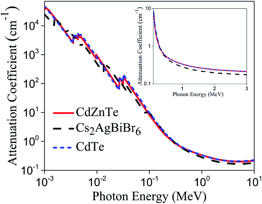 | ||
| Fig. 1 Attenuation coefficient of CdZnTe, Cs2AgBiBr6, and CdTe crystals as a function of photon energy, from X-ray to high energy gamma rays. Inset plot shows the attenuation coefficient as a function of photon energy, from 0.1 MeV to 3 MeV. | ||
The crystal growth was started by first dissolving 2.0 mmol CsBr (99.999%, Sigma Aldrich) and 1.0 mmol BiBr3 (99.999%, Sigma Aldrich) in HBr acid (99.9999%, 48% w/w, Alfa Aesar) at room temperature. AgBr (99.998%, Alfa Aesar) was then added and the solution was briefly stirred. Then the vial containing this solution was heated to 120 °C and maintained at this temperature until the solution was clear and transparent. The temperature was then decreased at a controlled rate of 2 °C h−1.22 The solution temperature was unchanged overnights to promote the crystal growth. This process generally takes 4 days to complete. Once the crystal growth ends, the solution was filtered using polytetrafluoroethylene (PTFE) filters. The as-grown crystals were carefully handled and washed using ethanol to remove chemical residues on the surface. In this work, a crystal in one centimeter size was able to be synthesized, however its shape was irregular.
X-ray diffraction (XRD) experiment was carried out using a rigaku SmartLab X-ray diffractometer with CuKα X-ray source. We observed the peaks from one set of parallel lattice planes from the typical as-grown bulk single crystal. The obtained diffraction pattern shown in Fig. 2a matches well with Cs2AgBiBr6 reference pattern in the database (ICSD collection #252164). This confirms that the as-grown crystals in our solution growth process is indeed Cs2AgBiBr6 phase.
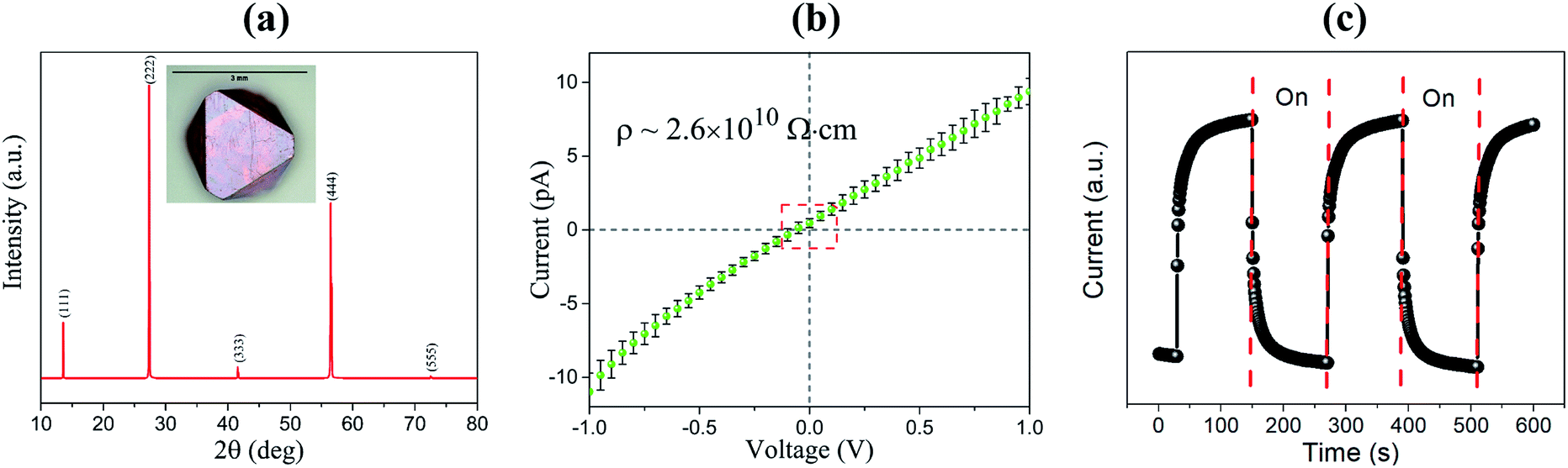 | ||
| Fig. 2 (a) X-ray diffraction (XRD) pattern of Cs2AgBiBr6 single crystal grown with our solution process. The inset is a picture of a typical as-grown single crystal. (b) Current–voltage (I–V) curve of Cs2AgBiBr6. Measurement was conducted at room temperature. Note the curve does not pass origin, probably indicating the existence of weak Schottky barrier. (c) Response of Cs2AgBiBr6 single crystals to LED light (wavelength: 472 nm), bias voltage: −5 V. | ||
For radiation detector applications, high resistivity of candidate semiconductor materials is an essential requirement since that ensures less leakage current, and ultimately, lower detector noise. Fig. 2b shows the current–voltage (I–V) characteristic of our Cs2AgBiBr6 crystal. Silver metal contacts were used as electrodes for Cs2AgBiBr6, which shows a good ohmic behavior. The corresponding resistivity is approximately 2.6 × 10¹⁰ Ω cm at room temperature. This is comparable with that of today's leading room-temperature radiation detector material CdZnTe. Fig. 2c presents the conductivity response of Cs2AgBiBr6 to 472 nm LED light. The high resistivity from our as-grown Cs2AgBiBr6 in combination with the high photo-response to LED light shows great potential to further explore device fabrication with these crystals.
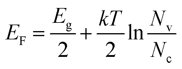
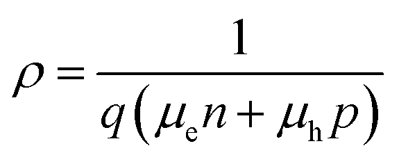
We measured the I–V characteristic of Cs2AgBiBr6 crystal at various temperatures and plotted the temperature dependence of the resistivity, as shown in Fig. 3a and b. The resistivity plot in Fig. 3b presents the classical semiconductor behaviors. In other words, the resistivity will decrease with the increase of temperature owing to the presence of more thermally excited carriers. Temperature-dependent resistivity can also help determine the Fermi level. The Fermi level position serves as a good indicator of the n-type or p-type nature of semiconductors. In intrinsic or pure semiconductors (equal concentration of electrons and holes), the position of Fermi level is given by
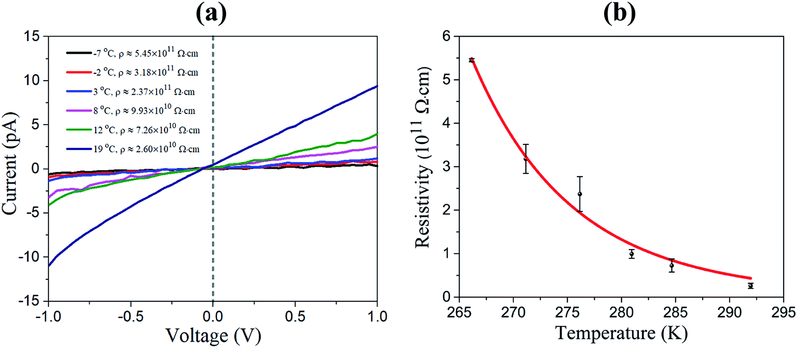 | ||
| Fig. 3 (a) I–V curves at different temperatures. (b) Crystal resistivity vs. temperature. | ||
Using the obtained temperature-dependent resistivity data, we determined the Fermi level position to be either 0.788 eV below the conduction band (n-type) or above the valence band (p-type), as shown in Fig. 4a and b. N. Guechi et al. reported that Cs2AgBiBr6 has larger Nv compared with the magnitude of Nc,23 which would cause the Fermi level to shift up above the midgap if the material is intrinsic (which does not exist as real). However, this shift is small, as kT is roughly 0.025 eV compared with Eg which is approximately 2 eV as shown in our cathodoluminescence (CL) measurements. Thus, we reasoned the intrinsic defects have caused the difference between Fermi level position and midgap, which ultimately determines the conduction type of the crystal. The crystal defects could serve as traps for the movement of carriers, as revealed in the CL spectrum of Fig. 5. Specifically, more deep electron traps (e.g., antisite substitution BiAg and vacancy VBr) are likely present in Cs2AgBiBr6 single crystals compared with hole traps.32 The above results indicate that as-grown Cs2AgBiBr6 is probably a p-type semiconductor, which is consistent with some previously published works.24,25
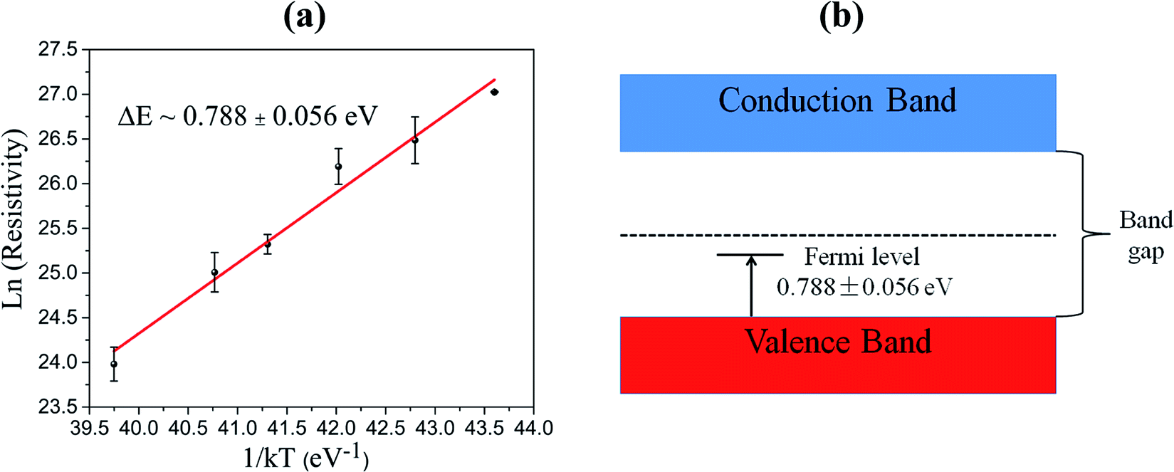 | ||
| Fig. 4 (a) Temperature dependence of the resistivity for Fermi level determination. (b) Relative Fermi level position in the forbidden band. | ||
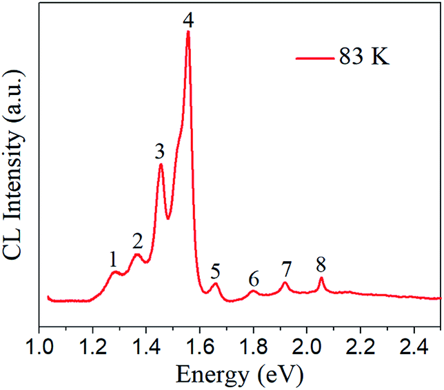 | ||
| Fig. 5 CL spectrum of Cs2AgBiBr6 single crystal. | ||
Fig. 5 presents the low-temperature CL spectrum of Cs2AgBiBr6, measured at 83 K. Lozhkina et al. determined the approximate band gap energies of Cs2AgBiBr6 to be 1.946 eV (indirect), 2.095 eV (indirect), and 2.254 eV (direct) from photoluminescence spectrum at T = 1.5 K.26 In the present study, the two peaks at 1.917 eV and 2.054 eV are ascribed to near band gap emissions with low intensities. They are likely from free exciton or bound exciton emissions, which can be induced when the created electrons and holes from band-gap radiation recombine and form free excitons, or the free excitons collide with donors or acceptors and bound to them to form (D+, X) or (A−, X) complexes.29 The two near band gap energies given in the CL spectrum are lower than the band gap of hybrid perovskite MAPbBr3 (2.21 eV) and MAPbCl3 (2.97 eV).12,27 Rest of the CL peaks (Table 1) likely come from the intrinsic material defects in the forbidden band. Some defects are CL emission activators and serve as recombination sites, which consequently produce photons in radioactive recombination processes. One example of such defects is the dislocations, which can induce localized electronic shallow levels due to the elastic strain fields and deep levels near middle of the gap because of the dangling bonds.28 Another possible defect, vacancies (e.g., VBr, VAg, VBi), can serve as donors (cation vacancy) or acceptors (anion vacancy).32,36 Recombination may occur at donor or acceptor energy levels (donor-to-valence or band-to-acceptor) and therefore luminescence are likely to occur. In other cases, a donor–acceptor (D–A) pair emission is possible when electrons bound to donors and holes bound to acceptors. The ambiguity will be further solved experimentally using the follow-on thermal annealing method.
| Peak number | Energy (eV) |
|---|---|
| 1 | 1.288 |
| 2 | 1.367 |
| 3 | 1.454 |
| 4 | 1.556 |
| 5 | 1.659 |
| 6 | 1.798 |
| 7 | 1.917 |
| 8 | 2.054 |
In summary, we grew and assessed the potential of double perovskite Cs2AgBiBr6 single crystals for optoelectronic device applications with a focus on radiation detection. The as-grown Cs2AgBiBr6 crystals have a resistivity > 1010 Ω cm, which is beneficial for reducing leakage current and performing room temperature X-ray and gamma-ray detection. We determined the Fermi level position in the forbidden band from temperature-dependent resistivity measurements, which indicated that this material is possibly a p-type semiconductor. The possible Fermi level pinning phenomenon can be further analyzed for the interpretation of deep level defects. The two near band gap energies determined from CL are 1.917 eV and 2.054 eV, which indicates that Cs2AgBiBr6 may be suitable for high energy photon detection. Finally, the CL spectrum revealed the presence of a series of deep-level defect traps. These defect traps serve as carrier recombination sites, which produce photons when excited electrons decay back to valence bands.
Methods
Current–voltage measurement and Fermi level
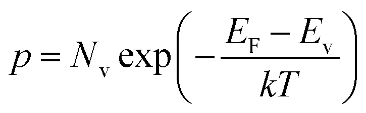
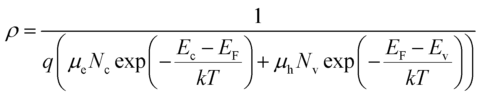
The current–voltage measurement was performed using the Keithley 6487 picoammeter/voltage source. Voltage was set from −1 V to 1 V with step 0.05 V and one second for each step. The pre-installed software in excel was used for initial picoammeter parameter settings.The Fermi level is a hypothetical energy level where electrons have 50% probability to occupy under thermodynamic equilibrium. For semiconductors, the resistivity ρ can be expressed in the following way,30,31
 | (1) |
In Boltzmann relations, the electron and hole concentrations are given by,
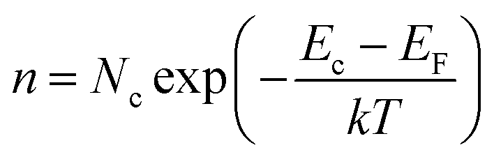 | (2) |
 | (3) |
Therefore, we can substitute eqn (2) and (3) into eqn (1),
 | (4) |
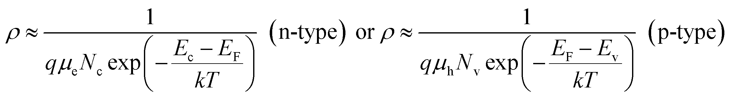
In p or n type semiconductors, there is large difference between carrier densities. Thus,
 | (5) |
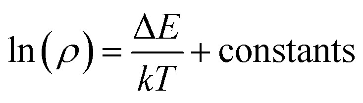
Additionally, since the temperature range is narrow (265 K to 295 K), Nc, Nv, μe, μh can be treated as constants with no variations. Therefore, by taking logarithmic transformation, the Fermi level position can be determined using,
 | (6) |
For p-type semiconductor, ΔE refers to the position of Fermi level above the valence band. For n-type semiconductor, ΔE refers to the position of Fermi level below the conduction band.
CL experiments
CL measurement was performed using the JEOL JSM-7600F Scanning Electron Microscope (SEM) coupled with a Horiba H-CLUE CL system (wide spectral range 200–2200 nm). The stage temperature was controlled by a cryo-stage with internal heater. We waited for 10 min to reach temperature equilibrium before CL measurement.Conflicts of interest
There are no conflicts of interest to declare.Acknowledgements
The work was partially supported by the U.S. Nuclear Regulatory Commission (NRC). The measurements were performed in part at the Analytical Instrumentation Facility (AIF) at North Carolina State University, which is supported by the State of North Carolina and the National Science Foundation (award number ECCS-1542015). The AIF is a member of the North Carolina Research Triangle Nanotechnology Network (RTNN), a site in the National Nanotechnology Coordinated Infrastructure (NNCI).References
- P. E. Vanier, Applications of Noble Gas Radiation Detectors to Counter-Terrorism, AIP Conf. Proc., 2003, 632, 37–45 CrossRef
.
- O. Mawlawi, Radiation Detectors for Medical Applications, J. Nucl. Med., 2008, 49, 1212 CrossRef
- P. Bennati, A. Dasu, M. Colarieti-Tosti, G. Lönn, D. Larsson, A. Fabbri, M. Galasso, M. N. Cinti, R. Pellegrini and R. Pani, Preliminary Study of a New Gamma Imager for On-Line Proton Range Monitoring during Proton Radiotherapy, J. Instrum., 2017, 12, C05009 CrossRef
- S. D. Sordo, L. Abbene, E. Caroli, A. M. Mancini, A. Zappettini and P. Ubertini, Progress in the Development of CdTe and CdZnTe Semiconductor Radiation Detectors for Astrophysical and Medical Applications, Sensors, 2009, 9, 3491–3526 CrossRef PubMed
- B. Seitz, N. Campos Rivera, R. Gray, A. Powell and F. Thomson, Radiation Sensors for Medical, Industrial and Environmental Applications: How to Engage with Schools and the General Public, Phys. Educ., 2017, 53, 014001 CrossRef
- S. Z. Lewin, Nuclear Radiation Detectors, J. Chem. Educ., 1961, 38, A135 CrossRef
- A. E. Bolotnikov, S. Babalola, G. S. Camarda, Y. Cui, S. U. Egarievwe, A. Hossain, G. Yang and R. B. James, Material Properties Limiting the Performance of CZT Gamma-Ray Detectors, 2009 Search PubMed
- G. F. Knoll, Radiation Detection and Measurement, John Wiley, 2010 Search PubMed
- M. T. Burks, O. B. Drury, J. O. Goldsten, D. J. Lawrence, P. N. Peplowski and Z. W. Yokley, Emerging Role of High-Purity Germanium Detectors for Planetary Science, 2018 Search PubMed
- Q. Han, S. H. Bae, P. Sun, Y. T. Hsieh, Y. Yang, Y. S. Rim, H. Zhao, Q. Chen, W. Shi and G. Li, et al., Single Crystal Formamidinium Lead Iodide (FAPbI3): Insight into the Structural, Optical, and Electrical Properties, Adv. Mater., 2016, 28, 2253–2258 CrossRef CAS PubMed
- Y. Rakita, N. Kedem, S. Gupta, A. Sadhanala, V. Kalchenko, M. L. Böhm, M. Kulbak, R. H. Friend, D. Cahen and G. Hodes, Low-Temperature Solution-Grown CsPbBr3 Single Crystals and Their Characterization, Cryst. Growth Des., 2016, 16, 5717–5725 CrossRef CAS
- D. Shi, V. Adinolfi, R. Comin, M. Yuan, E. Alarousu, A. Buin, Y. Chen, S. Hoogland, A. Rothenberger and K. Katsiev, et al., Low Trap-State Density and Long Carrier Diffusion in Organolead Trihalide Perovskite Single Crystals, Science, 2015, 347, 519–522 CrossRef CAS PubMed
- M. I. Saidaminov, M. A. Haque, J. Almutlaq, S. Sarmah, X.-H. Miao, R. Begum, A. A. Zhumekenov, I. Dursun, N. Cho and B. Murali, et al., Inorganic Lead Halide Perovskite Single Crystals: Phase-Selective Low-Temperature Growth, Carrier Transport Properties, and Self-Powered Photodetection, Adv. Opt. Mater., 2017, 5, 1600704 CrossRef
- M. I. Saidaminov, A. L. Abdelhady, B. Murali, E. Alarousu, V. M. Burlakov, W. Peng, I. Dursun, L. Wang, Y. He and G. Maculan, et al., High-Quality Bulk Hybrid Perovskite Single Crystals within Minutes by Inverse Temperature Crystallization, Nat. Commun., 2015, 6, 7586 CrossRef PubMed
- H. Zhang, X. Liu, J. Dong, H. Yu, C. Zhou, B. Zhang, Y. Xu and W. Jie, Centimeter-Sized Inorganic Lead Halide Perovskite CsPbBr3 Crystals Grown by an Improved Solution Method, Cryst. Growth Des., 2017, 17, 6426–6431 CrossRef CAS
- Q. Dong, Y. Fang, Y. Shao, P. Mulligan, J. Qiu, L. Cao and J. Huang, Electron-Hole Diffusion Lengths > 175 μm in Solution-Grown CH3NH3PbI3 Single Crystals, Science, 2015, 347, 967–970 CrossRef CAS PubMed
- A. A. Zhumekenov, M. I. Saidaminov, M. A. Haque, E. Alarousu, S. P. Sarmah, B. Murali, I. Dursun, X. H. Miao, A. L. Abdelhady and T. Wu, et al., Formamidinium Lead Halide Perovskite Crystals with Unprecedented Long Carrier Dynamics and Diffusion Length, ACS Energy Lett., 2016, 1, 32–37 CrossRef CAS
- Z. Lian, Q. Yan, T. Gao, J. Ding, Q. Lv, C. Ning, Q. Li and J. L. Sun, Perovskite CH3NH3PbI3(Cl) Single Crystals: Rapid Solution Growth, Unparalleled Crystalline Quality, and Low Trap Density toward 108 cm−3, J. Am. Chem. Soc., 2016, 138, 9409–9412 CrossRef CAS PubMed
- Y. Zhou, C. Li, Y. Wang, X. Du, P. Liu and W. Xie, Preparation and Characterization of High-Quality Perovskite CH3NH3PbX3 (I, Br) Single Crystal, IOP Conf. Ser.: Mater. Sci. Eng., 2017, 167, 012019 Search PubMed
- A. H. Slavney, R. W. Smaha, I. C. Smith, A. Jaffe, D. Umeyama and H. I. Karunadasa, Chemical Approaches to Addressing the Instability and Toxicity of Lead–Halide Perovskite Absorbers, Inorg. Chem., 2017, 56, 46–55 CrossRef CAS PubMed
- H. I. Karunadasa and A. H. Slavney, Halide Double Perovskite Cs2AgBiBr6 Solar-Cell Absorber Having Long Carrier Lifetimes, US Pat. application 20170194101, 2017
- A. H. Slavney, T. Hu, A. M. Lindenberg and H. I. Karunadasa, A Bismuth-Halide Double Perovskite with Long Carrier Recombination Lifetime for Photovoltaic Applications, J. Am. Chem. Soc., 2016, 138, 2138–2141 CrossRef CAS PubMed
- N. Guechi, A. Bouhemadou, S. Bin-Omran, A. Bourzami and L. Louail, Elastic, Optoelectronic and Thermoelectric Properties of the Lead-Free Halide Semiconductors Cs2AgBiX6 (X = Cl, Br): Ab Initio Investigation, J. Electron. Mater., 2018, 47, 1533–1545 CrossRef CAS
- R. L. Z. Hoye, L. Eyre, F. Wei, F. Brivio, A. Sadhanala, S. Sun, W. Li, K. H. L. Zhang, J. L. MacManus-Driscoll and P. D. Bristowe, et al., Fundamental Carrier Lifetime Exceeding 1 μs in Cs2AgBiBr6 Double Perovskite, Adv. Mater. Interfaces, 2018, 5, 1800464 CrossRef
- W. Pan, H. Wu, J. Luo, Z. Deng, C. Ge, C. Chen, X. Jiang, W. J. Yin, G. Niu and L. Zhu, et al., Cs2 AgBiBr6 Single-Crystal X-Ray Detectors with a Low Detection Limit, Nat. Photonics, 2017, 11, 726–732 CrossRef CAS
- O. A. Lozhkina, A. A. Murashkina, M. S. Elizarov, V. V. Shilovskikh, A. A. Zolotarev, Y. V. Kapitonov, R. Kevorkyants, A. V. Emeline and T. Miyasaka, Microstructural Analysis and Optical Properties of the Halide Double Perovskite Cs2BiAgBr6 Single Crystals, Chem. Phys. Lett., 2018, 694, 18–22 CrossRef CAS
- Y. Liu, Z. Yang, D. Cui, X. Ren, J. Sun, X. Liu, J. Zhang, Q. Wei, H. Fan and F. Yu, et al., Two-Inch-Sized Perovskite CH3NH3PbX3 (X = Cl, Br, I) Crystals: Growth and Characterization, Adv. Mater., 2015, 27, 5176–5183 CrossRef CAS PubMed
- B. G. Yacobi and D. B. Holt, Cathodoluminescence Scanning Electron Microscopy of Semiconductors, J. Appl. Phys., 1986, 59, R1–R24 CrossRef CAS
- E. H. Bogardus and H. B. Bebb, Bound-Exciton, Free-Exciton, Band-Acceptor, Donor-Acceptor, and Auger Recombination in GaAs, Phys. Rev., 1968, 176, 993–1002 CrossRef CAS
- Y. Xu, W. Jie, P. Sellin, T. Wang, W. Liu, G. Zha, P. Veeramani and C. Mills, Study on Temperature Dependent Resistivity of Indium-Doped Cadmium Zinc Telluride, J. Phys. D: Appl. Phys., 2009, 42, 035105 CrossRef
- S. M. Sze and K. K. Ng, Physics of Semiconductor Devices, John Wiley and Sons, Hoboken, 3rd edn, 2006 Search PubMed
- T. Li, X. Zhao, D. Yang, M. H. Du and L. Zhang, Intrinsic Defect Properties in Halide Double Perovskites for Optoelectronic Applications, Phys. Rev. Appl., 2018, 10, 041001 CrossRef CAS
- S. Johnston, K. Zaunbrecher, R. Ahrenkiel, D. Kuciauskas, D. Albin and W. Metzger, Simultaneous Measurement of Minority-Carrier Lifetime in Single-Crystal CdTe Using Three Transient Decay Techniques, IEEE J. Photovolt., 2014, 4, 1295–1300 Search PubMed
- X. Zheng, C. Wu, S. K. Jha, Z. Li, K. Zhu and S. Priya, Improved Phase Stability of Formamidinium Lead Triiodide Perovskite by Strain Relaxation, ACS Energy Lett., 2016, 1, 1014–1020 CrossRef CAS
- C. C. Stoumpos, C. D. Malliakas, J. A. Peters, Z. Liu, M. Sebastian, J. Im, T. C. Chasapis, A. C. Wibowo, D. Y. Chung and A. J. Freeman, et al., Crystal Growth of the Perovskite Semiconductor CsPbBr3: A New Material for High-Energy Radiation Detection, Cryst. Growth Des., 2013, 13, 2722–2727 CrossRef CAS
- Z. Xiao, W. Meng, J. Wang and Y. Yan, Thermodynamic Stability and Defect Chemistry of Bismuth-Based Lead-Free Double Perovskites, ChemSusChem, 2016, 9, 2628–2633 CrossRef CAS PubMed
| This journal is © The Royal Society of Chemistry 2019 |