
 Open Access Article
 This Open Access Article is licensed under a Creative Commons Attribution-Non Commercial 3.0 Unported Licence
Metal phthalocyanine organic thin-film transistors: changes in electrical performance and stability in response to temperature and environment†
Nicholas T. Boileau,
Rosemary Cranston,
Brendan Mirka,
Owen A. Melville and
Benoît H. Lessard *
*
University of Ottawa, Department of Chemical and Biological Engineering, 161 Louis Pasteur, Ottawa, Ontario, Canada K1N 6N5. E-mail: benoit.lessard@uottawa.ca
First published on 10th July 2019
Abstract
Metal phthalocyanines (MPcs) are a widely studied class of materials that are frequently used in organic thin-film transistors (OTFTs), organic photovoltaics (OPVs) and organic light emitting diodes (OLEDs). The stability of these devices and the materials used in their fabrication is important to realize their widespread adoption. Seven P-type MPcs: zinc (ZnPc), magnesium (MgPc), aluminum (AlClPc), iron (FePc), cobalt (CoPc), and titanium (TiOPc) were investigated as the semiconductors in OTFTs under varying temperatures (25 °C to 150 °C) and environmental conditions (air and vacuum, P < 0.1 Pa). Devices using the divalent MPcs (except MgPc) showed significant shifts in threshold voltage and field-effect mobility with rising temperature in both air and vacuum. AlClPc and TiOPc, on the other hand, had more stable electrical properties, making them useful for applications requiring consistent performance. Distinct variations in film morphology as determined by atomic force microscopy may explain the different thermal response between the two groups of MPcs, while thermal gravimetric analysis in air and nitrogen (N2) provides additional insight into their susceptibility to oxidation at elevated temperature. To demonstrate proof-of-concept thermal sensing under realistic operating conditions, current changes were monitored in response to temperature stimuli using two more sensitive divalent MPcs. This comparative study of the effect of central atom inclusion in MPcs, the resulting material stability and thin-film characteristics will facilitate design of future sensors and other OTFT applications.
Introduction
Metal phthalocyanines (MPcs) are a promising class of molecules that have been studied extensively as the active material in organic electronics. MPcs have been incorporated into organic thin film transistors (OTFTs),1 organic photovoltaics (OPVs),2 and organic light emitting diodes (OLEDs).3 They have also been used as dyes and pigments,4 imaging agents5 and catalysts6 due to their relatively simple synthesis and their chemical stability. MPcs are conjugated macrocycles composed of four nitrogen linked isoindoles with a chelated metal centre. Many MPcs with different metal and metalloid centres have been studied in OTFTs. Some of the most successful of these are titanyl phthalocyanine (TiOPc) with P-type mobilities in the range of 1–10 cm2 V−1 s−1 and bis(pentafluorophenoxy) silicon phthalocyanine with N-type mobilities of about 0.54 cm2 V−1 s−1.7,8 Due to the chemical tunability of MPcs, researchers have been able to enhance material solubility, as well as improve the solid-state arrangement of various MPcs.9–11In addition to peripheral or axial substitutions, the valences of the metal centre, molecular weight and the sublimation temperature all lead to different solid-state packing and film density. These differences lead to varying electrical properties as seen by their widely varying performance, dominant charge carriers, and air stabilities.12 Researchers have also found that chemiresistors based on MPcs can have different sensitivities to vapour phase molecules depending on the nature of the metal inclusion.13 Since MPcs are used in a wide variety of organic electronic applications, it is important to study their stability and charge transport characteristics under different environmental conditions. Some studies have found that the valency of the central atom in the MPc has a significant effect on OPV performance and overall material properties.14,15 It has also been reported that the open circuit voltage (VOC) for trivalent16 and tetravalent17 MPcs is higher than in mono or divalent varieties. To the best of our knowledge, no such comparative studies for MPc-based OTFTs have yet been reported.
MPc charge transport performance under varying environmental conditions, such as pressure and temperature, are important factors to consider when choosing materials for specific applications. Temperature response of MPc OTFT devices must be considered for applications such as temperature sensing18 or in medical devices that require high temperature sterilization.19 Little is known regarding the performance of MPcs under varying operating temperature. In literature, a few groups have investigated high temperature operation of OTFTs in air. Various pentacene based OTFTs have been studied as temperature sensors operating from 0 °C to 90 °C and were found to have increased on currents (Ion), increased hole field-effect mobilities (μH), and positively shifted threshold voltage (ΔVT > 0) with increases in temperature.20–22 For two P-type conjugated polymers, temperature increases in air caused decreases in μH, ΔVT > 0, and increased off current (Ioff). This was hypothesised to occur due to polymer oxidation and gas adsorption.23 Only a single report has explored N-type materials in bottom gate bottom contact (BGBC) OTFTs above 25 °C and it was found that as temperature increased in air, F16–CuPc OTFTs showed a linear and significant negative change in VT (ΔVT < 0), and increasing electron mobility (μE). Under vacuum (P < 0.1 Pa), little ΔVT was seen, but similar μE increases were observed.24
In this study, we examine the impact of operating temperature (25 °C to 150 °C), and environmental pressure (atmospheric and under vacuum P < 0.1 Pa), on charge transport and electrical stability of several P-type MPc-based BGBC OTFTs (Fig. 1h–i). These devices were fabricated with 7 different semiconducting MPcs: zinc, magnesium, aluminium, iron(II), cobalt, titanium, and copper (Fig. 1a–g). These materials were also characterised by thermogravimetric analysis (TGA) and their corresponding thin-film morphologies by atomic force microscopy (AFM) to correlate material properties and film structure to electrical performance and stability. We therefore establish a baseline relationship between the MPc central atom and the resulting thin-films and their OTFT device performance and stability.
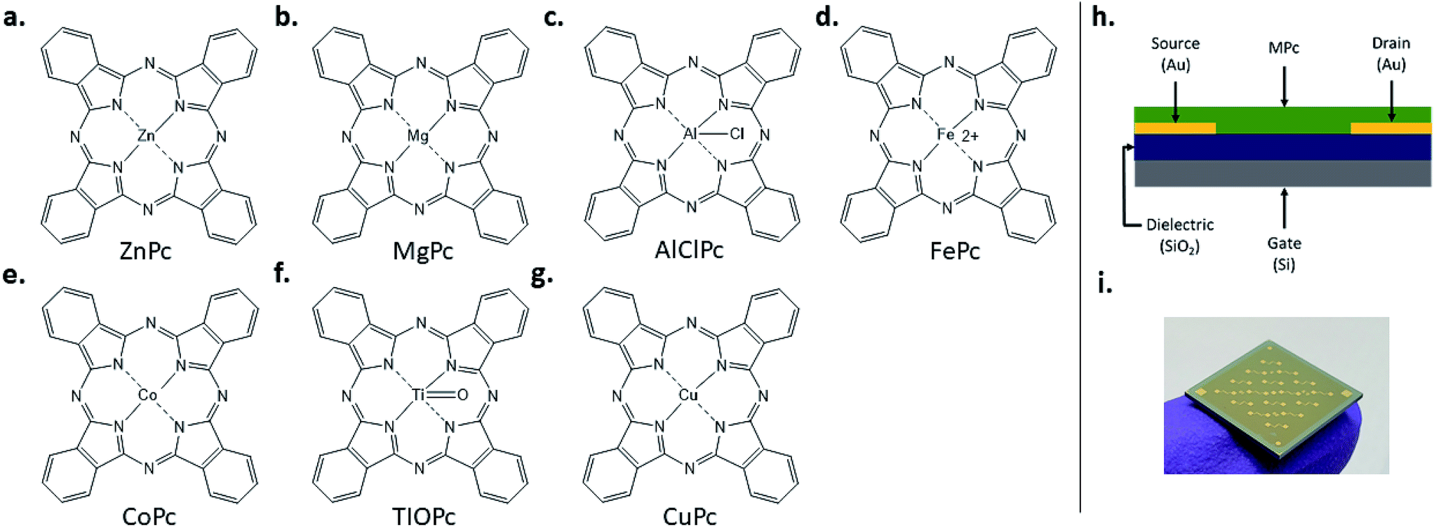 | ||
| Fig. 1 Chemical structure of (a) zinc phthalocyanine (ZnPc) (b) magnesium phthalocyanine (MgPc) (c) aluminium phthalocyanine chloride (AlClPc) (d) iron(II) phthalocyanine (FePc) (e) cobalt phthalocyanine (CoPc) (f) titanium oxide phthalocyanine (TiOPc) (g) copper phthalocyanine (CuPc). (h) Bottom gate bottom contact schematic of organic thin-film transistors fabricated and characterised and (i) is an image of a device chip including the MPc thin-film. | ||
Results and discussion
Baseline MPc OTFT device results
MPc-based BGBC OTFTs were fabricated by first forming a monolayer of trichloro(octyl)silane (OTS) on heavily doped silicon substrates with a thermally grown silicon dioxide dielectric followed by the thermal vacuum deposition of an MPc (ZnPc, MgPc, AlClPc, Fe(II)Pc, CoPc, or TiOPc) as the semiconducting layer. Electrical performance characteristics such as μH, VT and on/off current ratio (Ion/off) for each MPc- based OTFT in air and vacuum (P < 0.1 Pa) at 25 °C, are summarized in Table 1.| Materiala | Air | Vacuum | ||||
|---|---|---|---|---|---|---|
| μAvgb (cm2 V−1 s−1) | VT, Avgb (V) | Ion/off, Avgb | μAvgb (cm2 V−1 s−1) | VT, Avgb (V) | Ion/off, Avgb | |
| a ZnPc, MgPc, AlClPc, Fe(II)Pc, CoPc, or TiOPc. Devices were characterized at 25 °C in air or vacuum (P < 0.1 Pa). Data for CuPc devices was taken from a previous publication by our group,24 where the devices were fabricated and characterised under identical conditions.b μAvg = saturation-region mean field-effect mobility. VT, Avg = mean threshold voltage. Ion/off, Avg, mean on/off current.c MgPc and Fe(II)Pc were not found to be air stable in this device configuration. Three replicates were fabricated on three different days and did not exhibit transistor characteristics in air. | ||||||
| CoPc | 0.0031 | 1.4 | 103 | 0.003 | −32.7 | 103 |
| AlClPc | 0.04 | 2.0 | 104 | 0.001 | −13.6 | 104 |
| TiOPc | 0.062 | −15.4 | 104 | 0.011 | −23.4 | 104 |
| ZnPc | 0.02 | 10.5 | 103 | 0.015 | −19.7 | 103 |
| Fe(II)Pc | —c | —c | —c | 0.0056 | −13.5 | 103 |
| MgPc | —c | —c | —c | 0.0006 | 1.2 | 102 |
| CuPc24 | 0.024 | −5.7 | 104 | 0.014 | −13.4 | 103 |
The values in Table 1 show reasonable concurrence with the values in literature for MPc-based OTFTs fabricated with OTS, although some μH are one or two orders of magnitude lower (TiOPc) or higher (Fe(II)Pc) than the highest records reported.12 Improved electrical performance can be obtained by optimizing processing conditions such as lowering deposition rate, increasing substrate temperature, or using a different interfacial layer (e.g. para-sexiphenyl).25–28 While the Fe(II)Pc and MgPc devices were not found to be air stable (Table 1), there is at least one report of air stable MgPc OTFTs in top contact bottom gate (TCBG) configuration with an ITO gate electrode and parylene-C dielectric.29 As all devices presented here were fabricated under the same conditions for ease of internal comparison, some variations with regards to literature devices fabricated differently is expected.
AlClPc OTFTs
Of the materials used in this study AlClPc is the least investigated, with only one report of OTFTs.30 Those devices were fabricated similarly to the ones presented here: at elevated substrate temperature (120 °C) and on OTS modified dielectrics.The AlClPc OTFTs were characterised in air and reached mobilities of 0.06 cm2 V−1 s−1. In addition, hexadecafluoro and hexadecachloro modified AlClPcs in OTFTs have also been reported, resulting in N-type behaviour with electron mobilities (μE) from 0.01 to 0.02 cm2 V−1 s−1.31 Fig. 2 displays a series of curves depicting the characteristics of AlClPc in BGBC OTFTs including transfer curves (Fig. 2a) and μH vs. VGS curves (Fig. 2b and c) for a characteristic device. In air, AlClPc OTFTs were found to have a μH of 0.004 cm2 V−1 s−1 compared to 0.001 cm2 V−1 s−1 in vacuum (Table 1). This mobility increase is typical, as it is generally accepted that the oxygen in air coordinates with surface MPc metal centres, acting as an electron acceptor/trap and increasing positive charge carrier density in the bulk film.32–34
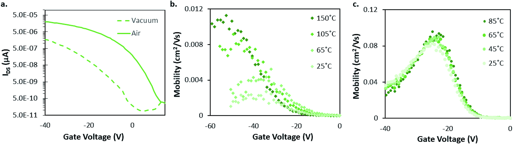 | ||
| Fig. 2 Characterization of AlClPc OTFTs. (a) Transfer curves for AlClPc BGBC devices deposited at T = 140 °C, and tested in air (VSD = −50 V), and vacuum, at T = 25 °C. VGS vs. μH curves at temperatures ranging from 25 °C to 150 °C in vacuum (b) and temperatures from 25 °C to 85 °C in air (c). | ||
Fig. 2b and c shows how μH changes with VGS at various temperatures under different environmental conditions. Experiments to collect this data were performed for all MPcs under varying environmental conditions and temperatures; Fig. S1–13 show this data and can be found in the ESI.† These curves give a more complete picture of how the MPc OTFTs respond to temperature/pressure changes than comparing single-values of μH and VT. Fig. 2b shows a consistent increase in the μH of AlClPc devices operated in vacuum with increasing temperature from 25 °C to 150 °C. Additionally, ΔVT < 0 is observed as an overall shift in these curves to the left towards more negative VGS with increasing temperature. In contrast, little ΔVT and minimal change in μH were observed with increasing temperature in air. Due to equipment heating limitations, we were unable to test at temperatures greater than 85 °C in air or 150 °C in vacuum.
MPc elevated temperature operation studies and material characterization
Similar to AlClPc, each BGBC MPc OTFT was characterised in the range of 25 °C to 85 °C in air, and in the range of 25 °C to 150 °C in vacuum. Fig. 3a illustrates average changes in VT in terms of relative change per °C between 25 °C and the maximum temperature value (85 °C in air, and 150 °C in vacuum), while Fig. 3b illustrates average changes in μH in terms of the percent change in μH from original baseline at 25 °C per °C between 25 °C and the maximum temperature (85 °C in air, and 150 °C in vacuum). It is important to note that the response to temperature is different between materials and different between vacuum and air. For example, under vacuum, AlClPc saw an increase in μH from 0.004 cm2 V−1 s−1 at 25 °C to 0.012 cm2 V−1 s−1 at 150 °C (Fig. 2), which corresponds to an increase in 4–5% change per °C (Fig. 3). In comparison, under vacuum, CoPc only saw an increase in μH from 0.0044 cm2 V−1 s−1 at 25 °C to 0.0075 cm2 V−1 s−1 at 150 °C (Fig. S1†), which corresponds to an increase in 0–2% change per °C (Fig. 3). In vacuum, similar but decreasing ΔVT > 0 shifts were seen in the descending order of CuPc, FePc, CoPc, and ZnPc. From MgPc, TiOPc, and AlClPc, increasing magnitude ΔVT < 0 were seen (Fig. 3a). In air, similar trends were seen but with ZnPc showing the highest ΔVT > 0 shift. In air, the divalent materials appear to have larger ΔVT > 0 shifts than the trivalent and tetravalent materials. AlClPc and TiOPc both have ΔVT < 0 in vacuum, although the change in TiOPc is not statistically significant. Negative ΔVT could be caused by increased trap density or the expulsion of dopant gases with increasing temperature. In air, all ΔμH > 0 except for AlClPc, with greater magnitude percentage changes per °C seen for the divalent metal inclusion (CuPc, ZnPc, CoPc) and small changes seen for the trivalent and tetravalent metal inclusion (AlClPc, TiOPc). The percentage ΔμH that is seen for the AlClPc is near zero when considering the standard deviation. In vacuum, a negative ΔμH across the temperature range is seen for TiOPc only, the rest remaining positive. Negative ΔμH in response to temperature increase is unexpected as μH is often accepted to be thermally activated in organic semiconductors.22,35 These results as a whole demonstrate that the nature of the metal inclusion in the MPc plays a significant role on the resulting OTFTs performance, with apparently larger performance differences between valency groups, than between MPcs of identical valency.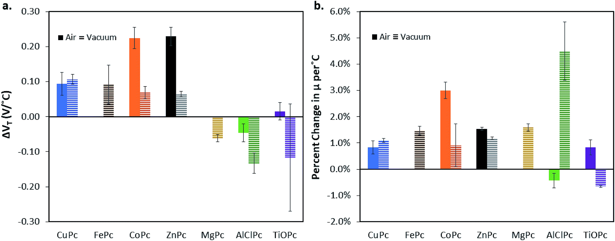 | ||
| Fig. 3 (a) Change in threshold voltage per degree celsius, (VT/°C) within the characterised temperature range (25 °C to 85 °C for air and 25 °C to 150 °C for vacuum) for each phthalocyanine material characterised in BGBC OTFT under air (solid bars), and vacuum (horizontal line bars). (b) % change in hole mobility, μH, compared to baseline at 25 °C per °C. Materials that did not function in air have no corresponding data (FePc, and MgPc). CuPc data shown is reproduced from previously published work for comparison.24 | ||
One important consideration when investigating BGBC OTFT responses to various stimuli is the thickness of the semiconductor layer. It's been reported that as the active layer thickness increases, degradation due to the bias stress effect also increases,36 but also that long term environmental stability increases with thickness for inkjet printed active layers.37 Fig. 4 shows these changes in both ΔVT and μH for CuPc devices in vacuum and in air. It was found that increasing active layer thickness resulted in reduced response magnitude to temperature changes in air over the tested temperature range.
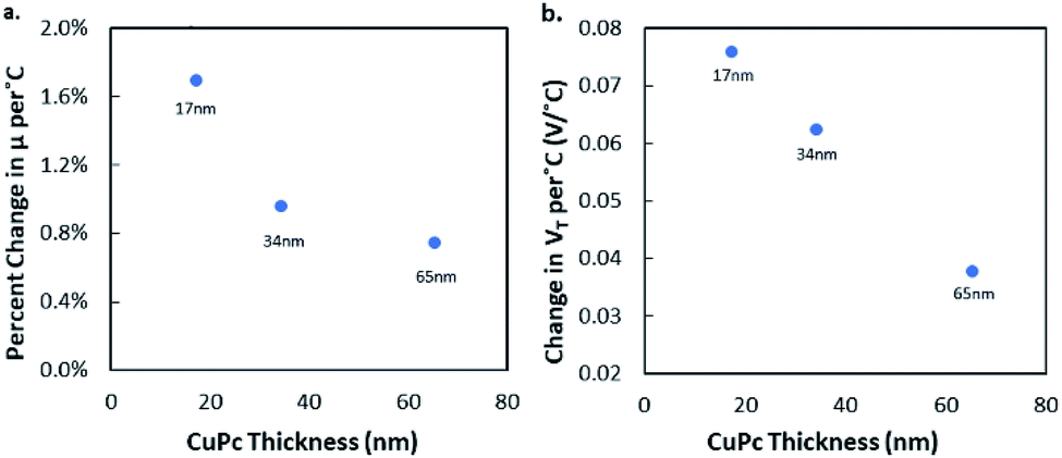 | ||
| Fig. 4 Effect of CuPc thickness on BGBC OTFTs performance as a function of temperature (between 25 °C and 85 °C for air and 20 °C to 150 °C for vacuum). (a) % change in hole mobility, μH compared to baseline at 25 °C per °C and (b) the change in threshold voltage VT per °C. | ||
To further investigate material differences, film morphology of the various MPc thin-films were characterised by atomic force microscopy (AFM) and can be found in Fig. 5. These images were taken from the same MPc thin-films used for devices discussed in the previous section. It would appear that valency of the metal inclusion leads to different solid-state packings resulting in different film morphologies as seen in Fig. 5. The divalent materials: CoPc, FePc, ZnPc, MgPc, and CuPc, all have similar grain structures and surface roughness values (Fig. 5h) with some slight variation in grain size. AlClPc, and TiOPc have distinct but similar film morphologies with the largest grain structures, and surface roughness values of 5.09 nm and 4.18 nm respectively. These larger grain sizes and higher surface roughness values could partly explain the lower changes in μH and VT in air seen by these two materials. It has been reported that larger surface roughness does play a role in how much water and oxygen will adsorb/coordinate at the surface.32 These platelets (Fig. 5b and e) would appear to have much lower surface area to volume ratios compared to the worm-like morphology of the divalent MPc films, which could contribute to a smaller susceptibility to ambient environment traps by reducing the access of ambient gasses to the overall volume. Little correlation between film properties and electrical response under vacuum is seen. This is reasonable as in air it is expected that the gases present will interact differently with different morphologies, while in vacuum no such gases are present, and the effects that are seen would be expected to be due solely to material differences. These remarkably different morphologies also suggest a different growth mode for the thin films of these MPc compounds, indicating that processing conditions could also play a role in device stability.
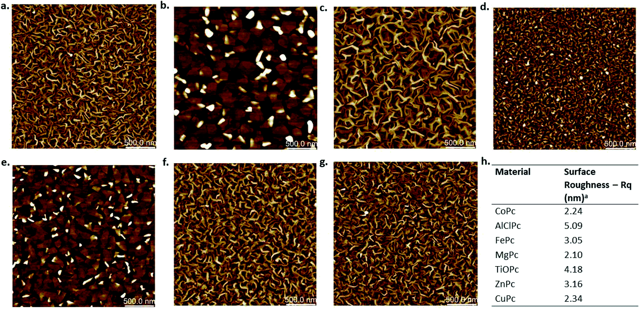 | ||
| Fig. 5 AFM images (2.5 μm × 2.5 μm) of (a) CoPc (b) AlClPc (c) FePc (d) MgPc (e) TiOPc (f) ZnPc (g) CuPc deposited on heated silicon substrates (T = 140 °C) under vacuum (h) surface roughness values (nm) for each film. | ||
Fig. 6 depicts the degradation temperature (TD) of each material determined by thermal gravimetric analysis (TGA) performed in either an air or nitrogen environment. The materials are ordered in terms of highest air stability by highest TD in air (from left to right). It can be seen that the air stable materials (as determined in the previous section through incorporation into OTFTs) have greater air TD values, while the non-functioning materials in air (MgPc, FePc) have the lowest air TD values. It is commonly understood that as oxidation occurs, VT will shift positively as more and more holes are generated in the bulk film, thus requiring higher positive VGS to stop conduction.38 Therefore it is plausible that materials that have lower TD in air are also more susceptible to oxidation effects, with the least stable oxidizing in air beyond the point of function. Overall, these correlations show that TGA could be a useful tool for screening materials for air stability, although further investigation is necessary to confirm these results across a large range of materials.
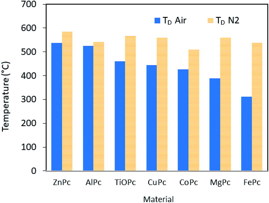 | ||
| Fig. 6 TD of MPcs in air (blue) or nitrogen (yellow horizontal lines). These temperatures were found from 5% mass degradation during TGA. | ||
Fig. 7 depicts how ISD varies with temperature at fixed VGS and VSD for MgPc and FePc devices. These experiments were done to illustrate the time dependent temperature response of the OTFTs to temperature change. Similar curves have been used to display sensor responses to injected analytes in the gas phase39 and liquid phase.40 These results illustrate response times, and show cumulative change that is otherwise not measured in typical transfer and output curves. The temperature response over time for both MgPc (Fig. 7a) and FePc (Fig. 7b) is quite similar. Both materials respond almost instantaneously, and drastically, to temperature change. This is seen by the essentially parallel current and temperature curves when temperature is increasing. These results show evidence for the possibility of constant temperature monitoring via OTFT-based temperature sensors. Further investigation is warranted to explore current responses under varying conditions, and with different materials.
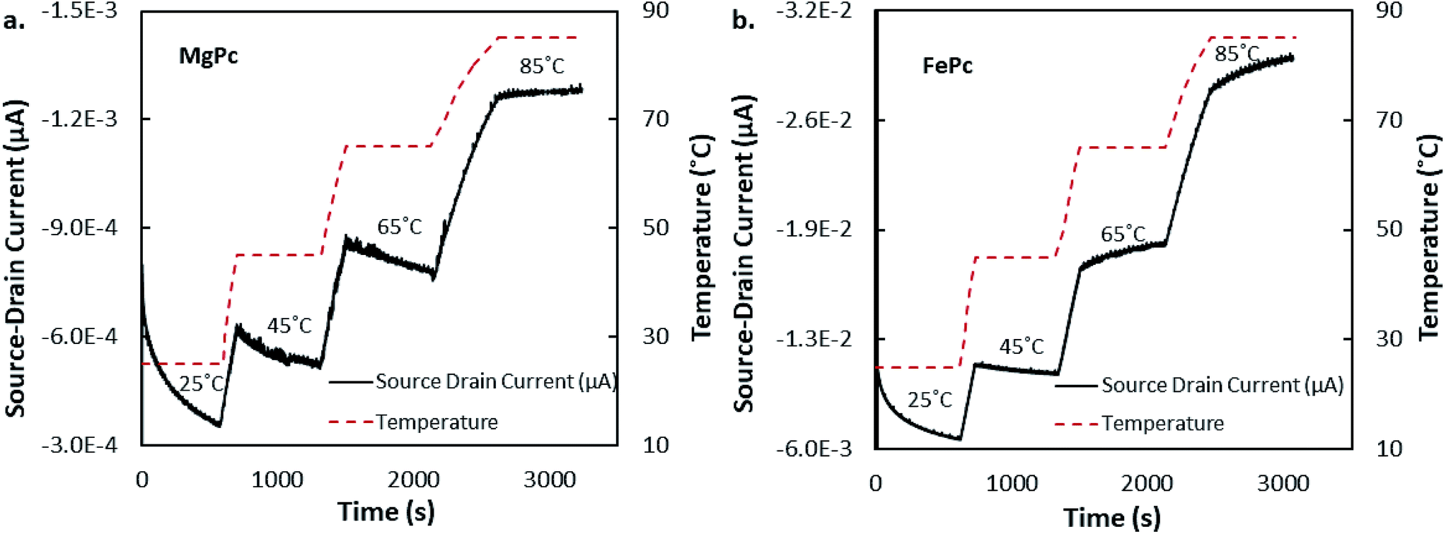 | ||
| Fig. 7 Current response to temperature changes at constant voltages, with VSD = −50 V. (a) MgPc BCBG devices, VGS = −30 V and (b) FePc devices, VGS = −60 V, were held at a constant bias while the ISD was measured. The devices began testing at T = 25 °C and the temperature was increased at regular timepoints up to 85 °C in vacuum. | ||
Experimental
Materials
Copper phthalocyanine (CuPc, 90%, #P1005), and aluminum phthalocyanine chloride (AlClPc, 98%, #C1167) were obtained from TCI Chemicals. Cobalt(II) phthalocyanine (CoPc, >99%, #LT-D2001), titanium oxide phthalocyanine (TiOPc, >99%, #LT-E206), zinc phthalocyanine (ZnPc, >99%, #LT-S906), iron(II) phthalocyanine (FePc, >99%, #LT-D2009), and magnesium(II) phthalocyanine (MgPc, >99%, #LT-D2006) were obtained from Luminescence Technology Corp. CuPc and AlClPc were purified once by train sublimation before use. All chemicals were used as received unless otherwise specified.Preparation of devices
Heavily N-doped silicon substrates with a 230 nm SiO2 dielectric and prefabricated gold source–drain electrodes from Fraunhofer IPMS (W = 2000 μm, L = 20 μm) were washed with acetone and dried with nitrogen. They were then treated with oxygen plasma for 15 minutes to clean and hydrolyze the surface. Substrates were then rinsed with water and isopropanol, before a 1 hour surface treatment in 1% v/v octyltrichlorosilane (OTS) in toluene at 70 °C. Silane-treated substrates were washed with toluene and isopropanol and dried for 1 hour at 70 °C under vacuum. All materials were deposited using physical vapour deposition in an Angstrom EvoVac thermal evaporator with a target thickness of 300 Å and a rate of 0.3 Å s−1 at 140 °C. Heated substrates were allowed to cool to room temperature before being removed from the vacuum chamber, usually overnight.OTFT testing & electrical characterization
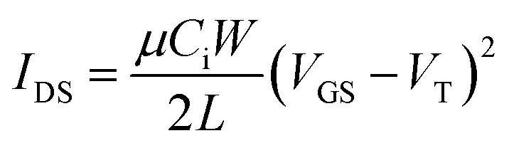
Contact with the source–drain electrodes was made with BeCu alloy probe tips. Output curves were obtained by fixing the gate voltage (VGS) at discrete values and sweeping the source–drain voltage (VSD). Electrical measurements were performed using a custom electrical probe station with a chamber allowing for controlled atmosphere, oesProbe A10000-P290 (Element Instrumentation Inc. & Kreus Design Inc.) with a Keithley 2614B to control source–drain voltage (VDS), gate voltage (VGS), and measure source–drain current (IDS). VDS was held constant while VGS was varied to obtain measurements of IDS. From these measurements, saturation region field-effect mobility, on/off current ratio, and threshold voltage were determined. The general expression relating current to field-effect mobility and gate voltage in the saturation mode is given in eqn (1):
 | (1) |
 curve.
 | (2) |
Finally, the on/off ratio is determined by eqn (3):
 | (3) |
Varying temperature experiments
Temperature variation experiments were performed by heating the devices on a conductive metal surface to a starting temperature of 25 °C. Once the target temperature was reached, the device was left for 10 minutes to ensure thermal equilibrium was achieved. After this, electrical characterization was performed. Each device was then sequentially heated to temperatures of 45 °C, 65 °C, and 85 °C in air, or 65 °C, 105 °C, and 150 °C in vacuum, waiting 10 minutes at each temperature before electrical characterization. Constant voltage temperature response experiments (Fig. 7) were carried out by holding the VDS and VGS constant to obtain IDS measurements. For these experiments, electrical characterization was continuously performed in vacuum on a device while increasing the temperature to 25 °C, 45 °C, 65 °C, and 85 °C. Each temperature was held for 10 minutes.AFM
AFM measurements were collected using a Bruker Dimension Icon AFM with ScanAsyst-Air tips. All images were collected in tapping mode at a scan rate of 1 Hz, an image size of 2.5 × 2.5 μm, and with a resolution of 512 pixels. To process and edit the images, NanoScope Analysis v.1.8 was used.Conclusions
BGBC OTFT devices were fabricated with seven different MPcs as the semiconducting layer and were characterised under varying environmental conditions. The divalent MPcs showed consistently greater changes in threshold voltage and mobility in response to temperature change. AlClPc and TiOPc, on the other hand, show generally on average smaller changes in performance with temperature. We also demonstrated that the thickness in CuPc layer (and likely other semiconductor layer) does play an important role in the rate of change the BGBC OTFT device experiences with temperature and environment. AFM demonstrated drastically different film morphologies with different grain size for the trivalent and tetravalent MPcs compared to the divalent MPcs, suggesting that the OTFT device stability is likely correlated to film morphology. Thermogravimetric analysis (TGA) in air and under N2 demonstrate that different materials have different thermal stability while giving insight into their susceptibility to oxidation. The relatively low degradation temperature in air relative to in nitrogen for FePc and MgPc could explain why the resulting OTFTs are not air stable. Constant bias–current curves demonstrated the real-time response of the OTFTs to temperature changes. Stability is important in both OTFT and other organic electronic applications such as organic photovoltaic (OPV) operation, and therefore is relevant for material selection. This study suggests that trivalent and tetravalent MPcs are favourable for OTFTs as they display more stability to temperature in ambient conditions, while the divalent MPcs appear to be more affected by variable temperature operation which could be useful in temperature sensing applications.Conflicts of interest
There are no conflicts of interests to declare.Acknowledgements
The authors are very grateful for financial support from the NSERC DG, RTI and SPG-P to B. L. and PGS-D to N. T. B. and B. M. O. A. M. is grateful to OGS for support.Notes and references
- O. A. Melville, T. M. Grant and B. H. Lessard, Silicon phthalocyanines as N-type semiconductors in organic thin film transistors, J. Mater. Chem. C, 2018, 6, 5482–5488 RSC.
- M.-T. Dang, et al., Bis(tri-n-alkylsilyl oxide) silicon phthalocyanines: a start to establishing a structure property relationship as both ternary additives and non-fullerene electron acceptors in bulk heterojunction organic photovoltaic devices, J. Mater. Chem. A, 2017, 5, 12168–12182 RSC.
- J. Blochwitz, M. Pfeiffer, T. Fritz and K. Leo, Low voltage organic light emitting diodes featuring doped phthalocyanine as hole transport material, Appl. Phys. Lett., 1998, 73, 729 CrossRef CAS.
- M. Gsänger, D. Bialas, L. Huang, M. Stolte and F. Würthner, Organic Semiconductors based on Dyes and Color Pigments, Adv. Mater., 2016, 28, 3615–3645 CrossRef.
- Y. Zhang and J. F. Lovell, Recent applications of phthalocyanines and naphthalocyanines for imaging and therapy, Wiley Interdiscip. Rev.: Nanomed. Nanobiotechnol., 2017, 9, e1420 Search PubMed.
- A. B. Sorokin, Phthalocyanine Metal Complexes in Catalysis, Chem. Rev., 2013, 113, 8152–8191 CrossRef CAS.
- L. Li, et al., An Ultra Closely π-Stacked Organic Semiconductor for High Performance Field-Effect Transistors, Adv. Mater., 2007, 19, 2613–2617 CrossRef CAS.
- O. A. Melville, T. M. Grant, B. Mirka, N. Boileau and B. H. Lessard, Ambipolarity and Air Stability of Silicon Phthalocyanine Organic Thin-Film Transistors, Adv. Electron. Mater., 2019, 1900087 CrossRef.
- L. Li, et al., Organic thin-film transistors of phthalocyanines, Pure Appl. Chem., 2008, 80, 2231–2240 CAS.
- C. G. Claessens, U. Hahn and T. Torres, Phthalocyanines: from outstanding electronic properties to emerging applications, Chem. Rec., 2008, 8, 75–97 CrossRef CAS PubMed.
- G. de la Torre, C. G. Claessens and T. Torres, Phthalocyanines: old dyes, new materials. Putting color in nanotechnology, Chem. Commun., 2007, 2000–2015 RSC.
- O. A. Melville, B. H. Lessard and T. P. Bender, Phthalocyanine-Based Organic Thin-Film Transistors: A Review of Recent Advances, ACS Appl. Mater. Interfaces, 2015, 7, 13105–13118 CrossRef CAS.
- F. I. Bohrer, et al., Comparative Gas Sensing in Cobalt, Nickel, Copper, Zinc, and Metal-Free Phthalocyanine Chemiresistors, J. Am. Chem. Soc., 2009, 131, 478–485 CrossRef CAS.
- G. Williams, S. Sutty, R. Klenkler and H. Aziz, Renewed interest in metal phthalocyanine donors for small molecule organic solar cells, Sol. Energy Mater. Sol. Cells, 2014, 124, 217–226 CrossRef CAS.
- A. P. Yuen, et al., Photovoltaic properties of M-phthalocyanine/fullerene organic solar cells, Sol. Energy, 2012, 86, 1683–1688 CrossRef CAS.
- R. F. Bailey-Salzman, B. P. Rand and S. R. Forrest, Near-infrared sensitive small molecule organic photovoltaic cells based on chloroaluminum phthalocyanine, Appl. Phys. Lett., 2007, 91, 013508 CrossRef.
- M. Brumbach, D. Placencia and N. R. Armstrong, Titanyl Phthalocyanine/C60 Heterojunctions: Band-Edge Offsets and Photovoltaic Device Performance, J. Phys. Chem. C, 2008, 112, 3142–3151 CrossRef CAS.
- X. Ren, P. K. L. Chan, J. Lu, B. Huang and D. C. W. Leung, High Dynamic Range Organic Temperature Sensor, Adv. Mater., 2013, 25, 1291–1295 CrossRef CAS.
- K. Kuribara, et al., Organic transistors with high thermal stability for medical applications, Nat. Commun., 2012, 3, 723 CrossRef.
- S. Jung, T. Ji and V. K. Varadan, Point-of-care temperature and respiration monitoring sensors for smart fabric applications, Smart Mater. Struct., 2006, 15, 1872–1876 CrossRef.
- D. Kawakami, Y. Yasutake, H. Nishizawa and Y. Majima, Bias Stress Induced Threshold Voltage Shift in Pentacene Thin-Film Transistors, Jpn. J. Appl. Phys., 2006, 45, L1127–L1129 CrossRef CAS.
- H.-K. Chen, P.-T. Liu, T.-C. Chang and S.-L. Shy, Variable Temperature Measurement on Operating Pentacene-Based OTFT, MRS Proceedings, 2008, 1091, 1091-AA07–91 CrossRef.
- S. Brixi, O. A. Melville, N. T. Boileau and B. H. Lessard, The influence of air and temperature on the performance of PBDB-T and P3HT in organic thin film transistors, J. Mater. Chem. C, 2018, 6, 11972–11979 RSC.
- N. T. Boileau, O. A. Melville, B. Mirka, R. Cranston and B. H. Lessard, P and N type copper phthalocyanines as effective semiconductors in organic thin-film transistor based DNA biosensors at elevated temperatures, RSC Adv., 2019, 9, 2133–2142 RSC.
- X. Shao, et al., Single component p-, ambipolar and n-type OTFTs based on fluorinated copper phthalocyanines, Dyes Pigm., 2016, 132, 378–386 CrossRef CAS.
- L. Huang, et al., Tin (IV) phthalocyanine oxide: an air-stable semiconductor with high electron mobility, Appl. Phys. Lett., 2008, 92, 143303 CrossRef.
- H. Wang, F. Zhu, J. Yang, Y. Geng and D. Yan, Weak Epitaxy Growth Affording High-Mobility Thin Films of Disk-Like Organic Semiconductors, Adv. Mater., 2007, 19, 2168–2171 CrossRef CAS.
- W. Gu, et al., Preparing highly ordered copper phthalocyanine thin-film by controlling the thickness of the modified layer and its application in organic transistors, Solid-State Electron., 2013, 89, 101–104 CrossRef CAS.
- K. R. Rajesh and C. S. Menon, Polymeric gated organic field effect transistor using magnesium phthalocyanine, Proc. SPIE, 2014, 9185, 918515 CrossRef.
- L. Li, W. Hu, H. Fuchs and L. Chi, Controlling Molecular Packing for Charge Transport in Organic Thin Films, Adv. Energy Mater., 2011, 1, 188–193 CrossRef CAS.
- D. Yan, D. Song and B. Y. Feng Zhu, Use of axial substituted phthalocyanine compound for preparing organic thin-film transistor, 2008 Search PubMed.
- H. R. Kerp, K. T. Westerduin, A. T. van Veen and E. E. van Faassen, Quantification and effects of molecular oxygen and water in zinc phthalocyanine layers, J. Mater. Res., 2001, 16, 503–511 CrossRef CAS.
- H. Yasunaga, K. Kojima, H. Yohda and K. Takeya, Effect of Oxygen on Electrical Properties of Lead Phthalocyanine, J. Phys. Soc. Jpn., 1974, 37, 1024–1030 CrossRef CAS.
- H. Laurs and G. Heiland, Electrical and optical properties of phthalocyanine films, Thin Solid Films, 1987, 149, 129–142 CrossRef CAS.
- R. J. Chesterfield, et al., Variable temperature film and contact resistance measurements on operating n-channel organic thin film transistors, J. Appl. Phys., 2004, 95, 6396–6405 CrossRef CAS.
- J. B. Chang and V. Subramanian, Effect of active layer thickness on bias stress effect in pentacene thin-film transistors, Appl. Phys. Lett., 2006, 88, 233513 CrossRef.
- M. H. Choi, et al., Effect of active layer thickness on environmental stability of printed thin-film transistor, Org. Electron., 2009, 10, 421–425 CrossRef CAS.
- H. Sirringhaus, Reliability of Organic Field-Effect Transistors, Adv. Mater., 2009, 21, 3859–3873 CrossRef CAS.
- J. W. Jeong, et al., The response characteristics of a gas sensor based on poly-3-hexylithiophene thin-film transistors, Sens. Actuators, B, 2010, 146, 40–45 CrossRef CAS.
- H. U. Khan, M. E. Roberts, O. Johnson, W. Knoll and Z. Bao, The effect of pH and DNA concentration on organic thin-film transistor biosensors, Org. Electron., 2012, 13, 519–524 CrossRef CAS.
Footnote |
| † Electronic supplementary information (ESI) available. See DOI: 10.1039/c9ra03648b |
| This journal is © The Royal Society of Chemistry 2019 |