
 Open Access Article
 This Open Access Article is licensed under a Creative Commons Attribution-Non Commercial 3.0 Unported Licence
Electronic and magnetic properties of a black phosphorene/Tl2S heterostructure with transition metal atom intercalation: a first-principles study†
Yusheng Wang *ac,
Xiaoyan Songa,
Nahong Songbc,
Tianjie Zhanga,
Xiaohui Yanga,
Weifen Jianga and
Jianjun Wangd
*ac,
Xiaoyan Songa,
Nahong Songbc,
Tianjie Zhanga,
Xiaohui Yanga,
Weifen Jianga and
Jianjun Wangd
aCollege of Physics and Electronics, North China University of Water Resources and Electric Power, Zhengzhou, Henan 450046, China. E-mail: wangyusheng@ncwu.edu.cn
bCollege of Computer and Information Engineering, Henan University of Economics and Law, Zhengzhou, Henan 450000, China
cInternational Joint Research Laboratory for Quantum Functional Materials of Henan, School of Physics and Engineering, Zhengzhou University, Zhengzhou 450001, China
dCollege of Science, Zhongyuan University of Technology, Zhengzhou 450007, China
First published on 20th June 2019
Abstract
Using density functional theory calculations, the structural, electronic and magnetic properties of a black phosphorene/Tl2S heterostructure (BP/Tl2S) and the BP/Tl2S intercalated with transition metal atoms (TMs) have been detailed investigated. It is demonstrated that the BP/Tl2S is a type-I van der Waals (vdW) heterostructure with an indirect band gap of approximately 0.79 eV. The BP/Tl2S experiences a transition from type-I to type-II when various strains are applied. In addition, the BP/Tl2S intercalated with TMs (TM-BP/Tl2S) exhibits various kinds of meaningful electronic and magnetic properties. Several TM-BP/Tl2S systems are still non-magnetic ground states and six TM-BP/Tl2S (Ti-, V-, Cr-, Mn-, Fe-, Tc-) systems are ferromagnetic. Interestingly, three TM-BP/Tl2S (V-, Cr-, Mn-) systems display half-metallic character. The Fe-BP/Tl2S and Tc-BP/Tl2S are dilute magnetic semiconductors (DMSs), while TM-BP/Tl2S (Mo-, Pd-, Ni-) systems are semiconductors. The other TM-BP/Tl2S systems become metals. These results may open a new avenue for application of the BP/Tl2S in future spintronic and electronic devices.
1. Introduction
At present, genuine interest is brewing in the scientific community in heterostructures that could possess the advantages of two or more two-dimensional (2D) materials and expand the functions of 2D materials. A great deal of effort has been devoted to heterostructures experimentally and theoretically, such as graphene/phosphorene,1,2 GeSe/phosphorene,3 phosphorene/MoS2,4–6 MoS2/BN,7–10 SiC/MoS2,11 graphene/bilayer-GaSe,12 and so on.10,13 Phosphorene, an emerging 2D material with an obvious bandgap, may be superior to the graphene for device applications in many ways and stimulates lots of theoretical research.14–17 Of prominence, scientific progress in phosphorene-based heterostructures has been overwhelming in the fields of optoelectronics and nanoelectronics.1,4–6,18–21 GeSe/phosphorene has an intrinsic type-II band alignment and shows great potential to act as a good candidate for applications in optoelectronics due to spontaneous electron–hole charge separation.3In recent years, thallium sulfide (Tl2S) with semiconductor properties, a representative of metal-shrouded 2D materials, has been paid more attention than other metal-shrouded 2D materials.22–25 Moreover, the Tl2S monolayer adopting an anti-CdCl2 structure is theoretically verified to be thermally and dynamically stable.26 Most importantly, the distinctive metal-shrouded structure makes monolayer Tl2S own many intriguing properties such as strong light absorption and ideal photo-electricity transduction,27 implying Tl2S could be an excellent candidate for a wide range of applications in electronic and optoelectronic devices. It is interesting to explore the vdW heterostructure composed of BP and monolayer Tl2S. Therefore, in this paper, we investigate the structural and electronic properties of BP/Tl2S vdW heterostructures. Strain engineering is a valid way to modify the electronic and magnetic properties of 2D materials. Hence, it is significant to explore the electronic structure of the BP/Tl2S under strains by first-principles calculations. The transitions from type-I to type-II band alignment and from semiconductor to metal are observed under uniaxial and biaxial strain.
Previous work has reported that the interlayer interaction can be effectively changed by intercalating impurity atoms between layers, leading to the electronic and magnetic properties varying accordingly. It was reported that the transition from semiconductor to metal was observed in KxMoS2 with increasing potassium intercalation.28 Shahid Sattar et al. demonstrated that intercalating NH3 molecules between silicene and monolayer PtSe2 could weak the interlayer interaction.29 Moreover, Yongji Gong et al. not only shown that the intercalation method was workable, but also found that the TM was advantageous over alkali metals, rare earth metals when they were intercalated crystals.30 Lately, a new study found that the bilayer WSe2 intercalated with TMs (Cr, Mn, Fe, Co, Ni) exhibited a half-metallic character with a 100% spin polarization at the Fermi level due to the strong hybridization between the TMs and the parent W and Se atoms.31 These inspire us to study the structural, electronic and magnetic properties of the BP/Tl2S intercalated with all kinds of TMs (3d and 4d TM atoms). The results indicated that the half-metal and DMS character were induced in the BP/Tl2S by intercalating TMs. These findings may provide a new route for looking for the suitable candidate materials for spintronic devices, owing to the half-metallic and DMS properties of the BP/Tl2S intercalated with TMs (V, Cr, Mn, Fe, Tc).
2. Computational details
The present calculations are performed by employing spin-polarized density functional theory as implemented in the Vienna Ab initio Simulation Package (VASP).32–34 We adopt the optB88-vdW35,36 density functional to describe the long range vdW interaction because it can give a reasonable description for various layered compounds systems such as tellurene/MoS2 heterostructure,37 chromium trihalide38 and so on. The exchange and correlation functional is treated using the generalized gradient approximation (GGA) in the Perdew–Burke–Ernzerhof (PBE).39 A kinetic energy cutoff 500 eV is used in all simulations. An enough large vacuum layer thickness of 20 Å is added to each heterostructure to avoid spurious interaction between periodic images in the out-of-plane direction. The first Brillouin zone is sampled with a 7 × 5 × 1 Monkhorst–Pack grid for the relaxation of BP, Tl2S, BP/Tl2S and the TM-BP/Tl2S, respectively. All the structures are fully relaxed with an energy and a force tolerance of 10−5 eV and 0.01 eV Å−1 respectively.3. Results and discussion
3.1 BP/Tl2S
In view of the optimized structure, the optimized lattice constants of BP in our calculation are a = 3.297 Å and b = 4.615 Å, which are in good agreement with the previous results.40,41 Our optimized lattice constant for Tl2S is a1 = a2 = 4.18 Å, which also agrees with the cell parameters of the single crystal reported by the experiment.42 Using a lattice match model, the combination of a 2 × 2 periodicity of BP (a = 6.59 Å, b = 9.22 Å, containing 16 P atoms) and a Tl2S monolayer supercell (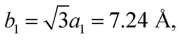 b2 = 2a2 = 8.37 Å, containing 4 S and 8 Tl atoms) is used for the simulation of the BP/Tl2S vdW heterostructure. In order to decrease the lattice mismatch between BP and Tl2S, the lattice constant is compressed or stretched to be a = 6.80 Å and b = 8.88 Å in the BP and Tl2S supercell, leading to a lattice mismatch of around 6.08%, 6.01% in both (x and y) directions. There are no significant changes of the electronic structure observed in BP and Tl2S because the sublattice symmetry is still maintained. Therefore, the BP/Tl2S is expected feasible in theory.
According to the geometry properties of the monolayer BP and Tl2S, for simplicity sake, only two representative configurations are taken into account, namely, A-stacking and B-stacking. The corresponding fully optimized top and side view of the BP/Tl2S are shown in Fig. 1(c) and (d). As for A-stacking, the half Tl atoms of the bottom layer of Tl2S marked by the red dashed circle are placed above the P atoms of the top layer of BP, whereas another half Tl atoms marked by the blue dashed circle are located above the puckered hexagon center of BP (see in Fig. 1(c)). For B-stacking, all the lower Tl atoms labeled by the yellow dashed circle are placed on top of bridge site (see Fig. 1(d)). In order to find essentially the most stable stacking manner, the binding energy (Eb) between the stacking layers in the BP/Tl2S is calculated as follows:
| Eb = [E(BP/Tl2S) − E(BP) − E(Tl2S)]/n | (1) |
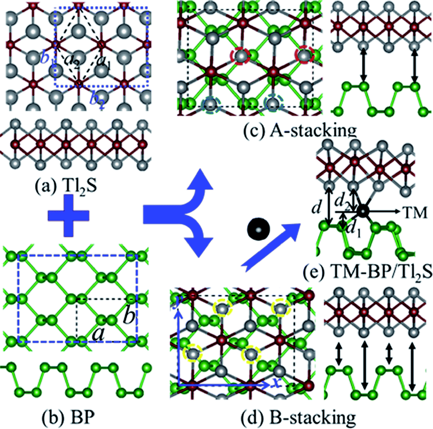 | ||
| Fig. 1 The top and side view of (a) Tl2S, (b) BP. (c) A-stacking of the BP/Tl2S, (d) B-stacking of the BP/Tl2S. (e) The BP/Tl2S heterostructure with TM atoms intercalated. The green, gray, wine red and black balls represent P, Tl, S and TM atoms, respectively. | ||
To further clarify the interaction between BP and Tl2S, the charge density difference Δρ(z) along the z direction is calculated by using the following equation:
| Δρ(z) = ρ(BP/Tl2S) − ρ(BP) − ρ(Tl2S) | (2) |
 | (3) |
The vivid differential charge density of BP/Tl2S is shown in the inset of Fig. 2(a). The yellow and blue colors indicate the charge accumulation and depletion of the BP/Tl2S. One can see clearly from Fig. 2(a) that BP donates electrons to the Tl2S layer, which leads to p-doping in BP layer. In addition, in order to explore its interlayer properties, the plane-averaged electrostatic potential along the perpendicular direction (z direction) of the BP/Tl2S is shown in Fig. 2(b). The striking characteristics is that there exists a large potential drop of ΔV across the BP/Tl2S interface 9.91 eV, which is much larger than the values of the GeSe/BP (5.94 eV),3 graphene/BP (6.42 eV),19 blue phosphorene/g-GaN (7.31 eV) and blue phosphorene/graphene (5.84 eV).43 Such a large potential drop implies that there exists a strong electrostatic field between BP and Tl2S, which is in favors of charge injection, leading to the better device performance if the BP/Tl2S is put into practical use.
 | ||
| Fig. 2 (a) The planar-averaged differential charge density of the BP/Tl2S heterostructure (Δρ(z)), and the amount of transferred charge along the z direction (ΔQ(z)). (b) The planar-averaged electrostatic potentials of the BP/Tl2S heterostructure. The inset in (a) shows charge density difference with an isovalue of 0.0025 e Å−3. The yellow and blue regions denote the gain and loss of electrons, respectively. | ||
It is also necessary to analyze the band structure of the BP/Tl2S, in order to comprehensively understand the properties of the BP/Tl2S. The separate BP monolayer and Tl2S are direct band gap semiconductors with the valence band maximum (VBM) and the conduction band minimum (CBM) at the Γ point (see Fig. 3(a) and (b)), the corresponding bandgaps are 0.894 eV and 1.37 eV, respectively, which are in agreement with the previous theoretical calculations.26 However, the BP/Tl2S becomes an indirect bandgap semiconductor with the VBM at the A point and CBM at the Γ point (see Fig. 3(c)). The bandgap of the BP/Tl2S is 0.79 eV. The partial charge densities of the BP/Tl2S for CBM and VBM are depicted in Fig. 3(d) and (e). It is clearly showed that the CBM is dominated by S atoms and the VBM comes mainly from S and Tl atoms. Hence, the type-I band alignment is obtained due to CBM and VBM being from the Tl2S in the BP/Tl2S, which is accord with the band structure of BP/Tl2S (Fig. 3(c)). In order to find out the effect of stacking type on the band structure, we also calculated the band structure of A stacking BP/Tl2S as shown in Fig. S4.† It can be found that the band structures of the two stacking types are almost the same. The band gaps are 0.796 eV and 0.794 eV for A-stacking and B-stacking, respectively. The tiny difference of band gap indicates that the stacking type of BP/Tl2S has little influence on the band structure of BP/Tl2S.
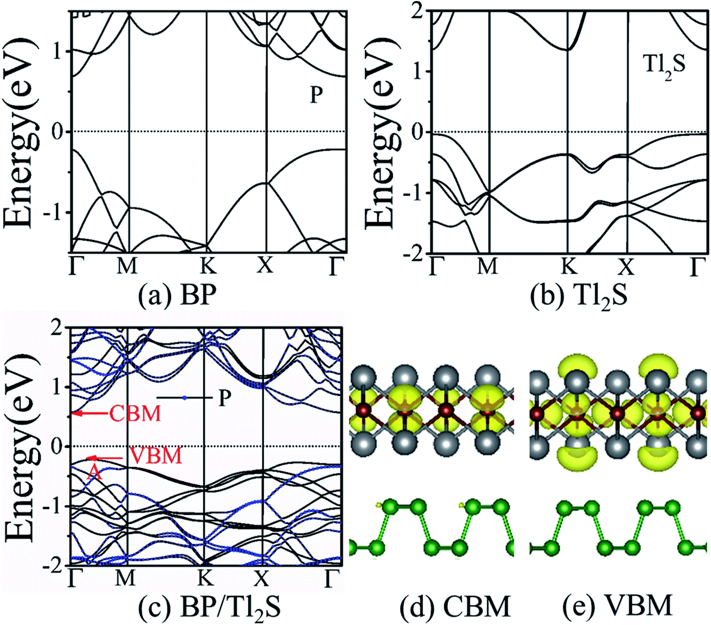 | ||
| Fig. 3 Band structures for (a) the monolayer BP, (b) the monolayer Tl2S, (c) the BP/Tl2S heterostructure. The band partial charge density of the BP/Tl2S heterostructure: (d) CBM, (e) VBM. The value of isosurfaces is 0.0025 e Å−3. | ||
To examine the effect of spin–orbital-coupling (SOC)44 on the band structure of BP/Tl2S, we calculated the band structure of the heterostructure by considering SOC effect (Fig. S2†). There is no obvious difference in the band structures of BP/Tl2S with and without SOC effect, suggesting that the SOC effect is negligible.
The carrier mobility of the heterostructure has a great effect on the performance of electronic devices.45 Therefore, according to the following formula, we calculate the effective mass of holes and electrons of BP/Tl2S
 | (4) |
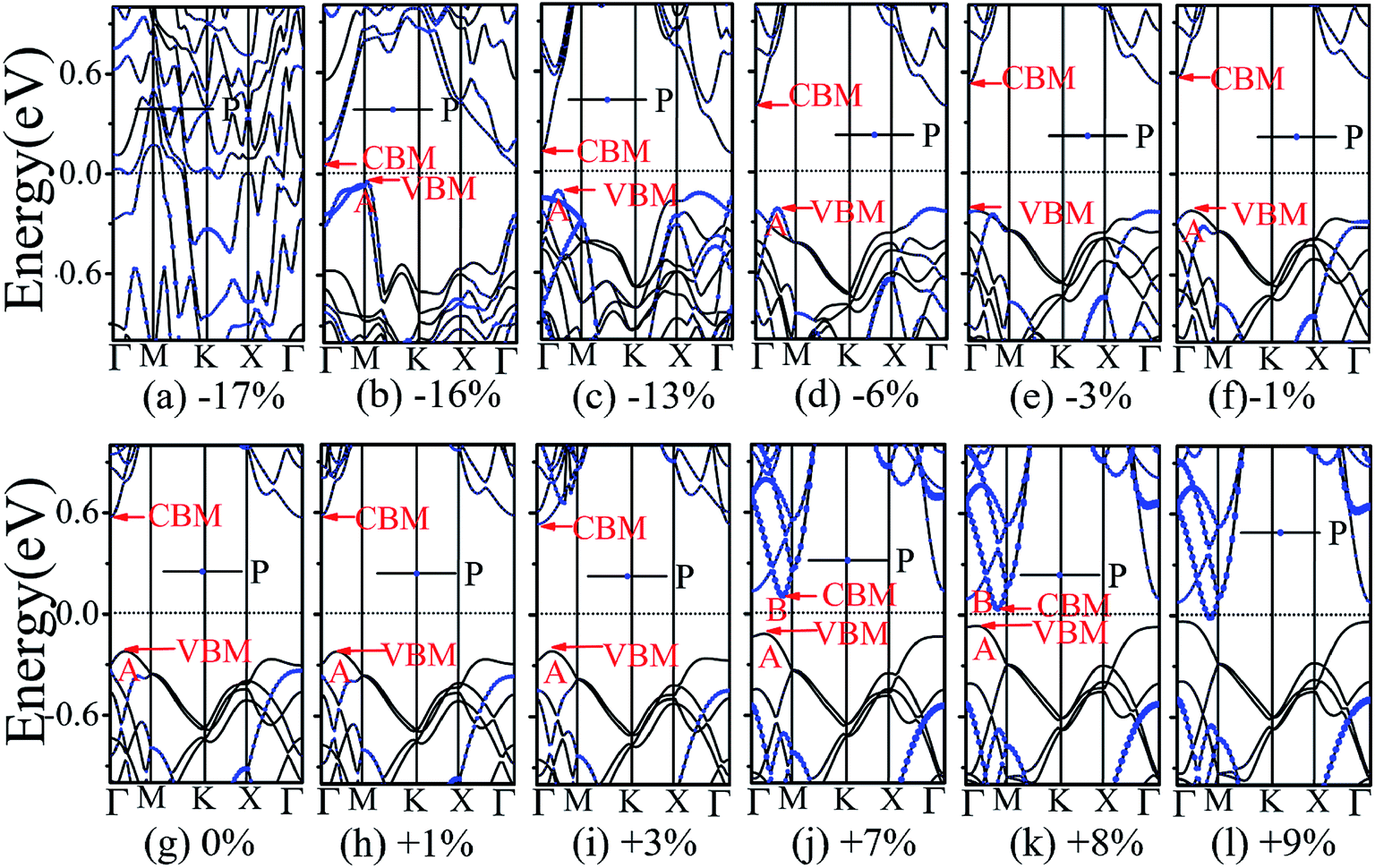
The application of strain has been proved to be a very effective approach to modulate the electronic properties of 2D materials. Very recently, Peng et al. revealed that the band structure of BP can be effectively tuned via the application of axial strain.48 Thus, we believe that a controllable band gap of the BP/Tl2S may also be obtained by this approach. By calculating the band gaps of BP/Tl2S at different values of axial strains, we find that the strain has a remarkable effect on the band structures (see Fig. 4). We can see the same characters that the band gap monotonically decreases with an increase of tensile and stress strain in the x and y direction and biaxial uniform strain. For the strain applied in the biaxial uniform situation, the gap sharply drops to 0 eV from the initial value of 0.79 eV at −6% and +7% (see Fig. 5(a) and (j)). For the strain applied in x direction, the band gap is sensitive to stress strain and decrease to zero at −8% (see Fig. 6(a)). However, the gap decreases tardily to 0.49 eV at +10% tensile strain. In order to see if the gap can reduce to zero with further increased tensile strain, we explore even larger strain up to +25% with a 1% increment. We find the band gap reaches a minimal value of 0.011 eV at +22% and then opens up again for larger strain (see Fig. 6). On the contrary, for the strain applied in y direction, the band gap is more sensitive to tensile strain than stress strain. The band gap becomes to zero at +9% (see Fig. 7(l)), while the band gap does not become zero until the stress strain increases to −17% (see Fig. 7(f)).
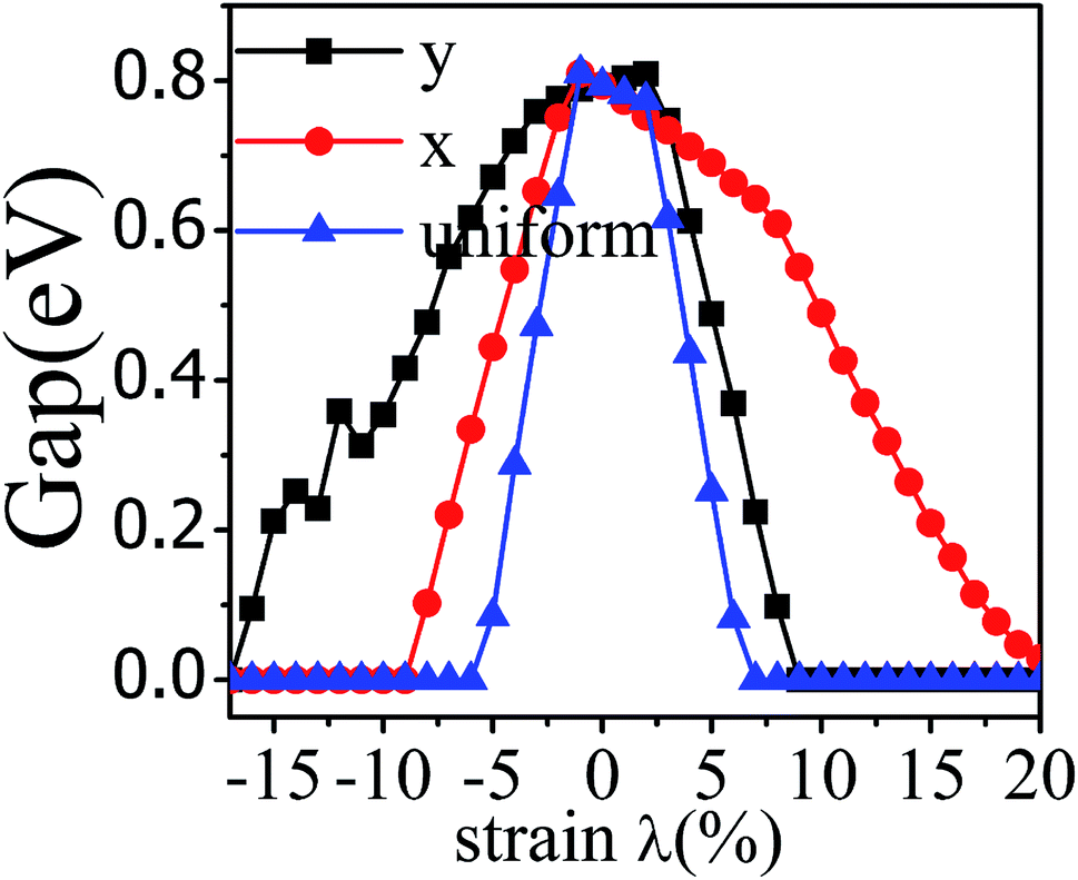 | ||
| Fig. 4 The band gap of the BP/Tl2S as a function of strain (λ%) applied in x, y direction and biaxial uniform strain. | ||
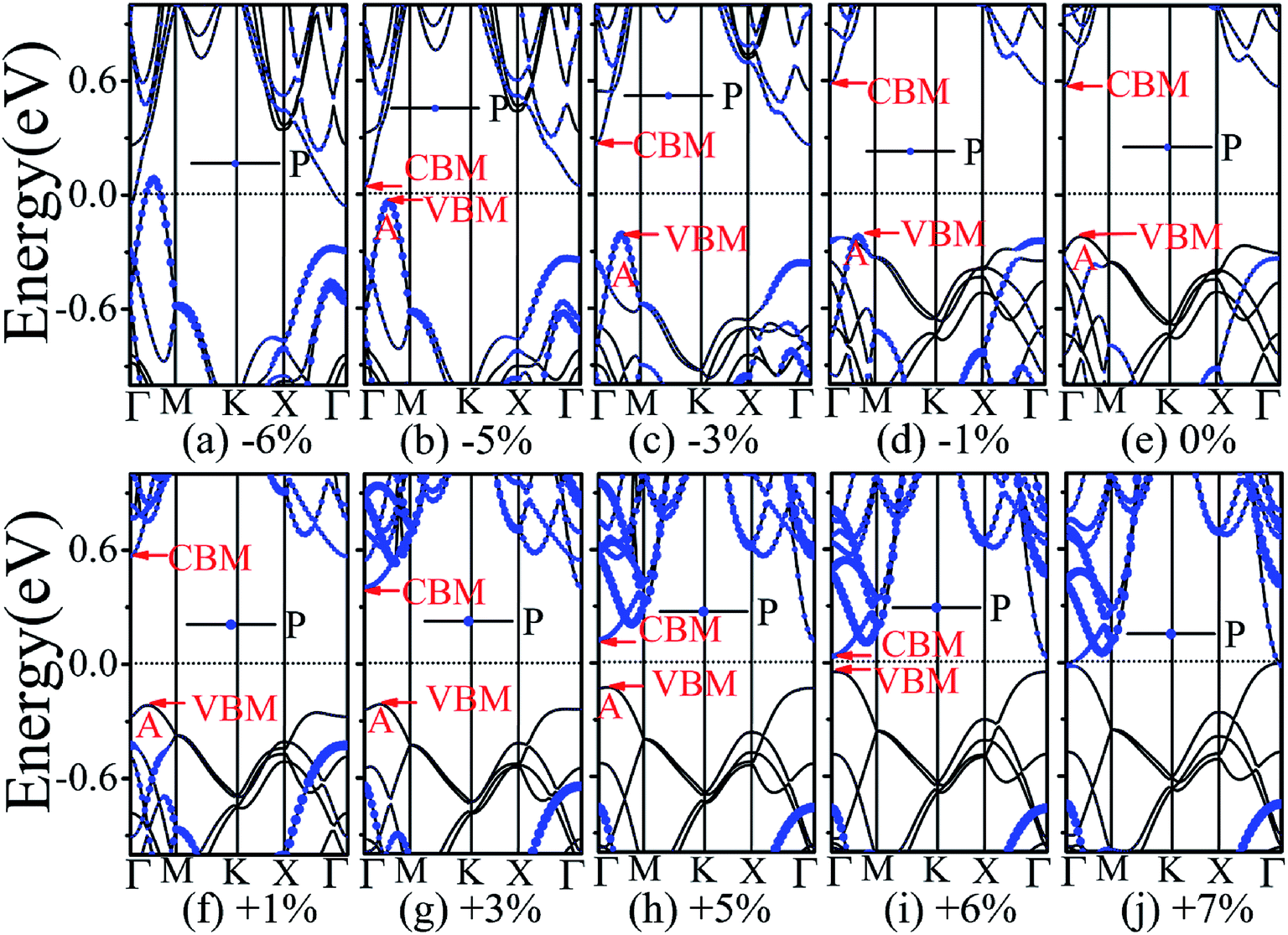 | ||
| Fig. 5 The band structures of the BP/Tl2S with different biaxial uniform strain. | ||
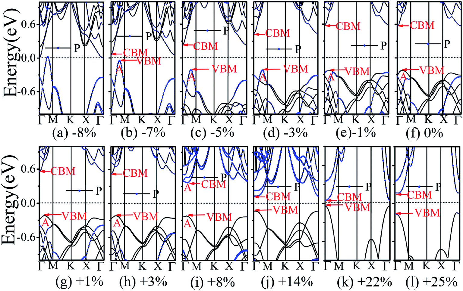 | ||
| Fig. 6 The band structures of the BP/Tl2S with different strain along the x direction strain. | ||
 | ||
| Fig. 7 The band structures of the BP/Tl2S with different strain along the y direction. | ||
In addition, we find an interesting semiconductor–metal and indirect–direct transition of energy gap under suitable strain. In detail, for the strain applied in the biaxial uniform situation in Fig. 5, the VBM moves from A point to Γ point gradually with an increase of tensile strain, while the CBM keeps at Γ point. Hence, the band gap undergoes indirect–direct transition under +6% tensile strain (see Fig. 5(i)). The CBM moves down and goes through the Fermi level at +7% tensile strain (see Fig. 5(j)), resulting the metal character. In the case of stress strain, the gap maintains indirect all through. The indirect band gap converts to zero at −6% stress strain (see Fig. 5(a)), making the BP/Tl2S becoming metal. Interestingly, the CBM is contributed by BP, while the VBM is contributed by Tl2S under tensile strain. Inversely, the CBM is mainly from Tl2S and the VBM is entirely from the BP under the stress strain. Hence, the CBM and VBM of the BP/Tl2S are provided by two different materials in the biaxial uniform situation, which implies a distinct type-II band alignment. For the strain applied in the x direction, the band gap is indirect with the VBM at A point and CBM at Γ point under stress strain of −8% to 0% (see Fig. 6). Once the stress strain exceeds −8%, the band gap changes to zero, inducing that the BP/Tl2S becomes metal. In the case of tensile strain, the band gap is still indirect with the VBM at A point, while the CBM shifted from Γ to A under stress strain above +8%, indicating an indirect-to-direct gap transition at +8% (see Fig. 6(i)). Interestingly, the CBM and VBM simultaneously move in the opposite direction, namely, shift from A point to Γ point little by little in the range of +8% to +14%. Hence, the band gap is direct with the CBM and VBM at Γ point under stress strain above +14%. The band gap downgrades to minimum (0.011 eV) at +22%, then increases rapidly almost tenfold (0.11 eV) at +25% (see Fig. 6(k) and (l)).
Surprisingly, there also exists the band arrangement transition. The BP/Tl2S is still type-I under −1% to +3%, due to both the CBM and VBM of the BP/Tl2S lying in absolutely Tl2S. Furthermore, with further increase of the strain, the BP/Tl2S becomes type-II semiconductor, because the VBM are from the BP, and the CBM comes from Tl2S under the stress strain below −3%, while the source of CBM and VBM appears opposite phenomenon under stress strain above +8%, which can be clearly seen in Fig. 6(i)–(l). For the strain applied in the y direction, with an increase of stress strain, the energy of Γ point is higher than that of A point at −3% (see Fig. 7(e)), indicating an indirect-to-direct gap transition. Then the band gap transitions back to indirect at −6% (see Fig. 7(d)). The band gap becomes zero at −17% (see Fig. 7(a)), and the BP/Tl2S turns into metal. On the side of tensile strain, the VBM is always located at A point, however, the CBM undergoes an interesting transition from Γ to B at +7% (see Fig. 7(j)). Therefore, the band gap remains indirect under tensile strain. It is clear that the BP/Tl2S displays the metallic feature due to the CBM moving down and crossing the Fermi level at +9% (see Fig. 7(l)). What's more, we also find meaningfully the band arrangement transition. For example, both the CBM and VBM of BP/Tl2S are completely localized on Tl2S under −3% to +3% (see Fig. 7(e)–(i)), which emerges a natural type-I band arrangement. Furthermore, with the further increase of strain, the type-I heterostructure transforms to type-II because the VBM and CBM are from the both different material of the BP/Tl2S, which can be carefully confirmed in Fig. 6.
3.2 BP/Tl2S with TM atoms intercalated
From a technical point of view, defects,49,50 adatom adsorption,51–53 and chemical decorations54,55 are all fundamentally and widely employed techniques for tuning the electronic and magnetic properties of 2D materials. Recently, it is reported that intercalating impurity atoms between layers of heterostructures also is an effective strategy to drive magnetism.56 Therefore, we focus on intercalating TMs (3d and 4d) in the BP/Tl2S (TM-BP/Tl2S) to investigate their electronic and magnetic properties. Firstly, we determine the most stable position of the 3d TMs in BP as well as 4d TMs. By comparing adsorption energies of 4d TMs on the three possible adsorption sites (on top of P (T), on top of the hexagonal hollow site (H) and on top of the bridge site of P–P bond (B)), it is found that the H site is the preferable adsorption site with the lowest binding energies (3.47 eV, 5.98 eV, 4.14 eV, 3.15 eV, 4.32 eV, 5.08 eV, 4.95 eV, 3.42 eV, 1.12 eV, 0.13 eV for Y to Cd, respectively). As for 3d TMs, Kulish et al. have performed a systematic study on the binding energy, geometry, and electronic structure of BP with adsorption of 3d TMs.57 The results show that the H site is also energetically favors due to the adsorption energies being the largest for all the TMs.Then, we place the monolayer Tl2S on top of the BP with one TM adsorbed (Fig. 1(e)). In order to search for the favorable intercalating position and optimize the interlayer distance (d) of TM-BP/Tl2S, we employ the following method: we investigate the optimal relative in-plane position by shifting the Tl2S layer at first with a fixed layer distance, at the same time, TM is allowed to move freely between layers, and then we relax and optimize the layer distance with the optimized relative in-plane position. To theoretically estimate the structural stability of the TM-BP/Tl2S systems, the binding energies (EbTM) of TM in TM-BP/Tl2S systems are calculated using the following formula:
| EbTM = E(TM-BP/Tl2S) − E(BP) − E(Tl2S) − E(TM) | (5) |
| EbTM (eV) | Eb (eV) | dTM−Tl (Å) | dTM−P (Å) | d1 (Å) | d2 (Å) | d (Å) | QTM (e) | QP (e) | QTl2S (e) | Egap (eV) | |
|---|---|---|---|---|---|---|---|---|---|---|---|
| Sc | 4.32 | 3.43 | 2.98 | 2.55 | 1.74 | 1.39 | 3.12 | −1.344 | 1.098 | 0.246 | 0(M) |
| Ti | 6.11 | 3.41 | 2.86 | 2.51 | 1.52 | 2.03 | 3.56 | −1.089 | 1.013 | 0.076 | 0(M) |
| V | 4.31 | 2.68 | 2.79 | 2.44 | 1.41 | 1.94 | 3.35 | −0.835 | 0.886 | −0.051 | 0(H) |
| Cr | 2.71 | 1.66 | 2.68 | 2.51 | 1.44 | 2.15 | 3.59 | −0.640 | 0.713 | −0.073 | 0(H) |
| Mn | 3.05 | 1.78 | 2.6 | 2.40 | 1.22 | 2.19 | 3.41 | −0.463 | 0.617 | −0.154 | 0(H) |
| Fe | 4.76 | 2.70 | 2.77 | 2.41 | 1.20 | 2.02 | 3.22 | −0.224 | 0.436 | −0.212 | 0.42(I) |
| Co | 5.42 | 3.56 | 2.55 | 2.15 | 0.85 | 2.40 | 3.25 | 0.010 | 0.246 | −0.256 | 0(M) |
| Ni | 5.49 | 4.09 | 2.55 | 2.38 | 1.18 | 2.30 | 3.47 | −0.014 | 0.248 | −0.234 | 0.67(I) |
| Cu | 3.03 | 2.18 | 2.57 | 2.31 | 1.20 | 2.24 | 3.44 | −0.189 | 0.382 | −0.194 | 0(M) |
| Y | 5.24 | 3.47 | 3.29 | 2.82 | 2.06 | 1.18 | 3.24 | −1.548 | 1.001 | 0.547 | 0(M) |
| Zr | 6.02 | 5.98 | 3.02 | 2.51 | 1.54 | 1.93 | 3.47 | −1.199 | 1.043 | 0.156 | 0(M) |
| Nb | 6.16 | 4.14 | 2.97 | 2.48 | 1.24 | 2.03 | 3.27 | −0.919 | 1.016 | −0.097 | 0(M) |
| Mo | 5.28 | 3.35 | 2.88 | 2.34 | 1.49 | 1.88 | 3.37 | −0.428 | 0.587 | −0.159 | 0.42(I) |
| Tc | 6.27 | 4.32 | 2.79 | 2.27 | 1.47 | 2.08 | 3.55 | −0.093 | 0.330 | −0.237 | 0.13(I) |
| Ru | 6.55 | 5.08 | 2.22 | 3.20 | 1.22 | 2.24 | 3.46 | 0.184 | 0.053 | −0.237 | 0(M) |
| Rh | 6.24 | 4.95 | 3.45 | 2.26 | 1.29 | 2.26 | 3.55 | 0.278 | −0.02 | −0.258 | 0(M) |
| Pd | 4.36 | 3.42 | 3.46 | 2.39 | 1.23 | 2.08 | 3.31 | 0.205 | 0.048 | −0.253 | 0.74(I) |
| Ag | 1.48 | 1.12 | 2.85 | 2.76 | 2.40 | 1.34 | 3.73 | −0.079 | 0.261 | −0.182 | 0(M) |
It is well known that d-shell electrons of TMs are localized and unstable, which may cause rearrangement of substrate electrons when TMs are adsorbed. Therefore, it is necessary to perform the Bader charge analysis58 to determine the transferred charges between the TMs and BP/Tl2S. The results show that intercalating TMs has a very important impact on the charge redistribution of the BP/Tl2S. As for 3d and 4d TMs, there exists the same following phenomenon in the charge transfer: most of the TMs lose electrons, and the lost charges gradually decrease as the atomic number increases. Specifically, the Co of 3d TM and the Ru, Rh, Pd of 4d obtain charges from the BP/Tl2S (see Table 1). Accordingly, the electrons obtained by BP decrease basically as the atomic number increases from Sc to Ni for 3d TMs (from Y to Ru for 4d TMs). On the contrary, the donated charges by Tl2S increase basically as the atomic number decreases from V to Ni for 3d TMs (from Nb to Pd for 4d TMs). In all TM-BP/Tl2S systems, only the BP layer of Rh-BP/Tl2S system donates a few charges to Rh, leading to p-doping effect on the BP. As for Sc-, Ti-, Y- and Zr-BP/Tl2S systems, TMs transfer charges to BP/Tl2S, which leading to n-doping in the BP/Tl2S.
In order to explore the possible application prospects of the various TM-BP/Tl2S systems, it is quite necessary to study the electronic and magnetic properties of the various TM-BP/Tl2S systems. As shown in Table 2, the most TM-BP/Tl2S (Sc-, Co-, Ni-, Cu-, Y-, Zr-, Nb-, Mo-, Ru-, Rh-, Pd-, Ag-) systems have the ground states with non-spin polarization, while the monolayer BP adsorbed by Sc, Co, Y, Nb, Ru are spin polarized, which indicate that the Tl2S has significant influence on the electronic properties of TM-BP. We notice that the TM-BP/Tl2S (Ti-, V-, Cr-, Mn-, Fe-, Tc-) systems are similar to TM-BP (Ti-, V-, Cr-, Mn-, Fe-, Tc-), possess the spin polarized ground states. Nevertheless, compared with the corresponding magnetic moment values of TM-BP (Ti-, V-, Cr-, Mn-, Fe-, Tc-),57 the magnetic moments of the TM-BP/Tl2S (Ti-, V-, Cr-, Mn-, Fe-, Tc-) systems vary from 0.570 μB to 3.406 μB, which are significantly reduced, owing to the interaction between TMs and BP/Tl2S being stronger than the interaction between TMs and BP, which is verified by the binding energies discussed in Table 1. In addition, it can be seen from Table 2 that the total magnetic moments mainly come from TMs. Furthermore, in order to visualize the magnetic moment distribution of the TM-BP/Tl2S (Ti-, V-, Cr-, Mn-, Fe-, Tc-), we display the spin density distributions in Fig. 8. The distinguishing feature of the magnetic moment contribution is that the magnetic moments are mainly localized on the interlayer TMs for the TM-BP/Tl2S (Ti-, V-, Cr-, Mn-, Fe-, Tc-), and a tiny amount of the magnetic moments are induced by the adjacent P and Tl atoms, which is similar to the above results in Table 2. There exists the same phenomenon of magnetic moment distribution in other systems, such as TM-Tl2S systems,26 TM@(graphene/MS2)56 and so on.
| Mtot (μB) | MTM (μB) | MP (μB) | MTl2S (μB) | |
|---|---|---|---|---|
| Sc | 0 | 0 | 0 | 0 |
| Ti | 0.894 | 0.795 | 0.072 | 0.028 |
| V | 0.872 | 0.902 | −0.038 | 0.007 |
| Cr | 3.406 | 3.356 | 0.003 | 0.047 |
| Mn | 2.679 | 2.644 | −0.017 | 0.052 |
| Fe | 1.788 | 1.657 | 0.021 | 0.109 |
| Co, Ni, Cu | 0 | 0 | 0 | 0 |
| Y, Zr, Nb, Mo | 0 | 0 | 0 | 0 |
| Tc | 0.570 | 0.391 | 0.116 | 0.062 |
| Ru, Rh, Pd, Ag | 0 | 0 | 0 | 0 |
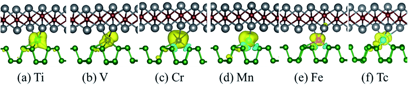 | ||
| Fig. 8 Spin density (up–down) with an isovalue of 0.0025 e Å−3 for six magnetic TM-BP/Tl2S systems: (a) Ti-BP/Tl2S, (b) V-BP/Tl2S, (c) Cr-BP/Tl2S, (d) Mn-BP/Tl2S, (e) Fe-BP/Tl2S, (f) Tc-BP/Tl2S. Yellow and blue indicate the spin up and spin down densities, respectively. | ||
To illustrate the magnetic moment origin of the TM-BP/Tl2S (Ti-, V-, Cr-, Mn-, Fe-, Tc-), we calculate the total density of states (TDOS) and projected density of states (PDOS) of the TMs and its nearest P, Tl and S atoms, as is represented in Fig. 9. It is seen that the TM (Ti, V, Cr, Mn, Fe, Tc) atomic states are dominant near the Fermi level, while few atomic states are from the nearest P, Tl and S atoms, indicating that magnetic moments of these systems (Ti-, V-, Cr-, Mn-, Fe- and Tc-BP/Tl2S) are mainly contributed by the TM d orbital. Moreover, the hybridization between the TM d orbitals and p or s orbitals of the nearest P, Tl atoms occurs in the energy range of −0.9 eV to 0.25 eV, due to energy peaks at the same energy, which results in the splitting of the energy levels near the Fermi level and are responsible for the magnetic moments. Furthermore, the magnetic moments obviously depend on different d orbitals. For Ti-BP/Tl2S system, the Ti-dxy and -dz2 orbitals and the degenerate px, py and pz orbitals of P, px orbitals of Tl hybridize and split at Fermi level, which caused the distinct magnetic moments. For V-, Cr- and Mn-BP/Tl2S systems, they share the similar characteristics that the spin up atomic states have a clear gap while the spin down atomic states occupy the Fermi level, suggesting the half-metallic feature, which agrees with the results of the band structures giving below. However, the magnetic moments are from the different d orbitals, which are dyz, dxy, dz2 of the V atom, dz2, dxz of the Cr atom and dxy, dz2 of Mn atom respectively. For Fe-BP/Tl2S, there exists complicated phenomenon because Fe atom has more than 5 electrons of 3d orbital and some of the nonbonding orbitals are filled. The Fe dyz, dxz orbitals and the degenerate py, pz and s orbitals of P, s orbitals of Tl hybridize and split below Fermi level, while the Fe dx2−y2 orbital and px, s orbitals of P, the degenerate py, px orbitals of Tl hybridize and split above Fermi level. Hence, Fe dyz, dxz and dx2−y2 orbitals mainly contribute to the magnetic moments near the Fermi level. For Tc-BP/Tl2S system, the degenerate dx2−y2, dxz and dyz not only are asymmetrically localized at the Fermi level, but also hybridize with s and p of P and Tl, inducing the magnetic moments. Based on the above analysis of TDOS and PDOS, it is easy to reach the conclusion that the magnetic moments are mainly localized on the TMs, which is agreement with the spin density distribution plotted in Fig. 9.
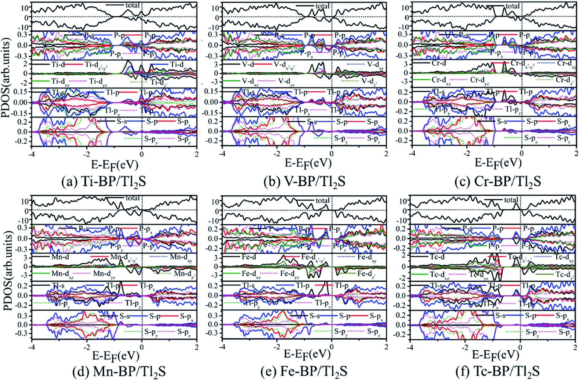 | ||
| Fig. 9 PDOS for six magnetic TM-BP/Tl2S systems: (a) Ti-BP/Tl2S, (b) V-BP/Tl2S, (c) Cr-BP/Tl2S, (d) Mn-BP/Tl2S, (e) Fe-BP/Tl2S, (f) Tc-BP/Tl2S. | ||
Next, we turn to discuss the band structure properties of the various TM-BP/Tl2S systems. We also test the SOC effect on their band structures. Take Ni-BP/Tl2S as an example, the band structures with and without SOC are almost the same (Fig. S3†). So that, the SOC effect is also negligible in TM-BP/Tl2S systems. As mentioned before, the TM-BP/Tl2S (Y-, Zr-, Nb-, Mo-, Ru-, Rh-, Pd-, Ag-, Sc-, Co-, Ni-, Cu-) systems are nonmagnetic since the two spin states match each other (see Fig. 10(a)–(l)). It can be clearly seen from Fig. 10 that the nonmagnetic TM-BP/Tl2S (Y-, Zr-, Nb-, Ru-, Rh-, Ag-, Sc-, Co-, Cu-) systems possess metallic character, because the interaction between TMs and BP/Tl2S make part of energy bands go through the Fermi level. The Ni-, Mo- and Pd-BP/Tl2S systems have no magnetism and still maintain semiconducting features. The indirect band gaps of the Ni-, Mo- and Pd-BP/Tl2S systems are 0.67 eV, 0.43 eV, 0.74 eV, respectively, which are lower than that of the BP/Tl2S. However, the magnetic V-, Cr- and Mn-BP/Tl2S systems have lost their semiconducting nature, and display half-metallic character, because the up and down spin states obviously split and the spin up states maintain semiconducting feature with a narrow band gap, while the spin down states show metallic feature (see Fig. 10(n)–(p)). Moreover, the Tc- and Fe-BP/Tl2S systems show a magnetic semiconducting nature with an indirect band gap (0.13 eV and 0.42 eV), indicating DMS can be obtained by intercalating Tc and Fe in BP/Tl2S, which provide a new route for the potential applications of DMS in spintronic devices.
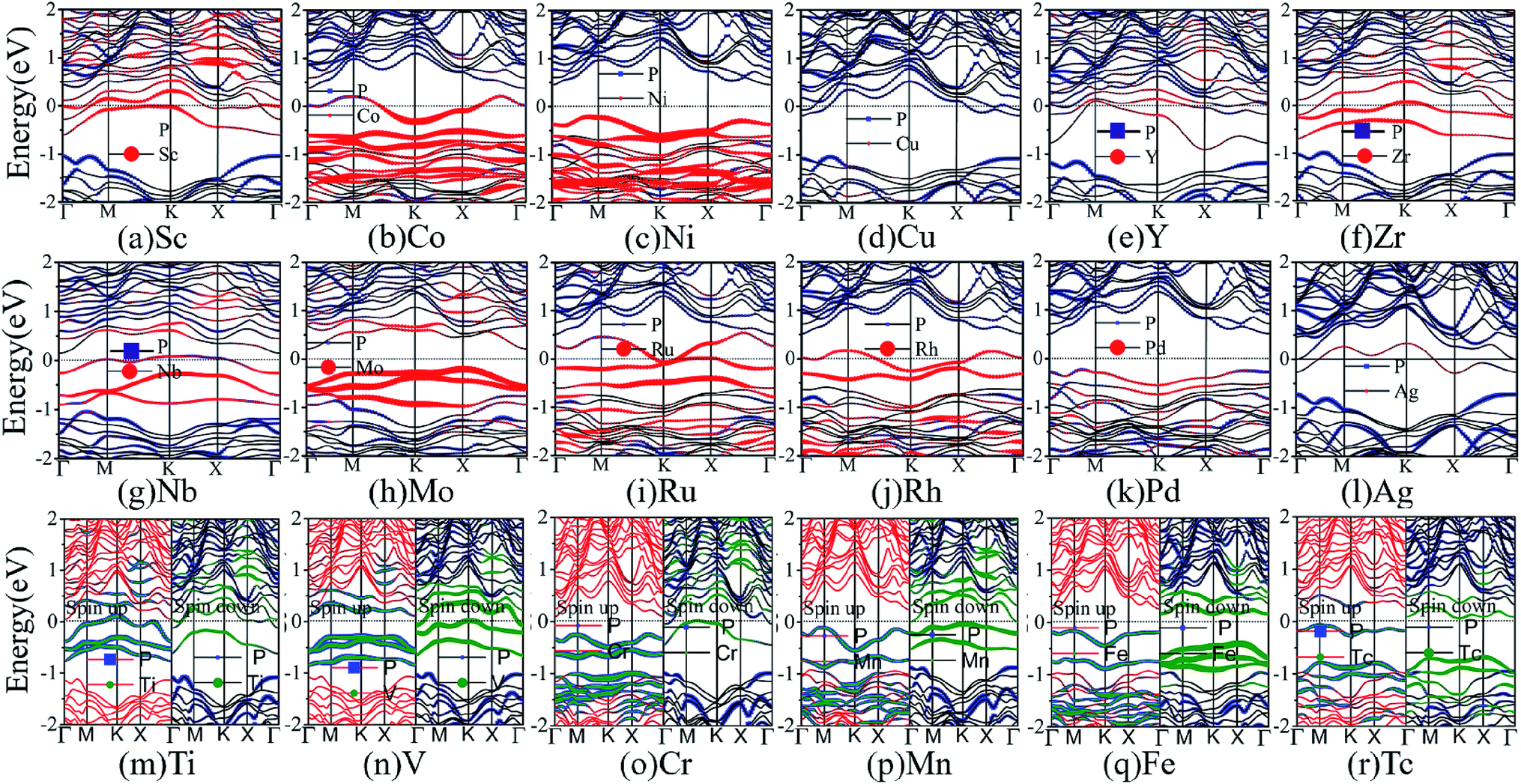 | ||
| Fig. 10 The band structures of the various TM-BP/Tl2S systems: (a) Sc-BP/Tl2S, (b) Co-BP/Tl2S, (c) Ni-BP/Tl2S, (d) Cu-BP/Tl2S, (e) Y-BP/Tl2S, (f) Zr-BP/Tl2S, (g) Nb-BP/Tl2S, (h) Mo-BP/Tl2S, (i) Ru-BP/Tl2S, (j) Rh-BP/Tl2S, (k) Pd-BP/Tl2S, (l) Ag-BP/Tl2S, (m) Ti-BP/Tl2S, (n) V-BP/Tl2S, (o) Cr-BP/Tl2S, (p) Mn-BP/Tl2S, (q) Fe-BP/Tl2S, (r) Tc-BP/Tl2S. | ||
4. Conclusion
In conclusion, we have systematically researched the structural, electronic, and magnetic properties of the BP/Tl2S and the BP/Tl2S with intercalated various TMs by using first-principles calculations. The electronic structure results reveal that the CBM and the VBM of the BP/Tl2S are uniquely dominated by the Tl2S layer of the BP/Tl2S, forming a type-I heterostructure with indirect band gap. Moreover, the band gaps of the BP/Tl2S can be acutely modulated by uniaxial or biaxial uniform strain. The results show that the band gap is more sensitive to biaxial uniform strain than to uniaxial strain. There are the common features that the band gap of the BP/Tl2S experiences an indirect–direct transition regardless of applying uniaxial or biaxial uniform strain. A more interesting thing is that the BP/Tl2S undergoes transitions from type-I to type-II when various strain is applied. Furthermore, in order to enrich and induce the meaningful electronic and magnetic properties of the BP/Tl2S, the BP/Tl2S with intercalated various TMs in the interlayer is studied. Our results show that the electronic and magnetic properties of BP/Tl2S can be widely tuned by TMs intercalated. In all TM-BP/Tl2S systems, there are only six TM-BP/Tl2S (Ti-, V-, Cr-, Mn-, Fe-, Tc-) systems showing robust ferromagnetism. We find the prominent change of the electronic structure induced by TMs intercalated as following: three TM-BP/Tl2S (V-, Cr-, Mn-) systems show a half-metallic nature with 100% spin polarization. The Fe-BP/Tl2S and Tc-BP/Tl2S systems are DMSs. In six TM-BP/Tl2S (Ti-, V-, Cr-, Mn-, Fe-, Tc-) magnetic systems, the Ti-BP/Tl2S system is exception, which shows metallic character. In TM-BP/Tl2S non-magnetic systems, only TM-BP/Tl2S (Mo-, Pd-, Ni-) systems are semiconductors. The other TM-BP/Tl2S systems become metal. The results of the BP/Tl2S and TM-BP/Tl2S systems not only provide experimentally an effective route for designing novel two-dimensional material, but also may present good opportunities for application of the BP/Tl2S and TM-BP/Tl2S in flexible electronics and optoelectronics.Conflicts of interest
There are no conflicts to declare.Acknowledgements
The work was support by the National Natural Science Foundation of China (Grant No. 11404112, U1604131, 61841702), Funding scheme for young teachers in colleges and universities in Henan province (Grant No. 2017GGJS077).References
- J. E. Padilha, A. Fazzio and A. J. R. da Silva, Phys. Rev. Lett., 2015, 114, 066803 CrossRef CAS PubMed.
- N. B. Le, T. D. Huan and L. M. Woods, ACS Appl. Mater. Interfaces, 2016, 8, 6286–6292 CrossRef CAS PubMed.
- W. Yu, Z. Zhu, S. Zhang, X. Cai, X. Wang, C.-Y. Niu and W.-B. Zhang, Appl. Phys. Lett., 2016, 109, 103104 CrossRef.
- L. Huang, Y. Li, Z. Wei and J. Li, Sci. Rep., 2015, 5, 16448 CrossRef CAS PubMed.
- L. Huang, N. Huo, Y. Li, H. Chen, J. Yang, Z. Wei, J. Li and S.-S. Li, J. Phys. Chem. Lett., 2015, 6, 2483–2488 CrossRef CAS PubMed.
- Y. Deng, Z. Luo, N. J. Conrad, H. Liu, Y. Gong, S. Najmaei, P. M. Ajayan, J. Lou, X. Xu and P. D. Ye, ACS Nano, 2014, 8, 8292–8299 CrossRef CAS PubMed.
- G.-H. Lee, Y.-J. Yu, X. Cui, N. Petrone, C.-H. Lee, M. S. Choi, D.-Y. Lee, C. Lee, W. J. Yoo, K. Watanabe, T. Taniguchi, C. Nuckolls, P. Kim and J. Hone, ACS Nano, 2013, 7, 7931–7936 CrossRef CAS PubMed.
- S. Wang, X. Wang and J. H. Warner, ACS Nano, 2015, 9, 5246–5254 CrossRef CAS PubMed.
- R. Gillen, J. Robertson and J. Maultzsch, Phys. Rev. B: Condens. Matter Mater. Phys., 2014, 90, 075437 CrossRef.
- Z. Huang, X. Qi, H. Yang, C. He, X. Wei, X. Peng and J. Zhong, J. Phys. D: Appl. Phys., 2015, 48, 205302 CrossRef.
- Q. Li, L. Xu, K.-W. Luo, L.-L. Wang and X.-F. Li, Mater. Chem. Phys., 2018, 216, 64–71 CrossRef CAS.
- H. V. Phuc, N. N. Hieu, B. D. Hoi and C. V. Nguyen, Phys. Chem. Chem. Phys., 2018, 20, 17899–17908 RSC.
- H. Liu, Z. Huang, G. Wu, Y. Wu, G. Yuan, C. He, X. Qi and J. Zhong, J. Mater. Chem. A, 2018, 6, 17040–17048 RSC.
- L. Li, Y. Yu, G. J. Ye, Q. Ge, X. Ou, H. Wu, D. Feng, X. H. Chen and Y. Zhang, Nat. Nanotechnol., 2014, 9, 372–377 CrossRef CAS PubMed.
- H. Liu, A. T. Neal, Z. Zhu, Z. Luo, X. Xu, D. Tománek and P. D. Ye, ACS Nano, 2014, 8, 4033–4041 CrossRef CAS PubMed.
- S. P. Koenig, R. A. Doganov, H. Schmidt, A. H. Castro Neto and B. Özyilmaz, Appl. Phys. Lett., 2014, 104, 103106 CrossRef.
- S. Das, W. Zhang, M. Demarteau, A. Hoffmann, M. Dubey and A. Roelofs, Nano Lett., 2014, 14, 5733–5739 CrossRef CAS PubMed.
- W. Hu and J. Yang, Comput. Mater. Sci., 2016, 112, 518–526 CrossRef CAS.
- Y. Cai, G. Zhang and Y.-W. Zhang, J. Phys. Chem. C, 2015, 119, 13929–13936 CrossRef CAS.
- N. Gillgren, D. Wickramaratne, Y. Shi, T. Espiritu, J. Yang, J. Hu, J. Wei, X. Liu, Z. Mao, K. Watanabe, T. Taniguchi, M. Bockrath, Y. Barlas, R. K. Lake and C. Ning Lau, 2D Mater., 2014, 2, 011001 CrossRef.
- L. Huang and J. Li, Appl. Phys. Lett., 2016, 108, 083101 CrossRef.
- K. Lee, S. W. Kim, Y. Toda, S. Matsuishi and H. Hosono, Nature, 2013, 494, 336 CrossRef CAS PubMed.
- A. Walsh and D. O. Scanlon, J. Mater. Chem. C, 2013, 1, 3525–3528 RSC.
- T. Inoshita, S. Jeong, N. Hamada and H. Hosono, Phys. Rev. X, 2014, 4, 031023 Search PubMed.
- Q. Wu, J.-J. Zhang, P. Hao, Z. Ji, S. Dong, C. Ling, Q. Chen and J. Wang, J. Phys. Chem. Lett., 2016, 7, 3723–3729 CrossRef CAS PubMed.
- N. Song, Y. Wang, W. Yu, L. Zhang, Y. Yang and Y. Jia, Appl. Surf. Sci., 2017, 425, 393–399 CrossRef CAS.
- S. Shen, Y. Liang, Y. Ma, B. Huang, W. Wei and Y. Dai, Phys. Chem. Chem. Phys., 2018, 20, 14778–14784 RSC.
- A. Andersen, S. M. Kathmann, M. A. Lilga, K. O. Albrecht, R. T. Hallen and D. Mei, J. Phys. Chem. C, 2012, 116, 1826–1832 CrossRef CAS.
- S. Sattar, N. Singh and U. Schwingenschlögl, ACS Appl. Mater. Interfaces, 2018, 10, 4266–4270 CrossRef CAS PubMed.
- Y. Gong, H. Yuan, C.-L. Wu, P. Tang, S.-Z. Yang, A. Yang, G. Li, B. Liu, J. van de Groep, M. L. Brongersma, M. F. Chisholm, S.-C. Zhang, W. Zhou and Y. Cui, Nat. Nanotechnol., 2018, 13, 294–299 CrossRef CAS PubMed.
- Y. Guang, Y. Yanmin, M. Hongran, M. Xiujuan, L. Congcong, L. Jie, Z. Qiang, Z. Zhidong, Y. Fuxing and L. Jia, Nanotechnology, 2018, 29, 115201 CrossRef PubMed.
- G. Kresse and J. Hafner, Phys. Rev. B: Condens. Matter Mater. Phys., 1993, 47, 558–561 CrossRef CAS PubMed.
- G. Kresse and J. Hafner, Phys. Rev. B: Condens. Matter Mater. Phys., 1994, 49, 14251–14269 CrossRef CAS PubMed.
- G. Kresse and J. Furthmüller, Phys. Rev. B: Condens. Matter Mater. Phys., 1996, 54, 11169 CrossRef CAS PubMed.
- J. Klimeš, D. R. Bowler and A. Michaelides, J. Phys.: Condens. Matter, 2009, 22, 022201 CrossRef PubMed.
- J. Klimeš, D. R. Bowler and A. Michaelides, Phys. Rev. B: Condens. Matter Mater. Phys., 2011, 83, 195131 CrossRef.
- N. Song, H. Ling, Y. Wang, L. Zhang, Y. Yang and Y. Jia, J. Solid State Chem., 2019, 269, 513–520 CrossRef CAS.
- W.-B. Zhang, Q. Qu, P. Zhu and C.-H. Lam, J. Mater. Chem. C, 2015, 3, 12457–12468 RSC.
- J. P. Perdew, K. Burke and M. Ernzerhof, Phys. Rev. Lett., 1996, 77, 3865–3868 CrossRef CAS PubMed.
- Y. Li, S. Yang and J. Li, J. Phys. Chem. C, 2014, 118, 23970–23976 CrossRef CAS.
- X. Han, H. Morgan Stewart, S. A. Shevlin, C. R. A. Catlow and Z. X. Guo, Nano Lett., 2014, 14, 4607–4614 CrossRef CAS PubMed.
- G. Giester, C. L. Lengauer, E. Tillmanns and J. Zemann, J. Solid State Chem., 2002, 168, 322–330 CrossRef CAS.
- M. Sun, J.-P. Chou, J. Yu and W. Tang, Phys. Chem. Chem. Phys., 2017, 19, 17324–17330 RSC.
- C. He, M. Cheng and W. Zhang, Mater. Res. Express, 2018, 5, 065059 CrossRef.
- M. M. Dong, C. He and W. X. Zhang, J. Mater. Chem. C, 2017, 5, 3830–3837 RSC.
- J. Qiao, X. Kong, Z.-X. Hu, F. Yang and W. Ji, Nat. Commun., 2014, 5, 4475 CrossRef CAS PubMed.
- M.-Q. Long, L. Tang, D. Wang, L. Wang and Z. Shuai, J. Am. Chem. Soc., 2009, 131, 17728–17729 CrossRef CAS PubMed.
- X. Peng, Q. Wei and A. Copple, Phys. Rev. B: Condens. Matter Mater. Phys., 2014, 90, 085402 CrossRef.
- Z. Zhang, X. Zou, V. H. Crespi and B. I. Yakobson, ACS Nano, 2013, 7, 10475–10481 CrossRef CAS PubMed.
- D. W. Boukhvalov and M. I. Katsnelson, Nano Lett., 2008, 8, 4373–4379 CrossRef CAS.
- E. Kan, H. Xiang, F. Wu, C. Lee, J. Yang and M.-H. Whangbo, Appl. Phys. Lett., 2010, 96, 102503 CrossRef.
- L. Ming-Yang, C. Qing-Yuan, H. Yang, L. Ze-Yu, C. Chao and H. Yao, Nanotechnology, 2018, 29, 095203 CrossRef PubMed.
- V. O. Özçelik, D. Kecik, E. Durgun and S. Ciraci, J. Phys. Chem. C, 2015, 119, 845–853 CrossRef.
- E.-j. Kan, Z. Li, J. Yang and J. G. Hou, J. Am. Chem. Soc., 2008, 130, 4224–4225 CrossRef CAS PubMed.
- Y. Wang and H.-P. Cheng, Phys. Rev. B: Condens. Matter Mater. Phys., 2011, 83, 113402 CrossRef.
- X. Zhang, Z. Bao, X. Ye, W. Xu, Q. Wang and Y. Liu, Nanoscale, 2017, 9, 11231–11238 RSC.
- V. V. Kulish, O. I. Malyi, C. Persson and P. Wu, Phys. Chem. Chem. Phys., 2015, 17, 992–1000 RSC.
- G. Henkelman, A. Arnaldsson and H. Jonsson, Comput. Mater. Sci., 2006, 36, 354–360 CrossRef.
Footnote |
| † Electronic supplementary information (ESI) available. See DOI: 10.1039/c9ra03547h |
| This journal is © The Royal Society of Chemistry 2019 |