
 Open Access Article
 This Open Access Article is licensed under a Creative Commons Attribution-Non Commercial 3.0 Unported Licence
Magnetoelectric coupling tailored by the orientation of the nanocrystals in only one component in percolative multiferroic composites†
Yu Tang ac,
Ruixin Wanga,
Yi Zhang*b,
Bin Xiaod,
Shun Lia and
Piyi Du*c
ac,
Ruixin Wanga,
Yi Zhang*b,
Bin Xiaod,
Shun Lia and
Piyi Du*c
aDepartment of Materials Science and Engineering, College of Aerospace Science and Engineering, National University of Defense Technology, Changsha 410073, China
bDepartment of Physics, College of Liberal Arts and Sciences, National University of Defense Technology, Changsha 410073, China. E-mail: zhangyi1983@zju.edu.cn
cState Key Laboratory of Silicon Materials, School of Materials Science and Engineering, Zhejiang University, Hangzhou 310027, China. E-mail: dupy@zju.edu.cn
dDepartment of Materials Science and Engineering, Shenzhen Engineering Research Center for Novel Electronic Information Materials and Devices, Southern University of Science and Technology, Shenzhen 518055, China
First published on 1st July 2019
Abstract
Novel 1–3 type multiferroic composite thin films were prepared via a simple 0–3 composite fabrication process. The orientation of the Ni0.5Zn0.5Fe2O4 (NZFO) nanocrystals in the BaTiO3–Ni0.5Zn0.5Fe2O4 (BTO–NZFO) composite thin films was controlled by magnetron sputtering, and the controlling effect of such orientation on magnetoelectric coupling was investigated in detail. The NZFO lattice in the BTO–NZFO composite thin films grew with (100) orientation under the induction of the (111) plane of Si. The transfer of substrate stress between the closely contacted grains also contributes to the orientation of the NZFO nanocrystals. The 0.6BTO–0.4(100)NZFO multiferroic composite thin film exhibited a magnetization strength of 9.2% at the Curie point of the BTO phase, showing extremely strong magnetoelectric coupling characteristics. This work provides an effective strategy for the development of high-performance multiferroic composites, and brings about new conception of realizing strong magnetoelectric coupling effect from the perspective of physical chemistry.
Introduction
Multiferroics are one of the most promising candidates for next-generation electronic devices, characterized by the coexistence of multiple ferroicity such as ferroelectricity and ferromagnetism as well as the magnetoelectric coupling effect between them. These intriguing properties enable multiferroic composites to be potentially applied in the fields where high-density signal storage and multi-state responses are required.1–4 Compared with single-phased multiferroics, which is rare in nature and difficult to achieve the coexistence of ferroelectricity and ferromagnetism theoretically,5 multi-phased multiferroics, especially multiferroic composite thin films, are becoming the research hotspot in the family of functional materials during the past decades.6–9According to strain coupling mechanism, a strong magnetoelectric coupling in a multiferroic composite is resulted from the anisotropic strain transmitted between the two constituent phases,10 usually requiring an anisotropy contact between them. It suggests that there is a normal interface between the two phases without a radial interface. Therefore, among the three common composite structures of multi-phased multiferroics, i.e. particulate composite (0–3 type), layered composite (2–2 type), and columnar composite (1–3 type),10 1–3 type composites with a larger anisotropic interface should theoretically exhibit a stronger magnetoelectric coupling effect, which has been confirmed by Zheng et al.11,12
However, compared with the 1–3 structure that is generally formed by 1D ferromagnetic/ferroelectric nanowires embedded in a 3D ferroelectric/ferromagnetic matrix, the 0–3 structure composed of 0D ferromagnetic/ferroelectric particles dispersed in a 3D ferroelectric/ferromagnetic matrix possesses obvious advantages of easy control and repeatable fabrication.13,14 According to percolation theory and the calculation results from random occupancy model, the percolation thresholds for two-dimensional (2D) and three-dimensional (3D) materials are 0.45 and 0.16, respectively.15,16 It means that a percolation channel constructed by the interconnecting crystals will form in the composite thin films whose radial and normal directions exhibit two-dimensional and three-dimensional characteristics, respectively, as long as the content of the ferromagnetic or electrical phase is controlled between the percolation thresholds of the 2D and 3D systems. In light of this, a structure similar to 1–3 composite structure could probably be achieved via 0–3 process.
After the idea that 1–3 composite structure can be realized in percolative nanocomposites through 0–3 process was demonstrated and validated by their magnetic and electric performances,17 how to further improve the magnetoelectric coupling of the composites becomes the next question. As is known, for 1–3 multiferroic composites, the ferromagnetic lattices may subject to anisotropic stress, even the neighboring ferroelectric lattices are disordered as long as they can shrink or expand under changing external field. This effect will lead to an anisotropic deformation of the ordered ferromagnetic lattices and the rotation of the magnetic dipoles, and thus a change in macroscopic magnetization strength. Therefore, the oriented growth of all components is not necessary for the occurrence of magnetoelectric coupling effect, although the components in previously reported 1–3 multiferroic composites were all oriented. By tailoring the anisotropy of the lattice strain in 1–3 composites, magnetoelectric coupling can be possibly achieved in multiferroic composites with oriented ferromagnetic phase and random ferroelectric phase. Furthermore, the ferroelectricity and ferromagnetism of the multiferroic composites can also get improved by controlling the orientation of the component phase. In this context, the realization of the ordered growth of the ferromagnetic phase by traditional 0–3 process is the key to obtain multiferroic composites with the high magnetoelectric coupling performance via a simple fabrication process, which is definitely favorable of large-scale industrial applications.
Herein, a typical multiferroic composite material, BaTiO3(BTO)–Ni0.5Zn0.5Fe2O4(NZFO) thin films, were prepared by magnetron sputtering, which has been widely used in industrial deposition process and is favorable of large-scale industrial production. It should be noted that the BTO–NZFO nanocomposite is a well-known composite system, on which plenty of studies has been carried out involving their preparation, structure and properties, but there is no research on the orientation of only one constituent phase and its effect on magnetoelectric coupling to the best of our knowledge.18–21 The effects of sputtering power and sputtering atmosphere on the growth of the NZFO phase in the films were investigated systematically. In light of the experimental results, the underlying physical and chemical mechanisms were revealed. In the meantime, an effective strategy to prepare high-performance BTO–(100)NZFO composite thin films by magnetron sputtering was provided. More importantly, it demonstrated that the magnetoelectric coupling can be tailored by the orientation of the nanocrystals of only one component in percolative multiferroic composites.
Experimental section
The BTO–NZFO composite thin films were prepared by a magnetron sputtering system (JGP-560, Sky Technology Development) using a BTO–NZFO composite-ceramic target. The sputtering targets with different molar ratios of BTO to NZFO were solid-phase sintered at 1200 °C for 2 h in powder state, which were prepared by in situ sol–gel process and citric acid combustion method. The sputtering atmosphere was set as the mixture of 0.4O2 and 0.6Ar2 with a total pressure of 0.6 × 10⁻³ mbar, and the sputtering power was controlled in the region between 80 W and 250 W. The sputtering time was chosen as 2–6 h in order to keep the films to possess an approximately identical thickness value of ∼100 nm. The sputtering substrate included the (100) and (111) oriented single-crystal silicon treated by two different cleaning methods. In the first cleaning method (Process 1), the cut single-crystal silicon substrate with a size of 25 mm × 45 mm × 1 mm was preliminarily cleaned with deionized water, immersed in a washing solution of hydrofluoric acid with a concentration of 10% for 10 min, cleaned with deionized water again for three times, and then placed in acetone and anhydrous ethanol under ultrasonically cleaning for 0.5 h. In the second method (Process 2), the single-crystal silicon was only ultrasonically cleaned with ethanol and deionized water.To investigate the influence of different steps in the process, the samples were not heated in situ during the above-mentioned sputtering process and the sputtering chamber is cooled by circulating cooling water. After the deposition step was finished, the deposited films were annealed in a muffle furnace (L5/11/P330, Nabertherm) at a temperature of 600–820 °C.
The thickness of the films were measured by the thin-film analyzer (F20, Filmetrics). The lattice information of the xBTO–(1−x)NZFO composite thin films were analyzed by X-ray diffraction (XRD, D8 ADVANCE DA VINCI, Bruker) with Grazing Incidence Diffraction (GID) technology. The step size and scanning rate of XRD were 0.01° and 2° min−1, respectively. The microstructure of the films were characterized by scanning electron microscopy (SEM, FESEM-SIRION-100, FEI) and transmission electron microscopy (TEM, Tecnai G2 F20, FEI). The samples for SEM observation were slices containing films and substrate with a superficial area of 2 mm × 2 mm, yet those for TEM observation were the films scraped by edge from substrate. The LakeShore 7407 vibrating sample magnetometer (VSM, Lakeshore) with a resolution of 10−7 emu was used to test the magnetic strength of the composite films in the temperature range of 300–1273 K. All the samples were ultrasonically cleaned in ethyl alcohol for 0.5 h before measurement.
Results and discussion
The XRD patterns of the xBTO–(1−x)NZFO (x = 0.2–1.0) composite thin films deposited on (100)- and (111)-oriented silicon substrates and sintered at 800 °C are shown in Fig. 1(a) and (b). As can be seen, besides the diffraction peaks of the silicon substrate, the diffraction peaks of perovskite BTO and spinel NZFO were also observed without any impurity phase. The NZFO nanocrystals in all composite thin films deposited on (111)-oriented Si substrate exhibited a distinct (100) orientation; on the contrary, there is no specific orientation for the NZFO nanocrystals in the composites deposited on (100)-oriented Si substrate. Comparatively, the BTO phase in the composites exhibited a completely random orientation on both substrates, i.e. regardless of the orientation of the Si substrate. In addition, compared with the XRD pattern of the sputtering target, the peaks corresponding to the BTO phase on the (100)-oriented Si substrate shift to lower angle but those on the (111)-oriented Si substrate remained unchanged,22 which is in obvious contrast to the phenomenon that the peaks of the NZFO phase on both substrates all shift to higher angles.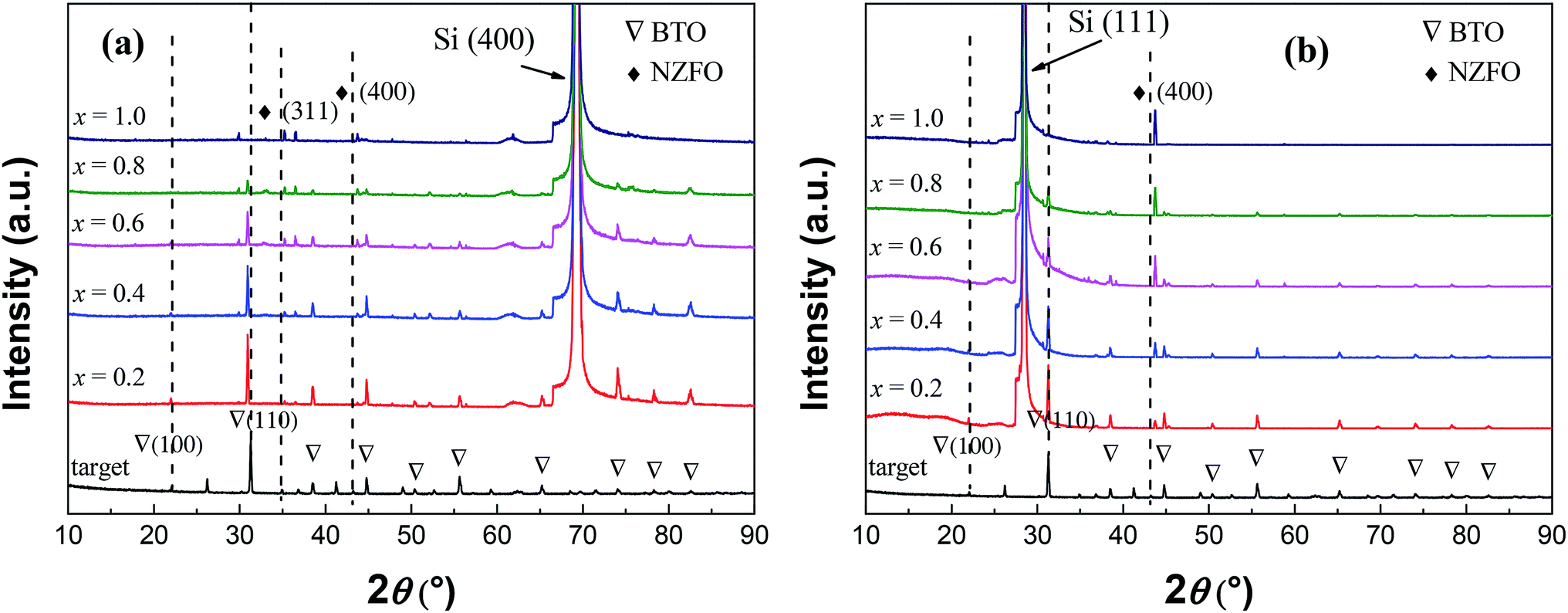 | ||
| Fig. 1 XRD patterns of the (1−x)BTO–xNZFO composite thin films deposited on (a) (100)- and (b) (111)-oriented Si substrates,22 and the sputtering target. | ||
Fig. 2 shows the SEM and TEM images of the surface of 0.6BTO–0.4NZFO composite thin films on (100) and (111)-oriented Si substrates.22 The fine crystalline grain with a size of ∼20 nm can be distinguished in both films with a thickness of ∼100 nm. While the surface morphologies of the composite films deposited on different substrates are similar, the orientation of the constituent grains, i.e. the NZFO grains, is different. Unlike the randomly-oriented NZFO on the (100)-oriented Si substrate (Fig. 2(c)), the NZFO on the (111)-oriented Si substrate exhibited a clear (100) orientation (Fig. 2(d)).
 | ||
| Fig. 2 (a and b) SEM and (c and d) TEM images of the surface of 0.6BTO–0.4NZFO composite thin films on (100) and (111)-oriented Si substrates. | ||
According to the Bragg equation, the shift of the diffraction peaks in the XRD pattern indicates a change in the interplanar spacing in the vertical direction. The shift to lower and higher angle means an increase and decrease in the interplanar spacing, respectively. Hence, the shift of the diffraction peaks of the BTO phase on the (100)-oriented Si substrate to lower angle indicates that the interplanar spacing increases in the normal direction. The shift of the peaks of the NZFO phase on the (111)-oriented Si substrate to higher angle indicates that the interplanar spacing decreases. It suggests that there are interactions between the substrate and the crystalline phases of the thin films, which caused the lattice of BTO and NZFO in the composite to change. Obviously, this interaction is related to the structures of the substrate and the constituent phases.
As is already known, Si has a cubic diamond structure belonging to the Fd![[3 with combining macron]](https://www.rsc.org/images/entities/char_0033_0304.gif) m space group. In this scenario, the Si atom occupies the 8a (0, 0, 0) position as shown in Fig. 3(a).23 In perovskite BTO structure, which belongs to the Pmm (No. 221) space group, the atomic positions of Ti and Ba are 1a (0, 0, 0) and 1b (1/2, 1/2, 1/2), respectively, while the O ion occupies the 3c (1/2, 1/2, 0) position as shown in Fig. 3(d).23 In spinel ferrite whose space group is Fdm (No. 227), the oxygen atom occupies each lattice point of the eight small cubes constituting the unit cell, i.e., the Wyckoff position of 32e (3/8, 3/8, 3/8). There are two types of positions for transition metal ions: the oxygen tetrahedral (A-site) and octahedral (B-site) interstices. The Wyckoff positions of A and B are Td (0, 0, 0) and Oh (5/8, 5/8, 5/8) as shown in Fig. 3(g).23 Therefore, the chemical formula of the ferrite with spinel structure is commonly written as AB2O4. The atomic occupancy on the (800) and (311) planes of the spinel ferrite, the (110) plane of the perovskite ferroelectrics, and the (100) and (111) planes of Si are displayed in Fig. 3(b)–(f). The spacing of the two atoms perpendicular to each other on these crystallographic planes are summarized in Table 1.23
m space group. In this scenario, the Si atom occupies the 8a (0, 0, 0) position as shown in Fig. 3(a).23 In perovskite BTO structure, which belongs to the Pmm (No. 221) space group, the atomic positions of Ti and Ba are 1a (0, 0, 0) and 1b (1/2, 1/2, 1/2), respectively, while the O ion occupies the 3c (1/2, 1/2, 0) position as shown in Fig. 3(d).23 In spinel ferrite whose space group is Fdm (No. 227), the oxygen atom occupies each lattice point of the eight small cubes constituting the unit cell, i.e., the Wyckoff position of 32e (3/8, 3/8, 3/8). There are two types of positions for transition metal ions: the oxygen tetrahedral (A-site) and octahedral (B-site) interstices. The Wyckoff positions of A and B are Td (0, 0, 0) and Oh (5/8, 5/8, 5/8) as shown in Fig. 3(g).23 Therefore, the chemical formula of the ferrite with spinel structure is commonly written as AB2O4. The atomic occupancy on the (800) and (311) planes of the spinel ferrite, the (110) plane of the perovskite ferroelectrics, and the (100) and (111) planes of Si are displayed in Fig. 3(b)–(f). The spacing of the two atoms perpendicular to each other on these crystallographic planes are summarized in Table 1.23
 | ||
| Fig. 3 Lattice structure of (a) diamond silicon, (b) (100), and (c) (110) planes of silicon; (d) perovskite BTO, (e) (100), and (f) (110) planes of BTO; (g) spinel NZFO, (h) (311), and (i) (800) planes of NZFO. | ||
| a1 (Å) | a2 (Å) | |
|---|---|---|
| Si(100) | 3.84 | 3.84 |
| Si(111) | 3.84 | 6.651 |
| BTO(100) | 4.017 | 4.017 |
| BTO(110) | 4.017 | 5.685 |
| NZFO(311) | 3.637 | 5.94 |
| NZFO(800) | 3.626 | 6.641 |
In general, the growth of the thin films will be affected by the stress arising from the substrate that has a different lattice structure.24 When the atomic spacing of the substrate crystals is smaller than that of the thin films, the substrate will exert compressive stress along the surfaces of the thin films to reduce atomic spacing. On the contrary, the surfaces of the thin films will be imposed to a tensile stress if the substrate crystals are larger. As a consequence, the stress caused by the lattice mismatch between the substrate and the thin films will give rise to a radial shrinkage or expansion of the lattice of the thin films towards the substrate lattice.
Generally speaking, if the stress causes the lattice to shrink in one direction, it will also cause the lattice to expand in the other direction25 (Fig. 4). Compared with the atomic spacing of Si on the (100) plane, those of the BTO lattice on some main planes including (100) and (110) are larger, and those of the NZFO lattice on the (311) and (800) planes are smaller, as shown in Table 1. Therefore, the stress from the (100)-oriented Si substrate causes the BTO lattice in the composite thin films to shrink radially and expand in the normal direction, and the NZFO lattice to expand in the radial direction and shrink in the normal direction as shown in Fig. 1(a). Moreover, as shown in Table 1, unlike the a1 and a2 of the BTO lattice, whose values on different planes are obviously larger and smaller than those of the (111) plane of Si, respectively, both a1 and a2 of the NZFO lattice on the (800) plane are just slightly smaller. It is speculated that the stress on the BTO lattice on the (111)-Si contains both tensile and compressive stress, thus causing the BTO lattice to remain relatively unchanged overall owing to the counteracting of the two stresses. Nevertheless, a radial tensile stress from (111)-Si is applied on the (800) plane of the NZFO lattice, causing it to expand radially and contract in the normal direction as shown in Fig. 1(b).
 | ||
| Fig. 4 Schematic diagram illustrating the deformation of the thin film lattice caused by the mismatch between the thin film and the substrate. | ||
It has been revealed in previous researches that the strain energy caused by lattice deformation will increase the crystallization activation energy and then restricts the crystallization of the thin films.24 Therefore, the crystallization activation energy of the phase that has a large difference in the structure from that of the substrate lattice is large, and the crystallization's possibility is small under the same preparation conditions. Moreover, the similarity between the lattices of the thin films and the substrate will result in the order growth of the lattice of the thin films toward the lattice plane of the substrate, especially in the bottom region. As shown in Table 1, except that the difference in the average atomic spacing of the (111) plane of Si and the (800) plane of NZFO is only 2.86%, the difference is larger than 4.5% for most of the planes of Si, BTO and NZFO lattices. It is responsible for the growth of the NZFO nanocrystals in the composite thin films on the (111)-Si substrate with (800), i.e. (100) orientation, and the random growth of the BTO crystals on the (111)-Si, as well as the BTO and NZFO nanocrystals on the (100)-Si, as shown in Fig. 1(a) and (b), which is in accordance with previous researches.22,26
It should be noted that different cleaning processes will probably result in different conditions of the film substrates. For example, hydrofluoric acid can effectively remove the oxides on the surface of single-crystal silicon.27,28 Fig. 5 presents the XRD patterns of 0.2BTO–0.8NZFO composite thin films on the (111)-Si substrate cleaned by Process 1 and Process 2, which are denoted as S1 and S2, respectively. All the diffraction peaks of S1 can be assigned to BTO, NZFO and Si. Particularly, the NZFO phase exhibited a distinct (100) orientation. By contrast, the diffraction peaks corresponding to SiO2 and other crystal planes of NZFO can also be observed in the XRD pattern of S2.
 | ||
| Fig. 5 XRD patterns of 0.2BTO–0.8NZFO composite thin film deposited on the (111) silicon substrate cleaned via Process 1 and 2. | ||
The cross-sectional SEM images of S1 and S2 are displayed in Fig. 6(a) and (b), respectively. Obviously, the substrate cleaned via Process 1 contacts closely with the deposited thin films, while there is a SiO2 layer with ∼100 nm in thickness between the Si substrate and the thin film via Process 2.
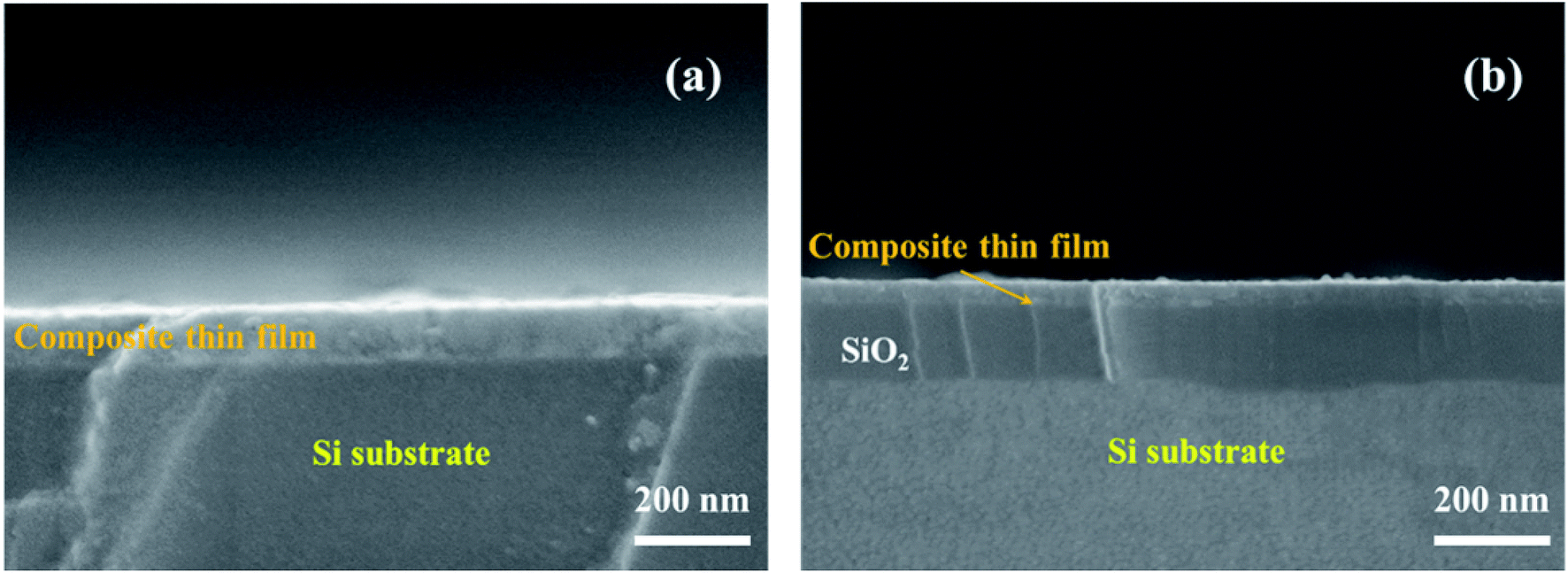 | ||
| Fig. 6 SEM images of the cross-section of 0.2BTO–0.8NZFO composite thin film deposited on the (111) Si substrate cleaned via methods 1 and 2. | ||
As discussed above, the close contact between the lattices of the substrate and the thin film would generate an interaction between them. Hence, this interaction will disappear when the two lattices could not contact each other. It is reasonable to believe that the presence and absence of the SiO2 layer between the composite thin film and the substrate directly depends on the orientation of NZFO, as shown in Fig. 5 and 6. In other words, the existence of SiO2 layer further proves that the formation of the (100)-NZFO is closely related to the induction from (111)-Si substrate.
Fig. 7 shows the XRD patterns of (1−x)BTO–xNZFO composite thin films on the (111)-Si cleaned via Process 1 at different sputtering powers of 80 W, 120 W, 140 W, 160 W, 200 W, and 250 W, respectively. All of the samples were sintered at 800 °C. When the sputtering power is less than 100 W, the diffraction peaks of NZFO can be assigned to many different planes including (220), (311), (222), and (400). As the sputtering power increases from 100 W to 200 W, the peak intensity of the (400) plane becomes stronger, while that of other peaks gradually weaken down. When the sputtering power reaches 200 W, only the peaks of the (400) plane can be observed for NZFO. However, when the sputtering power increases to 250 W, the peaks corresponding to other planes such as (311) appears again. In contrast, the change in sputtering power does not have a significant effect on the growth of the BTO phase in the composite.
 | ||
| Fig. 7 XRD patterns of the (1−x)BTO–xNZFO composite thin films deposited on (111) Si substrate prepared by RF magnetron sputtering with a sputtering power of (a) 80 W, (b) 100 W, (c) 120 W, (d) 160 W, (e) 200 W, and (f) 250 W. | ||
Fig. 8(a) shows the XRD patterns of S1 at a sputtering power of 200 W and a sintering temperature range of 720–840 °C. As the sintering temperature T increases in the range of 720–800 °C, there is no significant change in the peak intensity of BTO but those of NZFO become much stronger. Meanwhile, the ratio of the peak intensity of each plane in the ferrite also changes with sintering temperature. Fig. 8(b) shows the intensity ratio of the (400) peak to all peaks of NZFO in the composite thin films (denoted as INZFO(400)/INZFO) as a function of sintering temperature. As can be seen, the value of INZFO(400)/INZFO increases first and then decreases afterwards when T increases from 720 °C to 840 °C exhibiting a maximum value of ∼100% at T = 800 °C.
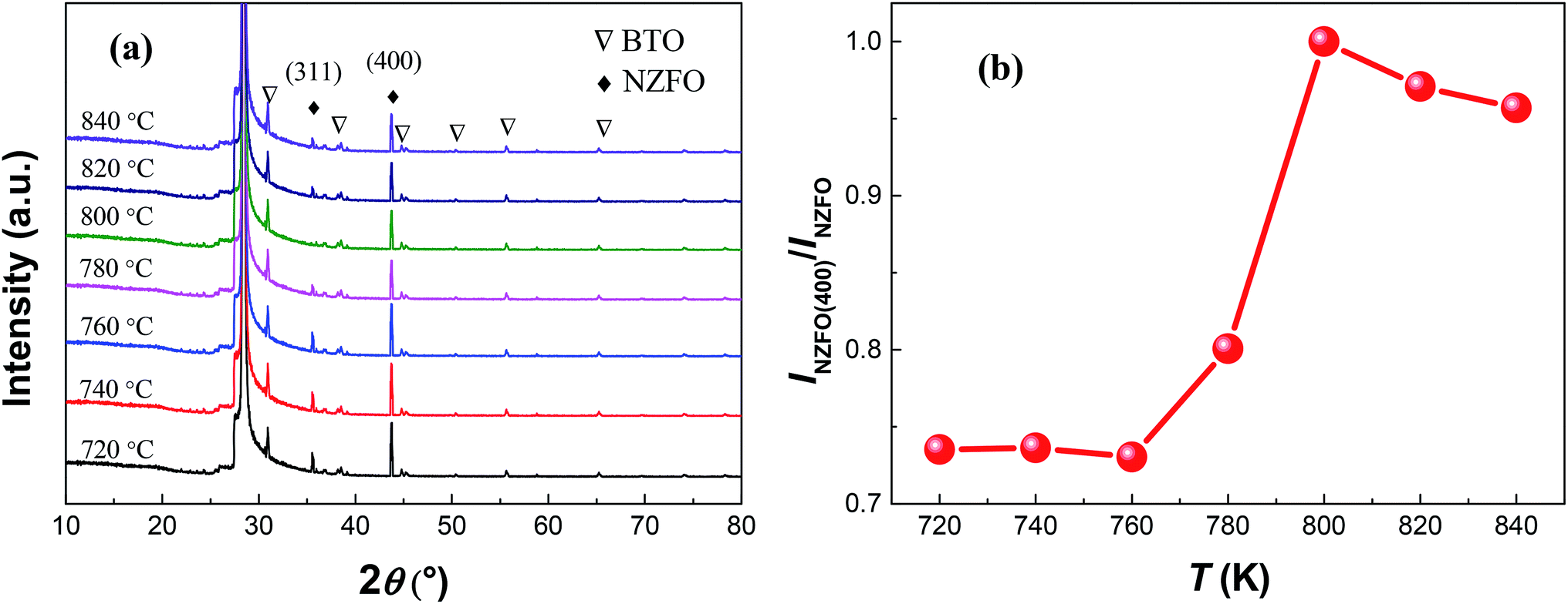 | ||
| Fig. 8 (a) XRD patterns of the 0.2BTO–0.8NZFO composite thin films on (111) Si substrate prepared by magnetron sputtering with a sputtering power of 200 W and various sintering temperatures. (b) The intensity ratio of the (400) peak to all diffraction peaks of the NZFO phase as a function of sintering temperature. | ||
Referring to previous analysis, it can be interpreted that when the sputtering power is small than 200 W, the atomic spacing of the deposited atoms on the substrate decreases as the sputtering power increases, and the density of the BTO–NZFO composite thin films increases as well.25 When the sputtering power reaches 200 W, the minimum potential for the atomic spacing and the maximum density of the thin films can be obtained, which remain unchanged as the sputtering power increases further. That means the contact between the atoms in the thin films becomes more tightly with increasing sputtering power, and the tightest contact will be reached when the sputtering power is larger than 200 W. On the other hand, it has been reported that the increase in sintering temperature is favorable of the formation and the growth of NZFO nanocrystals in the BTO–NZFO composite thin films during the temperature region of 720–800 °C.28 When T > 800 °C, the NZFO nanocrystals grow abnormally and the content of intercrystalline amorphous phase increases. That is to say, as the sintering temperature increases from 720 °C to 840 °C, the contact degree between the NZFO nanocrystals increases first and then decreases, and the closest contact occurs at T = 800 °C. Consequently, the NZFO nanocrystals could not grow along the (100) orientation when the lattices in the thin films are not in intimate contact as shown in Fig. 7 and 8.
Fig. 9(a) shows the XRD patterns of S1 thin films with different thicknesses at a sputtering power of 200 W and a sintering temperature of 800 °C. The change in the film thickness has ignorable effect on the BTO lattice in the composite thin films, in comparison with the pronounced effect on the orientation of the NZFO lattice. Fig. 9(b) shows the change of INZFO(400)/INZFO as a function of film thickness. The value of INZFO(400)/INZFO remained unchanged at about 100% first when the film thickness increases, but decreases remarkably when the film thickness reaches 80 nm.
 | ||
| Fig. 9 (a) XRD patterns of the 0.2BTO–0.8NZFO composite thin films on (111) silicon substrate prepared by RF magnetron sputtering with a sputtering power of 200 W, a sintering temperature of 800 °C and different thicknesses. (b) The intensity ratio of the (400) peak to all diffraction peaks of the NZFO phase as a function of the thickness of the thin film. | ||
As discussed above, the formation of the (100)-oriented NZFO in the BTO–NZFO composite thin films is originated from the induction of the (111)-Si substrate, and the induction stems from the lattice matching between the top crystal plane of the substrate and the bottom crystal plane of the thin film. If the contact between the thin film and the substrate or between the nanocrystals is loose, assuming the existence of an amorphous layer for instance, the substrate-initiated induction could not be transferred inside the thin films (Fig. 10). The free atoms without the substrate-induced interaction tends to be randomly arranged during the crystallization and growth processes, and the interaction between each layer makes the lattice structures similar to reduce the strain surface energy generated by the stress.
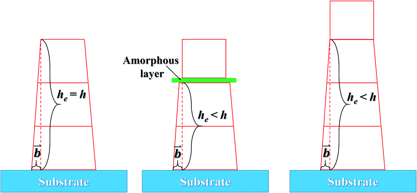 | ||
| Fig. 10 Schematic diagram illustrating the transmission of induced stress in thin films. | ||
However, even if the nanocrystals are in close contact, the substrate stress imposed on the nanocrystals of the composite thin films will decrease as the distance from the substrate increases. The substrate-induced interaction on the surface of the thin film is inevitably smaller than that in the bottom region where the thin film contacts the substrate. When the thin film is thicker than a critical threshold, the substrate-induced interaction is insufficient to make the nanocrystals on the top surface of the thin film grow along a certain orientation (Fig. 10). As the thickness of the thin film increases further, the region where the crystalline phase grows randomly expands, and the orientation degree of the whole thin film decreases as shown in Fig. 9.
It should be noted that the transfer of the substrate-induced interaction between the nanocrystals of one phase is usually hindered by the other phase in a bi-phased composite. However, as shown in Fig. 1 and 7, a good (100) orientation of NZFO can form well in the composite thin films with the ferrite mole fraction varying from 0.2 to 1.0. Particularly, when x ≥ 0.2, the substrate induction could already be transferred in the normal direction in the xBTO–(1−x)NZFO composite thin films. The NZFO lattices contact each other in the normal direction and a vertical NZFO percolation path comes into being.
More significantly, the presence of the vertical percolation path composed of the (100)-oriented NZFO nanocrystals surprisingly gives rise to a colossal magnetoelectric coupling effect in as-prepared BTO–NZFO composite thin films derived from 0–3 process. As shown in Fig. 11, the magnetization strength of the 0.6(random)BTO–0.4(100)NZFO composite thin film exhibits a significant mutation (>9%) at the Curie point of BTO (∼375 °C). This value approaches quite closely to that of the conventional double oriented 1–3 type thin films.12,13 Comparatively, no magnetoelectric coupling was observed in the composite thin films without any orientation. The plots of the lattice constants of BTO and NZFO in (1−x)BTO–xNZFO composite thin films in the presence and absence of the orientation of ferrite nanocrystals are also demonstrated in Fig. 12. While the lattice constants out-of-plane are calculated by Bragg equation based on the XRD data in normal direction, those in-plane are obtained from the XRD results measured by GID technology (Fig. S1†).25 As can be seen, although an obvious reduction can be observed for the BTO lattice in the composite thin films regardless of the orientation of ferrite nanocrystals at the Curie point of BTO (∼375 °C), only the NZFO lattice in oriented composite thin films can change to a considerable extent. It is noteworthy that the mutation of ferrite lattice disappears in pure NZFO thin film, which implies that the mutation of ferrite lattice is probably caused by the change of the BTO lattice.
 | ||
| Fig. 11 Magnetization strength curves of 0.6BTO–0.4NZFO composite thin films with and without (100)-orientation at different temperatures. | ||
 | ||
| Fig. 12 Lattice constants along out-of-plane and in-plane direction of BTO and NZFO in (1−x)BTO–xNZFO composite thin films with different ferrite contents and orientations. | ||
As per our previous research,17 a novel 1–3 structure, in which the ferromagnetic NZFO grains connect with one another to form percolation paths out-of-plane and the connection between them is blocked by the ferroelectric BTO grains, would come into being in the BTO–NZFO composite films at the thickness of 100 nm, when the NZFO content was controlled in the region of 0.3–0.5. On the other hand, as is known, when a ferroelectric reaches its Curie point, a ferroelectric phase transition will occur. The ferroelectric phase transition is a first order phase transition, which results in a change of lattice structure from cubic to tetragonal. The ferroelectric phase transition of BTO is an axial deformation from tetragonal to cubic structure. In 1–3 percolative composite thin films where BTO and NZFO percolate along normal direction, the axial deformation of BTO inevitably results in an axial stress on its neighboring NZFO nanocrystals, regardless of the orientation of BTO. If the NZFO nanocrystals take orientation, the axial stress from BTO will lead to the overall deformation of ferromagnetic NZFO lattice (Fig. 12(a)), or precisely, the value of c/a of the NZFO lattice is not equal to 1. By contrast, if the NZFO nanocrystals are randomly arranged, the deformation of different NZFO lattices is also random. The completely random deformation of different lattices will result in a uniform enlargement, reduction or invariability of the lattice overall, and the value of c/a is still equal to 1 (Fig. 13(b)). As is known, the easy axis of magnetization of the NZFO lattice with spinel structure always is along 〈111〉, while the magnetization is mainly decided by the angle between the easy axis and the magnetic moments.22 The change of lattice structure inevitably results in the change of the angle between the easy axis and the magnetic moments, and resultantly the magnetization. Therefore, when the ferromagnetic lattice in the multiferroic composite changes due to the stress caused by the deformed ferroelectric lattice, the magnetization of the composite would change accordingly; meanwhile, if the lattice structure of the ferromagnetic phase keeps unchanged, the magnetization would keep stable as well.12 More precisely, a remarkable magnetoelectric coupling appears in multiferroic system only when the lattice structures of both ferromagnetic and ferroelectric phases change.2 Thus, the results shown in Fig. 11 and 12 indicate that a much stronger magnetoelectric coupling occurs in the BTO–NZFO composite with (100)-oriented NZFO. In a word, the magnetoelectric coupling can actually be tailored by the orientation of the nanocrystals of only one component in a multiferroic composite.
 | ||
| Fig. 13 Schematic diagram depicting the stress and the strain of the lattice in thin films (a) with and (b) without orientation. | ||
Conclusions
In this work, a systematic study on the formation mechanism of oriented NZFO in the BTO–NZFO composite thin films prepared via a simple 0–3 composite fabrication process of magnetron sputtering is presented. An in-depth analysis revealed that the growth of the NZFO lattice along the (100) orientation can be attributed to the similarity between the ion distribution of the (111)-Si substrate and the (800) plane of NZFO nanocrystals as well as the transfer of the substrate stress between the closely contacted nanocrystals. When the sputtering power and sintering temperature were optimized as 200 W and 800 °C, respectively, the oxide layer on the (111) single-crystal silicon substrate could be completely removed, and the (100) orientation of NZFO reaches optimal state in the thin films. It is evident that strong magnetoelectric coupling exists in as-prepared multiferroic composite thin films with (100) oriented ferrite, and it can be controlled via the orientation of only one constituent phase. This contribution brings about new conception of developing high-performance multiferroic composite materials as well as realizing strong magnetoelectric coupling effect in such systems.Conflicts of interest
There are no conflicts to declare.Acknowledgements
This work is supported by the National Natural Science Foundation of China (Grant No. 51802345, 51701237 and 51772269).References
- M. Fiebig, T. Lottermoser, D. Meier and M. Trassin, The evolution of multiferroics, Nat. Rev. Mater., 2016, 1, 16046 CrossRef CAS.
- J. M. Hu, L. Q. Chen, C. W. Nan, J. M. Hu, L. Q. Chen and C. W. Nan, Multiferroic Heterostructures Integrating Ferroelectric and Magnetic Materials, Adv. Mater., 2016, 28, 15–39 CrossRef CAS PubMed.
- X. Yang, Z. Zhou, T. Nan, Y. Gao, G. M. Yang, M. Liu and N. X. Sun, Recent advances in multiferroic oxide heterostructures and devices, J. Mater. Chem. C, 2016, 4, 234–243 RSC.
- Z. Li, K. Tao, J. Ma, Z. P. Gao, V. Koval, C. J. Jiang, G. Viola, H. F. Zhang, A. Mahajan, J. Cao, M. Cain, I. Abrahams, C. Nan, C. L. Jia and H. X. Yan, Bi3.25La0.75Ti2.5Nb0.25(Fe0.5Co0.5)0.25O12, a single phase room temperature multiferroic, J. Mater. Chem. C, 2018, 6, 2733–2740 RSC.
- N. A. Hill, Why Are There so Few Magnetic Ferroelectrics?, J. Phys. Chem. B, 2000, 104, 6694–6709 CrossRef CAS.
- P. Martins, A. Larrea, R. Gonçalves, G. Botelho, E. V. Ramana, S. K. Mendiratta, V. Sebastian and S. Lanceros-Mendez, Novel Anisotropic Magnetoelectric Effect on δ-FeO(OH)/P(VDF-TrFE) Multiferroic Composites, ACS Appl. Mater. Interfaces, 2015, 7, 11224–11229 CrossRef CAS PubMed.
- J. Y. Chen, Z. H. Tang, Y. L. Bai and S. F. Zhao, Multiferroic and magnetoelectric properties of BiFeO3/Bi4Ti3O12 bilayer composite films, J. Alloys Compd., 2016, 675, 257–265 CrossRef CAS.
- I. Calisir and D. A. Hall, Chemical heterogeneity and approaches to its control in BiFeO3-BaTiO3 lead-free ferroelectrics, J. Mater. Chem. C, 2018, 6, 134–146 RSC.
- S. Z. Lu and X. D. Qi, RF magnetron co-sputtering growth and characterisation of multiferroic composite films of Ni0.5Zn0.5Fe2O4 + BiFeO3, J. Mater. Chem. C, 2016, 4, 8679–8686 RSC.
- Y. Wang, J. Hu, Y. Lin and C. W. Nan, Multiferroic magnetoelectric composite nanostructures, NPG Asia Mater., 2010, 2, 61–68 CrossRef.
- X. Y. Lu, B. Wang, Y. Zheng and E. Ryba, Coupling Interactionin 1-3-Type Multiferroic Composite Thin Films, Appl. Phys. Lett., 2007, 90, 133124 CrossRef.
- H. Zheng, J. Wang, S. E. Lofland, Z. Ma, L. M. Ardabili, T. Zhao, L. S. Riba, S. R. Shinde, S. B. Ogale, F. Bai, D. Viehland, Y. Jia, D. G. Schlom, M. Wuttig, A. Roytburd and R. Ramesh, Multiferroic BaTiO3-CoFe2O4 Nanostructures, Science, 2004, 303, 661–663 CrossRef CAS PubMed.
- X. L. Lu, Y. Kim, S. Goetze, X. G. Li, S. N. Dong, P. Werner, M. Alexe and D. Hesse, Magnetoelectric Coupling in Ordered Arrays of Multilayered Heteroepitaxial BaTiO3/CoFe2O4 Nanodots, Nano Lett., 2011, 11, 3202–3206 CrossRef CAS PubMed.
- L. L. Li, L. Lu, D. W. Zhang, R. Su, G. Yang, J. Y. Zhai and Y. D. Yang, Direct Observation of Magnetic Field Induced Ferroelectric Domain Evolution in Self-Assembled Quasi (0-3) BiFeO3–CoFe2O4 Thin Films, ACS Appl. Mater. Interfaces, 2016, 8, 442–448 CrossRef CAS PubMed.
- C. Grimaldi and I. Balberg, Tunneling and Nonuniversality in Continuum Percolation Systems, Phys. Rev. Lett., 2006, 96, 666026 CrossRef PubMed.
- M. Newman and R. M. Ziff, Efficient Monte Carlo Algorithm and High-Precision Results for Percolation, Phys. Rev. Lett., 2000, 85, 4104 CrossRef CAS PubMed.
- Y. Tang, R. X. Wang, Y. Zhang, S. Li and P. Y. Du, Anisotropy of Percolation Threshold of BaTiO3-Ni0.5Zn0.5Fe2O4 Composite Films, Sci. Rep., 2019, 9, 7855 CrossRef PubMed.
- G. H. Dong, Z. Y. Zhou, M. M. Guan, X. Xue, M. F. Chen, J. Ma, Z. Q. Hu, W. Ren, Z. G. Ye, C. W. Nan and M. Liu, Thermal Driven Giant Spin Dynamics at Three-Dimensional Heteroepitaxial Interface in Ni0.5Zn0.5Fe2O4/BaTiO3-Pillar Nanocomposites, ACS Nano, 2018, 12, 3751–3758 CrossRef CAS PubMed.
- P. L. Zhu, Q. Zheng and R. Sun, Magnetic and dielectric properties of Ni0.5Zn0.5Fe2O4/barium titanate (BaTiO3) ceramic composites prepared by an in situ sol-gel method, J. Mater. Sci.: Mater. Electron., 2015, 26, 9074–9080 CrossRef CAS.
- B. Xiao, Y. Tang, G. D. Ma, N. Ma and P. Y. Du, Relation between the microstructure and the electromagnetic properties of BaTiO3/Ni0.5Zn0.5Fe2O4 ceramic composite, Appl. Phys. A, 2015, 119, 1291–1300 CrossRef CAS.
- S. Banerjee, P. Hajra, A. Datta, A. Bhaumik, M. R. Mada, S. Bandyopadhyay and D. Chakravorty, Magnetodielectric effect in Ni0.5Zn0.5Fe2O4-BaTiO3 nanocomposites, Bull. Mater. Sci., 2014, 37, 497–504 CrossRef CAS.
- Y. Tang, Y. Zhang, G. D. Ma, N. Ma and P. Y. Du, Azimuthally Controlled Magnetic and Dielectric Properties of Multiferroic Nanocrystalline Composite by Magnetic Coupling and Charge Hopping, J. Phys. Chem. C, 2015, 119, 17995–18005 CrossRef CAS.
- R. J. D. Tilley, Crystals and Crystal Structures, John Wiley & Sons, Inc., England, 2006 Search PubMed.
- Y. Tang, Y. Zhang, Z. R. Wang, N. Ma and P. Y. Du, Control of Gradient Activation Energy on Formation and Properties of Multiferroic Composite Thin Film, J. Mater. Chem. C, 2016, 4, 2028–2039 RSC.
- Z. Zheng, T. Hu, Y. Y. Yao, W. J. Weng, G. R. Han, N. Ma and P. Y. Du, Strain-assisted control of high stable dielectric tunability in (1 0 0) oriented (Pb,Sr)TiO3 thin films, J. Alloys Compd., 2013, 576, 121 CrossRef CAS.
- Y. Tang, Y. Zhang, N. Ma and P. Y. Du, Control of the Nanostructure in Percolative Multiferroic Composites on the Dielectric Loss and Magnetism Threshold, J. Mater. Chem. C, 2015, 3, 9076–9088 RSC.
- Q. Y. Cai, M. Paulose, O. K. Varghese and C. A. Grimes, The effect of electrolyte composition on the fabrication of self-organized titanium oxide nanotube arrays by anodic oxidation, J. Mater. Res., 2005, 20, 230–236 CrossRef CAS.
- G. K. Mor, O. K. Varghese, M. Paulose and C. A. Grimes, Transparent Highly Ordered TiO2 Nanotube Arrays via Anodization of Titanium Thin Films, Adv. Funct. Mater., 2005, 15, 1291–1296 CrossRef CAS.
Footnote |
| † Electronic supplementary information (ESI) available. See DOI: 10.1039/c9ra03291f |
| This journal is © The Royal Society of Chemistry 2019 |