
 Open Access Article
 This Open Access Article is licensed under a
 Creative Commons Attribution 3.0 Unported Licence
Mott variable-range hopping transport in a MoS2 nanoflake†
Jianhong Xue a,
Shaoyun Huang*a,
Ji-Yin Wanga and
H. Q. Xu*abcd
a,
Shaoyun Huang*a,
Ji-Yin Wanga and
H. Q. Xu*abcd
aBeijing Key Laboratory of Quantum Devices, Key Laboratory for the Physics and Chemistry of Nanodevices, Department of Electronics, Peking University, Beijing 100871, China. E-mail: hqxu@pku.edu.cn; syhuang@pku.edu.cn
bBeijing Academy of Quantum Information Sciences, West Bld. #3, No. 10 Xibeiwang East Rd., Haidian District, Beijing 100193, China
cBeijing Academy of Quantum Information Sciences, Beijing 100193, China
dNanoLund, Division of Solid State Physics, Lund University, Box 118, S-221 00 Lund, Sweden
First published on 6th June 2019
Abstract
The transport characteristics of a disordered, multilayered MoS2 nanoflake in the insulator regime are studied by electrical and magnetotransport measurements. The MoS2 nanoflake is exfoliated from a bulk MoS2 crystal and the conductance G and magnetoresistance are measured in a four-probe setup over a wide range of temperatures. At high temperatures, we observe that ln![[thin space (1/6-em)]](https://www.rsc.org/images/entities/char_2009.gif) G exhibits a −T−1 temperature dependence and the transport in the nanoflake dominantly arises from thermal activation. At low temperatures, where the transport in the nanoflake dominantly takes place via variable-range hopping (VRH) processes, we observe that lnG exhibits a −T−1/3 temperature dependence, an evidence for the two-dimensional (2D) Mott VRH transport. Furthermore, we observe that the measured low-field magnetoresistance of the nanoflake in the insulator regime exhibits a quadratic magnetic field dependence ∼ αB2 with α ∼ T−1, fully consistent with the 2D Mott VRH transport in the nanoflake.
G exhibits a −T−1 temperature dependence and the transport in the nanoflake dominantly arises from thermal activation. At low temperatures, where the transport in the nanoflake dominantly takes place via variable-range hopping (VRH) processes, we observe that lnG exhibits a −T−1/3 temperature dependence, an evidence for the two-dimensional (2D) Mott VRH transport. Furthermore, we observe that the measured low-field magnetoresistance of the nanoflake in the insulator regime exhibits a quadratic magnetic field dependence ∼ αB2 with α ∼ T−1, fully consistent with the 2D Mott VRH transport in the nanoflake.
Despite the rapid developments in MoS2 layered materials and device applications, the nature of charge transport still remains elusive, since the experimentally measured carrier mobility in the materials is significantly lower than theoretical prediction.1–4 Disorders, such as sulphur vacancies, charge impurities, surface absorbents, charged traps at MoS2 layer–substrate interfaces,5–8 etc., strongly influence the transport properties of the layered MoS2 materials. Generally, in a disordered system,9 transport can be divided into two different regimes, separated by the mobility edge EC. Tuning the Fermi energy EF across the mobility edge causes a metal–insulator transition10–12 from extended to localized states or vice versa. In the insulating regime, where carriers are all frozen to localized states at energies below the mobility edge EC at zero temperature, carrier transport can take place via thermal activation at relatively high temperatures and via variable-range hopping (VRH) at low but finite temperatures. When the carrier transport is predominantly due to thermal activation, the conductance (G) exhibits a temperature (T) dependence of ln
G ∼ −T−1 and, thus, the characteristics activation energy Ea can be extracted from the Arrhenius plot of the measured conductance G as a function of temperature T. When temperature goes higher than a critical value (∼100 K in many compound semiconductor materials), phonon scattering can become significantly strong, leading to a characteristic temperature dependence that the conductance decreases with increasing temperature. At low temperatures, the current is carried via VRH processes in which a localized electron at the Fermi level moves to another localized state in an optimum hopping distance. The optimum distance is determined by the tradeoff between the lowest energy differences and the shortest hopping distances. In a noninteracting d-dimensional system, the density of states NF at the Fermi level is finite and the conductance can be well described by the Mott VRH mechanism13 with lnG ∼ −T−p where exponent p = 1/(d + 1). Pollak,14,15 Efros and Shklovskii16 pointed out that a soft gap can be opened up at the Fermi level by taking into account the long range electron–electron Coulomb interactions. The density of states at the Fermi level thus vanishes and the conductance should be described by the so called ES VRH mechanism17–19 with exponent p = 1/2 in lnG ∼ −T−p, independent of the dimension.
Due to the two-dimensional (2D) nature and the natural presence of disorders, layered MoS2 offers a renewed platform to investigate VRH mechanisms of 2D transport. Thermally activated transport,20 and nearest neighbor hopping (NNH) and VRH transport5–8,21–24 have been observed and discussed in many recent experimental studies of disorders, layered MoS2. Wu et al.,5 Ghatak et al.7 and Jariwala et al.8 studied the transport properties of atomically thin layer MoS2 devices and found that the transport in the MoS2 layers are well described by the 2D Mott VRH mechanism over a wide range of temperatures T (300–30 K). Qiu et al.6 examined the transport properties of few-layer MoS2 devices at low carrier densities and found that 2D Mott VRH mechanism dominate only the transport in the MoS2 layer in a low T region (100–20 K), while in the high T region (300–100 K) NNH dominates the transport in the layers. Liang et al.24 found a similar transition between NNH and VRH while the corresponding transition temperature is 70 K. Lo et al.21 studied transport in a monolayer MoS2 nanoflake and found that both the Mott and the ES VRH models can provide satisfactory explanation for their measurements at T < 190 K. Very recently, Kim et al.22 and Papadopoulos et al.23 studied transport in few-layered nanoflakes of n-butyllithium treated polymorphic MoS2. While Kim et al.22 found that their transport measurements are described by the 2D Mott VRH mechanism, Papadopoulos et al.23 showed contradictorily that the transport in their few-layered MoS2 nanoflakes is well described by the ES VRH mechanism. In all the above mentioned works, the temperature-dependent measurements of the conductance or the resistance are exclusively analyzed to determine transport mechanisms. Beside some controversies are present in assignment of VRH transport mechanisms, no carrier density dependent transition between different transport mechanisms was reported in these works.
Magnetotransport measurements could also be used to distinguish the two VRH mechanisms in the disordered MoS2 layers. In a common situation where the magnetoresistance shows a quadratic dependence on magnetic field as αB2, the coefficient α has different temperature dependences for the two VRH transport mechanisms.25 In the Mott VRH regime the coefficient α ∝ T−3/(d+1), whereas in the ES VRH regime the coefficient α ∝ T−3/2. Thus, magnetotransport measurements could be analyzed together with the temperature and carrier density dependent measurements to identify the transport mechanisms in disordered MoS2 nanoflakes. We notice that although there are some works26 reporting the magnetoresistance of MoS2, no efforts to distinguish between the Mott and ES VRH transports based on magnetotransport measurements has been made yet.
In this work, we report on an experimental study of the transport characteristics of a disordered MoS2 nanoflake by electrical and magnetotransport measurements in a four-probe setup over a temperature range of 6 to 300 K and at different carrier densities. The study is focused on the insulator regime where the Fermi energy EF lies below the mobility edge EC. When EF is tuned close to EC, the characteristics of thermally activated transport and phonon scattering are observed in the conductance measurements of the nanoflake. When EF is tuned far below EC, the measured lnG shows a −T−1 dependence at relatively high temperatures and a −T−1/3 dependence at relatively low temperatures. A good quadratics magnetic field dependence ∼ αB2 of the magnetoresistance is also observed in the nanoflake and a T−1 dependence of coefficient α is extracted. These electrical and magnetotransport measurements provide a solid evidence that the Mott VRH rather than ES VRH transport is the dominant transport mechanism in our disordered MoS2 nanoflake in the insulating regime at low temperatures.
The MoS2 nanoflakes studied in this work are obtained by exfoliation from a commercially available bulk MoS2 crystal. The exfoliated MoS2 nanoflakes are transferred onto a highly doped silicon substrate covered with a 300 nm-thick layer of SiO2 on top. Electrical contacts are prepared using electron-beam lithography (EBL) for pattern definition, electron-beam evaporation for deposition of 5 nm-thick titanium and 50 nm-thick gold, and lift-off process. Fig. 1(a) shows an atomic force microscope (AFM) image of a fabricated device measured for this work and the schematic for the measurement circuit setup. The MoS2 nanoflake in the device has a width of W ∼ 400 nm and a thickness of t ∼ 10 nm, see the AFM line scan measurements across an edge of the nanoflake shown in the lower panel of Fig. 1(a). The device consists of four metal stripe contacts, which we labeled as contacts 1 to 4 as in Fig. 1(a). These contacts have a width of 200 nm. The edge-to-edge distances between contacts 1 and 2, between contacts 2 and 3, and between contacts 3 and 4 are 80, 450 and 100 nm, respectively. The measurements are performed in a Physical Property Measurement System (PPMS) cryostat, which provides temperatures in a range of 300 to 2 K and magnetic fields up to 9 Tesla. The four-probe setup is adopted in the measurements, in order to exclude the contact resistances, in which a source–drain bias voltage Vds is applied between contacts 1 and 4, the channel current Ids and the voltage drop (V23) between contacts 2 and 3 are simultaneously recorded, see the circuit setup in Fig. 1(a). The Fermi level EF in the nanoflake is modulated by a voltage Vg applied to the silicon substrate (back gate).
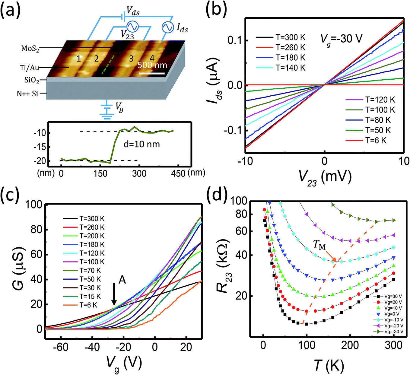 | ||
| Fig. 1 (a) AFM image of the MoS2 nanoflake device and schematic view of the device layer structure and measurement setup (top panel), and height profile measured using AFM along the dashed line in the AFM image (bottom panel). Here it is shown that the MoS2 nanoflake in the device has a thickness of 10 nm. (b) Source–drain current Ids vs. voltage V23 measured for the device at temperatures from 6 to 300 K and at back gate voltage Vg = −30 V. (c) Transfer characteristics of the field-effect device at temperatures from 6 to 300 K. (d) Resistance of the nanoflake plotted against temperature T at different back gate voltages. TM marks the temperature position at which the resistance has a minimum in the curve measured at each back gate voltage. The dashed line connecting the values of TM at different back gate voltages is the guide to the eyes. | ||
Fig. 1(b) shows the measured channel current Ids as a function of the voltage drop V23 between contacts 2 and 3 for the device shown in Fig. 1(a) at a fixed back gate voltage of Vg = −30 V and different temperatures. It is seen in the figure that the measured Ids–V23 curves are straight lines. The good linearity is found in all the measured Ids–V23 curves over a wide range of back gate voltages and of temperatures, which ensures that the transport characteristics of the MoS2 channel are extracted from the measurements. Fig. 1(c) shows the measured channel conductance G = Ids/V23 as a function of back gate voltage Vg at different temperatures. It is seen that the device is a typical n-type transistor. The channel conductance shows very different temperature dependence at high back gate voltages (on the right side of point A) and at low back gate voltages (on the left side of point A), where the crossover point A is located at Vg ∼ −30 V, as indicated by a black arrow in Fig. 1(c). At the high back gate voltages (on the right side of point A), the conductance G is increased with decreasing temperature and then becomes decreased with further lowering temperature. At the low back gate voltages (on the left side of point A), however, the conductance G is monotonously decreased with decreasing temperature in the entire measured temperature range (from 300 to 6 K). The observed temperature dependence of the conductance at low temperatures indicates that the MoS2 channel is in the insulating regime and the Fermi energy EF lies below the mobility edge EC throughout the entire measurement range of back gate voltages. The characteristic conductance increase with decreasing temperature observed at high back gate voltages and high temperatures arises from the interplay between the thermal activation transport and phonon scattering. This interplay phenomena could be better visualized by plotting the resistance R23 as a function of temperature measured at different back gate voltages as shown in Fig. 1(d). Here, we can clearly recognize that at a given high back gate voltage Vg > −30 V, there exists a characteristic temperature TM, at which the resistance has a minimum. Apparently, TM increases with decreasing back gate voltage, see the yellow dashed line in Fig. 1(d), and can reach a temperature as low as ∼100 K at Vg = 30 V. Physically, at such a high back gate voltage, the Fermi level EF is close to the mobility edge EC and a significant number of carriers can be excited to the extended states located at energies above the mobility edge at high temperatures. Thus, at T > TM, the observed fact that the resistance decreases with decreasing temperature is mainly due to reduction in phonon scattering with decreasing temperature. However, at T < TM, the phonon scattering becomes less important and the resistance becomes closely related to the number of carriers which are thermally excited to the extended states. As the back gate voltage Vg decreases, the Fermi level EF is gradually moved away from the mobility edge EC, leading to an increase in TM as seen in Fig. 1(d).
Fig. 2 shows the Arrhenius plot of the measured conductance as a function of temperature at different back gate voltages. In the temperature region of 80 K < T < TM, i.e., the shaded part except for the upper-left corner region in the figure, relatively large thermal kinetic energy assisted transport dominates and the temperature dependence of the conductance can be well modelled by the thermally activated transport20 as Ga = G0e−Ea/kBT. Here, G0 is the conductance at the high temperature limit, Ea = (EC − EF) is the activation energy, and kB is the Boltzmann constant. The extracted activation energy Ea is shown in the inset of Fig. 2 as a function of the back gate voltage. The activation energy Ea decreases linearly with increasing Vg from −70 to −30 V and turns to saturate with further increasing Vg to the positive side, in good agreement with the fact that the Fermi level moves closer to the mobility edge with increasing back gate voltage.
 | ||
| Fig. 2 lnG plotted against T−1 (inverse of temperature) for the device at different back gate voltages. The region on the left marked by grey color is for the measurements at temperatures higher than ∼80 K, at which the transport in the nanoflake is well described by the thermal activation mechanism. The upper-left corner marked by light purple color is the region of the measurements at high temperatures and high positive gate voltages, where the characteristics of phonon scattering in the layered MoS2 is observed. Lines in the grey colored region are straight line fits to the measured data. The inset shows the extracted activation energy Ea from the straight line fits in the grey color region as a function of back gate voltage Vg. The red dashed line in the inset is a guide to the eyes to clarify the change of Ea. | ||
However, the thermally activated transport model does not describe the measurements in the low temperature region [the right, unshaded part of Fig. 2] as seen from the deviations from the fitting lines in the region. Physically, in this low temperature region, VRH conduction becomes dominant and is responsible for the temperature dependent characteristics of the measured conductance. In theory, the conductance in VRH mechanisms can be described as
 | (1) |
 | ||
| Fig. 3 (a) lnG plotted against T−1/2 for the device measured at different back gate voltages. Lines are straight line (2D ES VRH theory) fits to the measurement data at low temperatures. Clearly, the straight line fits do not describe the measurement data at temperatures of 25 to 80 K. (b) The same as in (a) but plotted against T−1/3. Lines are straight line (2D Mott VRH theory) fits to the measurement data at temperatures of 6 to 80 K. Here, excellent fits are obtained over this range of temperatures. The inset shows the extracted characteristic temperature T1/3 and localization length ξloc as a function of back gate voltage Vg for the MoS2 nanoflake based on the 2D Mott VRH theory. | ||
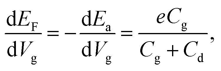
Employing the 2D Mott VRH mechanism, we can further analyze the temperature dependence of the conductance to extract the characteristic temperature T1/3 and localization length ξloc in the nanoflake at different gate voltages Vg. The results are shown in the inset of Fig. 3(b). It is seen that T1/3 monotonically decreases from ∼105 to ∼102 K with increasing Vg from −70 to 5 V. Theoretically, T1/3 is related to the localization length as T1/3 = 13.8/(kBNFξloc2), where NF is the density of states at Fermi level. The NF can be determined from the gate voltage dependence of the activation energy Ea by taking into account the quantum capacitance Cd as12,27
 | (2) |
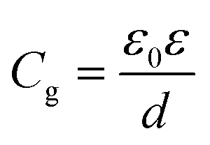 with ε0 being the vacuum permittivity, ε and d being the dielectric constant and layer thickness of SiO2. The calculated values of Cd and NF are from 6 to 10 μF cm−2 and from 3.75 to 6.25 × 10¹³ eV−1 cm−2, respectively. Thus, the derived localization length of the nanoflake is found to increase from 3.4 to 33.7 nm with increasing Vg from −70 to 5 V, as shown in the inset of Fig. 3(b).
Fig. 4(a) show the magnetoresistance characteristics at different temperatures in the 2D VRH transport regime at Vg = −20 V with the magnetic field B applied perpendicular to the MoS2 nanoflake. Here, the MoS2 nanoflake is in the x–y plane, the current flow is along the x axial direction, and the magnetoresistance is defined as ΔR23 = [R(B) − R(B = 0)]/R(B = 0). Clearly, the magnetoresistance shows a positive quadratic dependence on magnetic field B at temperatures below ∼50 K. In the wave-function shrinkage model,28–31 the positive quadratic magnetoresistance is attributed to the contraction of the electronic wave function at traps in a magnetic field, thus leading to a reduction of hopping probability. Quantitatively, in the wave-function shrinkage model, the magnetoresistance in the Mott VRH regime can be expressed as25
 | (3) |
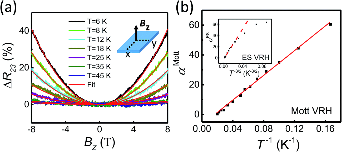 | ||
| Fig. 4 (a) Magnetoresistance as a function of magnetic field Bz applied perpendicular to the MoS2 nanoflake plane (as shown in the inset) measured at back gate voltage Vg = −20 V and at different temperatures. Red solid lines are fits to the measured data based on the wave-function shrinkage model. (b) Prefactor αMott as a function of T−1 extracted from the measured magnetoresistance curves at different temperatures T. The red solid line presents the predicted values of αMott by the wave-function shrinkage model in the Mott VRH regime. The inset shows the prefactor αES extracted from the same magnetoresistance measurements as a function of T−3/2. The dashed line in the inset shows the results that would be predicted by the wave-function shrinkage model in the ES VRH regime. | ||
In conclusion, the transport characteristics of a disordered MoS2 nanoflake have been investigated in details over a wide range of temperatures in the insulator regime, where the Fermi level EF in the nanoflake is tuned with use of the back gate voltage to lie below the mobility edge EC. At relatively high temperatures, the nanoflake exhibits activation transport characteristics. The activation energy Ea = EC − EF, which measures the energy distance between the mobility edge EC and the Fermi energy EF, is extracted in the nanoflake. It is found that the activation energy Ea decreases with increasing back gate voltage at low back gate voltages and turn to saturate towards zero at high back gate voltages. At sufficiently low temperatures, the transport characteristics of the nanoflake are found to be governed by VRH processes. To identify whether the Mott or the ES VRH mechanism plays a dominant role in the system at this low temperature region, the temperature dependent conductance and magnetoresistance have been measured and analyzed. It is found that in this low temperature region the lnG shows a −T−1/3 temperature dependence and the prefactor in the quadratic magnetic field dependent magnetoresistance scales with temperature as T−1. These results provide exclusive evidences that the 2D Mott VRH transport is the dominant transport mechanism at low temperatures in the insulating regime of our disordered MoS2 nanoflake.
Conflicts of interest
There are no conflicts of interest to declare.Acknowledgements
This work is supported by the Ministry of Science and Technology of China through the National Key Research and Development Program of China (Grant No. 2017YFA0303304, 2016YFA0300601, 2017YFA0204901, and 2016YFA0300802), the National Natural Science Foundation of China (Grant No. 11874071, 91221202, 91421303, and 11274021), and the Beijing Academy of Quantum Information Sciences (Grant No. Y18G22). HQX also acknowledges financial support from the Swedish Research Council (VR).References
- B. Radisavljevic, A. Radenovic, J. Brivio, V. Giacometti and A. Kis, Nat. Nanotechnol., 2011, 6, 147 CrossRef CAS PubMed.
- Q. H. Wang, K. Kalantar-Zadeh, A. Kis, J. N. Coleman and M. S. Strano, Nat. Nanotechnol., 2012, 7, 699 CrossRef CAS PubMed.
- Z. Yu, Z.-Y. Ong, S. Li, J.-B. Xu, G. Zhang, Y.-W. Zhang, Y. Shi and X. Wang, Adv. Funct. Mater., 2017, 27, 1604093 CrossRef.
- K. Kaasbjerg, K. S. Thygesen and K. W. Jacobsen, Phys. Rev. B: Condens. Matter Mater. Phys., 2012, 85, 115317 CrossRef.
- J. Wu, H. Schmidt, K. K. Amara, X. Xu, G. Eda and B. Ozyilmaz, Nano Lett., 2014, 14, 2730 CrossRef CAS PubMed.
- H. Qiu, T. Xu, Z. Wang, W. Ren, H. Nan, Z. Ni, Q. Chen, S. Yuan, F. Miao, F. Song, G. Long, Y. Shi, L. Sun, J. Wang and X. Wang, Nat. Commun., 2013, 4, 2642 CrossRef PubMed.
- S. Ghatak, A. N. Pal and A. Ghosh, ACS Nano, 2011, 5, 7707 CrossRef CAS PubMed.
- D. Jariwala, V. K. Sangwan, D. J. Late, J. E. Johns, V. P. Dravid, T. J. Marks, L. J. Lauhon and M. C. Hersam, Appl. Phys. Lett., 2013, 102, 173107 CrossRef.
- N. Mott, M. Pepper, S. Pollitt, R. H. Wallis and C. J. Adkins, Proc. R. Soc. London, Ser. A, 1975, 345, 169 CrossRef CAS.
- B. Radisavljevic and A. Kis, Nat. Mater., 2013, 12, 815 CrossRef CAS PubMed.
- B. W. Baugher, H. O. Churchill, Y. Yang and P. Jarillo-Herrero, Nano Lett., 2013, 13, 4212 CrossRef CAS PubMed.
- D. Ovchinnikov, A. Allain, Y. S. Huang, D. Dumcenco and A. Kis, ACS Nano, 2014, 8, 8174 CrossRef CAS PubMed.
- N. F. Mott, J. Non-Cryst. Solids, 1968, 1, 1 CrossRef CAS.
- M. Pollak, Discuss. Faraday Soc., 1971, 1970, 13 Search PubMed.
- M. L. Knotek and M. Pollak, J. Non-Cryst. Solids, 1972, 8, 505 CrossRef.
- A. L. Efros and B. I. Shklovskii, J. Phys. C: Solid State Phys., 1975, 8, L49 CrossRef CAS.
- S. I. Khondaker, I. S. Shlimak, J. T. Nicholls, M. Pepper and D. A. Ritchie, Solid State Commun., 1999, 109, 751 CrossRef CAS.
- Y. Zhang, P. Dai, M. Levy and M. P. Sarachik, Phys. Rev. Lett., 1990, 64, 2687 CrossRef CAS PubMed.
- A. Aharony, Y. Zhang and M. P. Sarachik, Phys. Rev. Lett., 1992, 68, 3900 CrossRef CAS PubMed.
- A. Ayari, E. Cobas, O. Ogundadegbe and M. S. Fuhrer, J. Appl. Phys., 2007, 101, 014507 CrossRef.
- S. T. Lo, O. Klochan, C. H. Liu, W. H. Wang, A. R. Hamilton and C. T. Liang, Nanotechnology, 2014, 25, 375201 CrossRef PubMed.
- J. S. Kim, J. Kim, J. Zhao, S. Kim, J. H. Lee, Y. Jin, H. Choi, B. H. Moon, J. J. Bae, Y. H. Lee and S. C. Lim, ACS Nano, 2016, 10, 7500 CrossRef CAS PubMed.
- N. Papadopoulos, G. A. Steele and H. S. J. van der Zant, Phys. Rev. B, 2017, 96, 235436 CrossRef.
- S. Liang, H. Yang, P. Renucci, B. Tao, P. Laczkowski, S. Mc-Murtry, G. Wang, X. Marie, J. M. George, S. Petit-Watelot, A. Djeffal, S. Mangin, H. Jaffres and Y. Lu, Electrical spin injection and detection in molybdenum disulfide multilayer channel, Nat. Commun., 2017, 8, 14947 CrossRef CAS PubMed.
- T.-I. Su, C.-R. Wang, S.-T. Lin and R. Rosenbaum, Phys. Rev. B: Condens. Matter Mater. Phys., 2002, 66, 054438 CrossRef.
- T.-E. Park, J. Suh, D. Seo, J. Park, D.-Y. Lin, Y.-S. Huang, H.-J. Choi, J. Wu, C. Jang and J. Chang, Appl. Phys. Lett., 2015, 107, 223107 CrossRef.
- W. Zhu, T. Low, Y.-H. Lee, H. Wang, D. B. Farmer, J. Kong, F. Xia and P. Avouris, Nat. Commun., 2014, 5, 3087 CrossRef PubMed.
- F. L. Bloom, W. Wagemans, M. Kemerink and B. Koopmans, Phys. Rev. Lett., 2007, 99, 257201 CrossRef CAS PubMed.
- Y.-B. Zhou, B.-H. Han, Z.-M. Liao, H.-C. Wu and D.-P. Yu, Appl. Phys. Lett., 2011, 98, 222502 CrossRef.
- R. Sadu, N. Haldolaarachchige, D. Chen and D. P. Young, Appl. Phys. Lett., 2013, 102, 212403 CrossRef.
- Y. Zhang, H. Ning, Y. Li, Y. Liu and J. Wang, Appl. Phys. Lett., 2016, 108, 153114 CrossRef.
Footnote |
| † Electronic supplementary information (ESI) available. See DOI: 10.1039/c9ra03150b |
| This journal is © The Royal Society of Chemistry 2019 |