
 Open Access Article
 This Open Access Article is licensed under a Creative Commons Attribution-Non Commercial 3.0 Unported Licence
Electronic and optical absorption properties of organic–inorganic perovskites as influenced by different long-chain diamine molecules: first-principles calculations†
Wangzhe Zhou,
Dan Li *,
Di Zhang,
Hu Tang,
He Zhang and
Chunjun Liang*
*,
Di Zhang,
Hu Tang,
He Zhang and
Chunjun Liang*
Department of Physics, Beijing Jiaotong University, Beijing 1001044, People's Republic of China. E-mail: danli@bjtu.edu.cn; chjliang@bjtu.edu.cn
First published on 13th May 2019
Abstract
Organic–inorganic perovskites have demonstrated significant promise as photovoltaic materials due to their excellent photoelectric properties. However, monoamino three-dimensional (3D) perovskites, such as CH3NH3PbI3 (MAPbI3) and NH2CHNH2PbI3 (FAPbI3) exhibit low thermal and chemical stability, leading to low device durability. As such, we sought to address this problem by evaluating the performance of five diamino-3D perovskites with different molecule chain lengths, including NH3(CH2)2NH3PbI4 (EDAPbI4), NH3(CH2)3NH3PbI4 (DPAPbI4), NH3(CH2)4NH3PbI4 (BDAPbI4), NH3(CH2)5NH3PbI4 (PDAPbI4), and NH3(CH2)6NH3PbI4 (HDAPbI4), as well as one monoamino-2D perovskite, (CH3(CH2)3NH3)2PbI4 (BA2PbI4) using first-principles calculations. We analyzed the geometries, formation energies, electronic structures, and optical absorption properties of each of these materials. We determined the composition of the conduction and valence bands and analyzed the charge transfer between the inorganic layer and organic molecules. The transport characteristics of the electrons in the different directions were analyzed by calculating the effective mass in different directions. Based on these results, BDAPbI4 was predicted to exhibit the best photovoltaic performance, as well as demonstrating a light effective mass of the electrons and holes, a reduced bandgap, and a large optical absorption, compared to the other perovskites assessed in this study.
1. Introduction
Since the development of organic–inorganic halide perovskite solar cells in 2009,1 their importance in the field of solar power research has increased substantially. After several years of development, these solar cells have demonstrated many advantages, including an appropriate bandgap, high absorption coefficient, high carrier mobility, and low carrier recombination rate.2 The power conversion efficiency of 3D perovskites has rapidly reached 23.7%,3 showing great commercial potential. However, 3D perovskites have issues with low luminescence activity and low stability regarding heat and moisture.4,5 Generally, the structure of 3D perovskites consists of PbX3 (X = Cl, Br, and I) as the skeleton and methylamine (MA) at the center of the structure. With this structure, internal factors such as ion migration, electron transfer, and interfacial reaction6–8 as well as external factors such as humidity and oxidant9,10 can have important effects on its stability. For example, in Schoonman et al., the Pb–I bond component in organic–inorganic hybridized methylammonium lead-halide perovskite can lead to photolysis.11 Therefore, researchers have introduced the use of 2D perovskites to solve such problems.12–15 The existence of the organic layer enhances the stability of the compound to heat and moisture,16–21 but it also leads to a high bandgap, with the bandgap for (CH3(CH2)3NH3)2PbI4 and (CH3(CH2)3NH3)2(CH3NH3)Pb2I7 calculated by Stoumpos et al. being 2.43 eV and 2.17 eV, respectively,17 less optical absorption, low interlayer mobility of carriers,18,19 and reduced energy conversion efficiency,19,20 which limits the application of 2D perovskite materials in photovoltaic harvesters.In this paper, we use diamino groups as organic substances to form 3D perovskites. Considering the instability of short-chain molecules, such as methylamine (MA) and formamidine (FA), we have introduced long-chain molecules, including 1,3-diaminopropane (DPA), 1,4-butanediamine (BDA), and 1,5-pentanediamine (PDA). We investigated whether these diamino-3D perovskites had increased stability, in an effort to address the instability problem of organic–inorganic halide perovskites, and if they could maintain the excellent characteristics of perovskites, such as their low loss, high carrier mobility, and large optical absorption. In order to compare the diamino-3D perovskites, we also produced a 2D perovskite whose organic molecules consisted of monoamino butylamine (BA), with the amino groups of the two BA molecules attracted to the inorganic layer and the other end serving as a vacuum layer. We studied the geometries, formation energies, electronic structures, and optical absorption properties of monoamino-2D perovskite (BA2PbI4) and the diamino-3D perovskites (EDAPbI4, DPAPbI4, BDAPbI4, PDAPbI4, and HDAPbI4) using the first-principles method based on density functional theory (DFT). This study will help in the design and synthesis of more efficient and stable organic–inorganic perovskite optoelectronic devices.
2. Computational methodology
The first-principles calculations were performed using the Vienna Ab initio Simulation Package (VASP),22 the electron–ion interaction was described using the projection-enhanced plane wave (PAW) pseudopotential,23 and the Perdew–Burke–Ernzerhof (PBE) of generalized gradient approximation (GGA) was used to describe the exchange–correlation energy between the electrons.24 Electronic orbitals 5d6s6p, 5s5p, 2s2p, 2s2p, and 1s were considered in valence for Pb, I, C, N, and H atoms, respectively. The cut-off energy for the plane wave basis set was 500 eV. The convergence criterion of the self-consistent calculations for ionic relaxations was 10−5 eV between two consecutive steps. The first Brillouin zone was sampled using a gamma-centered method to generate k-point meshes. In the structural optimization, the K-point grid size for BA2PbI4 was 4 × 4 × 1, as it had a vacuum layer in the c direction; the K-point grid size for diamino-3D perovskites was 4 × 4 × 4. In order to acquire a more accurate wave function and charge density, 16 × 16 × 1 and 16 × 16 × 16 k-point grids were used in the static calculation. Considering the influence of intermolecular forces on the calculation results, a van der Waals correction was performed via the zero damping DFT-D3 method of Grimme in VASP.25 The charge densities of the VBM states and CBM states on each atom were integrated using Bader analysis.26–28The band structure calculation of MAPbI3 using the PBE exchange–correlation functional of GGA shows the well-known weakness of band gap underestimation is not found, GGA band gaps are very similar with the experimental values.29 It is generally believed that this accidental agreement is from the error cancelation, i.e., neglecting the spin–orbit interaction caused band gap overestimation, which cancels the underestimation error of GGA calculation.30 The strong SOC effect results in a very large splitting of the CBM states, the underestimated band gap is corrected by HSE06 functional or GW self-energy approach incorporating SOC. For example, the band gaps of BA2PbI4 and MAPbI3 calculated by Biao Liu et al. using HSE + SOC functional calculation are about 0.1 eV lower than PBE.31 SOC–GW delivers calculated band gaps 1.67 eV for MAPbI3 in excellent agreement with the experimental values.32 But SOC has a very small effect on the atomic structure and ground-state properties.33 Therefore, we adopt the PBE exchange–correlation as a practical choice to reflect the real band gap.
3. Results and discussion
3.1 Geometric structure and formation energy
The optimized structures of BA2PbI4, DPAPbI4, BDA2PbI4, and PDAPbI4 with minimum energy after ion relaxation are shown in Fig. 1. The optimized structures of EDAPbI4 and HDAPbI4 are shown in Fig. S1.† The amino group (BA) is positively charged and adsorbs with the negatively charged Pb–I inorganic layer. Therefore, we use a structure in which two single amino groups (BA) are adsorbed by an inorganic layer to form 2D perovskite (BA2PbI4), and a structure in which a double amino group and upper and lower inorganic layers are used to form 3D perovskites (EDAPbI4, DPAPbI4, BDAPbI4, PDAPbI4, and HDAPbI4). As shown in Fig. 1(c) and (d), it can be seen that with the increased length of the main chain of the diamino molecule in the 3D perovskite, the molecular chain is bent, which may have been caused by the soft skeleton of the long chain molecule. Because long-chain diamino molecules interact with the upper and lower inorganic layers, the supercell deviates from the orthogonal symmetry and degenerates into triclinic symmetry. The degree of supercell tilt is characterized by the value of |Δα| + |Δβ| + |Δγ|. Here, Δα, Δβ, and Δγ are the differences in the angle between the base vectors and the 90 degree angle, respectively. From the data presented in Table 1, among the five kinds of diamino-3D perovskites, the values of |Δα| + |Δβ| + |Δγ| for EDAPbI4, BDAPbI4, and HDAPbI4 are relatively small, at 6.9, 13.9, and 15.3 degrees, respectively. However, the values of |Δα| + |Δβ| + |Δγ| for DPAPbI4 and PDAPbI4 are 17.3 and 24.6 degrees, respectively, which are relatively large. It was found that the perovskite structure had a higher symmetry when the number of atoms in the main chain of the diamino molecules was even. For example, in EDAPbI4, BDAPbI4, and HDAPbI4 there are two N atoms and two, four, and six C atoms in the main chain of the diamino molecule, respectively. When the number of atoms in the main chain was even, the molecule had an inversion symmetry. It was observed that the inversion symmetry molecules in the inorganic skeleton generally did not rotate along the axis, but they only bent with the increase of the length of the molecular chain, as shown in Fig. 1(c), S1(a) and (b).† It was shown that the deformation of the inorganic skeleton formed by Pb and I was relatively small, leading to a smaller deviation from the orthogonal symmetry. In contrast, when the number of atoms in the main chain was odd, the molecules did not demonstrate inversion symmetry but had a mirror symmetry instead, such as DPAPbI4 and PDAPbI4, which have two N atoms as well as three and five C atoms in the main chain of the diamino molecule, respectively. It was found that the molecules without inversion symmetry rotate along the axis in order to maintain the inversion symmetry of the inorganic skeleton; correspondingly, the inorganic Pb–I layers are also obviously distorted, as shown in Fig. 1(b) and (d). In addition, it is important to note that the bandgap and band structure depends on the symmetry of the crystal, which is discussed below. Obviously, the lattice constant c increased with the increase in molecular chain length, from the lattice constant c of 9.40 Å for EDAPbI4 to that of 12.91 Å for HDAPbI4 (Table 1). In (BA)2PbI4, a monolayer 2D perovskite was formed by monoamino molecular ions as organic layers. Because two long chain monoamino ions (BA) interact with only one inorganic Pb–I4 layer, the geometric structure of the atoms in the plane of the Pb–I4 layer was greatly affected, resulting in a larger deviation of the γ angle from a right angle, while the α and β angles were basically right angles (Table 1). | ||
| Fig. 1 The optimized geometrical structures of (a) BA2PbI4, (b) DPAPbI4, (c) BDAPbI4, and (d) PDAPbI4 perovskites. The purple, gray, brown, silver, and smallest balls represent I, Pb, C, N, and H atoms, respectively. The red number is the length of the corresponding Pb–I bond in angstroms. | ||
| Compounds | a | b | c | α | β | γ | |Δα| + |Δβ| + |Δγ| | I–I | Ef | Eg |
|---|---|---|---|---|---|---|---|---|---|---|
| (BA)2PbI4 | 6.35 | 6.06 | — | 91.6 | 89.4 | 98.1 | 10.3 | — | 0.37 | 2.49 |
| EDAPbI4 | 6.42 | 6.04 | 9.40 | 89.6 | 96.3 | 90.2 | 6.9 | 3.97 | 0.49 | 2.30 |
| DPAPbI4 | 6.06 | 6.25 | 10.20 | 83.5 | 87.0 | 97.7 | 17.3 | 3.83 | 0.26 | 2.22 |
| BDAPbI4 | 6.29 | 6.23 | 10.61 | 82.7 | 94.9 | 88.3 | 13.9 | 4.25 | 0.29 | 1.78 |
| PDAPbI4 | 6.24 | 6.28 | 11.52 | 78.9 | 82.5 | 84.1 | 24.6 | 5.21 | −0.01 | 2.18 |
| HDAPbI4 | 6.36 | 6.12 | 12.91 | 89.7 | 103.7 | 91.3 | 15.3 | 6.42 | 0.05 | 2.03 |
The following formulas were used to calculate the formation energy (Ef) of the monoamine-2D perovskite and diamino-3D perovskites:
| Ef[(BA)2PbI4] = E[(BA)2PbI4] − E(PbI2) − 2E(BAI) | (1) |
| Ef[DPbI4] = E[DPbI4] − E(PbI2) − E[DI2] | (2) |
The calculated formation energies of the 2D perovskite (BA2PbI4) and 3D perovskites (EDAPbI4, DPAPbI4, BDAPbI4, PDAPbI4, and HDAPbI4) were 0.37, 0.49, 0.26, 0.29, −0.01, and 0.05 eV, respectively (see Table 1). The positive formation energies indicated that the synthesis reaction was an endothermic reaction, and the negative formation energies show that the reactions were exothermic. There is no doubt that PDAPbI4 is the easiest to synthesize. In general, the formation energy of perovskite materials formed by diamino molecules with longer main chains was relatively low (Table 1). The reason may be that the skeleton of long chain molecules is softer and easier to deform, resulting in lower formation energy. In addition, because the Pb–I inorganic layer is negatively charged, electrostatic repulsion occurs between two adjacent layers. When the length of the chain becomes longer, the inorganic layer spacing increases. The electrostatic attraction energy between the amino group and the inorganic layer remained basically unchanged, and the reduction of the electrostatic repulsion energy also resulted in the reduction of the formation energy. Moreover, the formation energy of the diamino-3D DPAPbI4 perovskite was lower than that of the monoamino-2D BA2PbI4 perovskite, although they have the same main chain length. In order to compare with the formation energy of traditional perovskite (MAPbI3 and FAPbI3), we also calculated the formation energy of per primitive for pseudo-cubic MAPbI3 and FAPbI3, which are 0.08 and −0.04 eV, respectively, close to the formation energies of PDAPbI4 and HDAPbI4 with long chain diamino molecules. Although the negative and significantly low formation energies indicate that PDAPbI4 and HDAPbI4 are easier synthesize in experiments, appropriate large formation energy can enhance the stability of 2D and 3D perovskite.34
3.2 Electronic properties
The calculated energy band structures of BA2PbI4, DPAPbI4, BDA2PbI4, and PDAPbI4 are shown in the middle of Fig. 2. The energy band structures of EDAPbI4 and HDAPbI4 are shown in Fig. S2.† The upper left corner of Fig. 2 is the Brillouin zone of the 2D and 3D perovskites, respectively. The 2D material has a vacuum layer in the c direction, so its Brillouin zone is also 2D. In order to take as many high symmetry points in the Brillouin zone as possible, we selected G, X, L1, G, Y, L1, G, L2, X, G paths and N, R, X, L, R, Y, M, R, G, Z, R paths to the perform the band calculations. We found that for 2D perovskite BA2PbI4 the valence band maximum (VBM) appeared at the L1 and L2 points, but the conduction band minimum (CBM) appeared at K points near L1 and L2 with a certain offset, which indicated that BA2PbI4 was an indirect bandgap semiconductor with a bandgap of 2.49 eV. It is interesting to note that the bandgap and band structure depended on the symmetry of the crystal. In EDAPbI4, BDAPbI4, and HDAPbI4 there are an even number of atoms in the main chain of the diamino molecules, which generate similar inversion symmetries, resulting in similar band dispersions near VBM and CBM, especially in the R–G and R–Y directions (Fig. 2 and S2†), and their VBM and CBM appear at the R point. Among the five 3D perovskite materials, the bandgap of BDAPbI4 was the narrowest direct bandgap at about 1.78 eV, and the band dispersion of CBM and VBM was also the largest, indicating that the effective mass of electrons and holes was relatively small, and carriers have excellent transport properties in BDAPbI4. Larger bandgaps of 2.30 eV and 2.03 eV were observed in the EDAPbI4 and HDAPbI4 perovskites, respectively. In contrast, in DAPPbI4 and PDAPbI4 perovskites the main chains of the diamino molecules have an odd number of atoms, and they also have similar band dispersion curves, as VBM appears at point R while the CBM appears near point R with a certain offset, indicating that they are indirect bandgap semiconductors with bandgaps of 2.22 eV and 2.18 eV, respectively. We observed that when the molecular chain is too long (e.g. HDAPbI4) or too short (e.g. EDAPbI4), the valence band dispersion of the 3D perovskite is relatively small (Fig. S2†). For perovskite EDAPbI4, the two adjacent I atoms in the C direction of two adjacent inorganic layers are close to each other and repel each other, resulting in obvious position distortion of I atoms. This may result in a small overlap of the valence electron wave function. In addition, for perovskite HDAPbI4, the distance between two I atoms in the C direction in two adjacent inorganic layers is relatively large due to long chain molecules, which also leads to less overlap of valence band wave functions. Therefore, smaller valence band dispersion is observed in both EDAPbI4 and HDAPbI4. Overall, BDAPbI4 has the best carrier transport properties due to its suitable molecular chain length and symmetry of even molecular chains.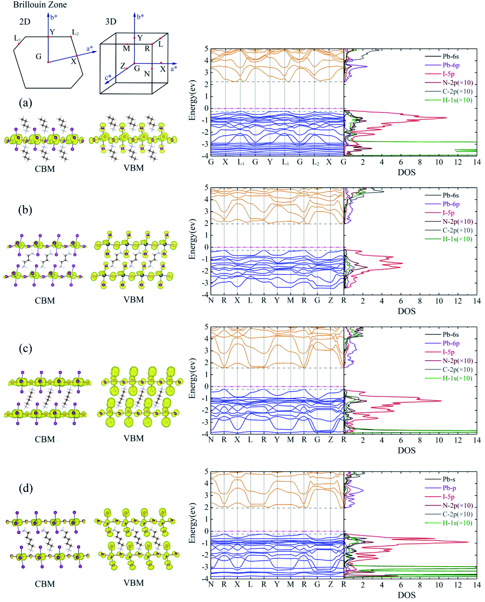 | ||
| Fig. 2 From left to right, densities at the VBM and CBM states (with an isosurface value of 0.0001 e Å−3), energy band structure, and density of states (DOS) for (a) BA2PbI4, (b) DPAPbI4, (c) BDAPbI4, and (d) PDAPbI4. “C-2p”, “N-2p”, and “H-1s” are increased ten times from the original value. Fermi level is marked with a magenta line. The inset in the upper left corner indicates the high-symmetry points in the first Brillouin zone of the 2D and 3D perovskites. | ||
We also calculated the band decomposed charge density of the CBM and the VBM (left side of Fig. 2 and S2†). All 2D and 3D perovskites showed similar results, indicating that the CBM state was mainly provided by the Pb atoms, and the VBM state was mainly derived from the I atoms. We also observe that the I atoms contributed slightly to the CBM states; however, only the I atoms in the Pb atomic layer contributed to it, and the I atoms between the two Pb atomic layers did not. It was shown that the effect of the six I atoms adjacent to the Pb atom on the formation of the energy band was not equivalent. In order to gain a deeper understanding of the electronic structures of these 2D and 3D perovskites, we analyzed the density of state (DOS) projected in the atomic orbital, as shown in the right side of Fig. 2 and S2.† The 6p orbital of the Pb atom constituted the VBM, and the 5p orbital of I constituted the CBM. In addition, the 5p orbital of I and the 6s orbital of Pb also contributed a little to the VBM and CBM, respectively. This is consistent with the above analysis of the band decomposed charge density of the CBM and VBM and the results of most theoretical calculations.35–37 These results indicated that the charge densities in the VBM and CBM states were distinctly separated in space. Evidently, a poor overlap of the charge density in the CBM and VBM states can lead to a low recombination transition rate in monoamino-2D and diamino-3D perovskites, which is conducive to low-loss photovoltaic devices. This result was consistent with the widely studied monoamino-3D perovskite materials (MAPbI3, FAPbI3, etc.). We can see that not only the I and Pb atoms but also the I and C, H, and N atoms undergo orbital hybridization due to the similar DOS in the wide energy range of 2–6 eV and −3–0 eV. Therefore, the interaction between the inorganic layer and the organic molecules was mainly undertaken by the I atoms, which is consistent with the calculation results of the differential charge density presented below.
The charge density difference (Fig. 3 and S3†) is used to reflect the charge transfer between the inorganic layer and the organic molecules and is given by the following formula:
| Δρ = ρperovskite − ρmolecule − ρPbI4 | (3) |
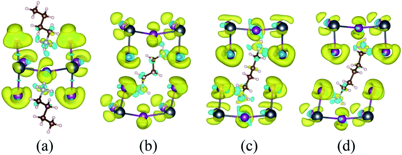 | ||
| Fig. 3 Charge density difference of (a) BA2PbI4, (b) DPAPbI4, (c) BDAPbI4, and (d) PDAPbI4 with an isosurface value of 0.0015 e Å−3. The yellow part indicates that electrons are obtained, and the blue part indicates electron loss. | ||
Similarly, ρPbI4 is the charge density of the inorganic PbI4 after removal of the organic molecules. The yellow and blue isosurfaces correspond to the electron increase and depletion zones, respectively. Evident charge transfers from monoamino and diamino group molecules to the I atoms were observed, as shown in Fig. 3 and S3.† The region where the electrons were obtained was mainly concentrated near the I atom, and the region where the monoamino and diamino groups were located lose electrons. This is also consistent with the results of our Bader charge analysis (Tables 2 and S1†). The number of electrons lost in the organic molecule of (BA)2PbI4, EDAPbI4, DPAPbI4, BDAPbI4, PDAPbI4, and HDAPbI4 was about 1.45e, 1.44e, 1.46e, 1.48e, 1.45e, and 1.47e, respectively. The (BA)2PbI4 contains two monoamino molecules (BA); however, there was only one diamino molecule in the other 3D perovskites (EDAPbI4, DPAPbI4, BDAPbI4, PDAPbI4, and HDAPbI4), so the number of charge losses for the diamino molecules were twice that of a single amino molecule. This shows that the monoamino molecule BA was a positive monovalent ion, while the diamino molecules (EDA, DPA, BDA, PDA, and HDA) were positive divalent ions. Therefore, it can be considered that all 2D and 3D materials were ionic, the ionicity of BDAPbI4 might be slightly stronger because the organic BDA ions lose an increased charge of about 1.48e.
| (BA)2PbI4 | DPAPbI4 | BDAPbI4 | PDAPbI4 | |||||||||
|---|---|---|---|---|---|---|---|---|---|---|---|---|
| Organic | −1.4473 | C | −1.2086 | −1.4585 | C | −1.0504 | −1.4836 | C | −0.9316 | −1.4521 | C | −1.0131 |
| H | −6.1407 | H | −6.3297 | H | −6.4050 | H | −6.3304 | |||||
| N | 5.9020 | N | 5.9216 | N | 5.8530 | N | 5.8913 | |||||
| Inorganic | 1.4473 | Pb | −1.1080 | 1.4585 | Pb | −1.0965 | 1.4836 | Pb | −1.1039 | 1.4521 | Pb | −1.1015 |
| I | 2.5553 | I | 2.5550 | I | 2.5875 | I | 2.5537 | |||||
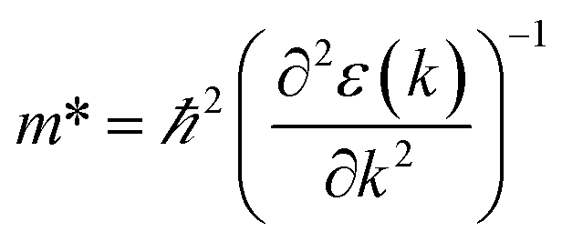
We calculated the effective mass of electrons in different directions (Table 3) according to the following equation:
 of BA2PbI4, EDAPbI4, DPAPbI4, BDAPbI4, PDAPbI4, and HDAPbI4. The values in the table are in m0, and “m0” is the static mass of a single electron
| KL1–X | KL1–Y | KL1–G | Average | ||
|---|---|---|---|---|---|
| BA2PbI4 |  |
0.856 | 0.971 | 0.362 | 0.729 |
 |
1.278 | 34.545 | 1.109 | 12.310 | |
| KR–M | KR–N | KR–L | KR–X | KR–Y | KR–Z | KR–G | Average | ||
|---|---|---|---|---|---|---|---|---|---|
| EDAPbI4 |  |
1.079 | 0.935 | 17.122 | 1.200 | 1.607 | 0.511 | 0.574 | 3.290 |
 |
1.436 | 13.995 | 0.513 | 1.456 | 2.067 | 1.305 | 0.956 | 3.104 | |
| DPAPbI4 |  |
1.119 | 0.863 | 2.932 | 1.306 | 1.725 | 0.483 | 0.461 | 1.270 |
 |
4.345 | 2.344 | 0.244 | 0.642 | 0.672 | 2.467 | 1.134 | 1.692 | |
| BDAPbI4 |  |
0.891 | 0.741 | 7.368 | 1.036 | 1.231 | 0.228 | 0.266 | 1.680 |
 |
0.909 | 0.480 | 0.465 | 0.842 | 0.610 | 0.660 | 0.535 | 0.643 | |
| PDAPbI4 |  |
0.887 | 0.672 | 8.097 | 0.909 | 1.119 | 0.245 | 0.290 | 1.746 |
 |
1.842 | 0.890 | 1.431 | 0.897 | 1.634 | 1.046 | 1.106 | 1.264 | |
| HDAPbI4 |  |
0.389 | 0.702 | 20.261 | 0.860 | 0.478 | 0.251 | 0.281 | 3.318 |
 |
0.860 | 0.653 | 63.785 | 0.701 | 1.058 | 0.568 | 0.630 | 9.751 | |
For 2D perovskite BA2PbI4, we calculated an effective mass of the KL1–X, KL1–Y, and KL1–Γ directions, as shown in the left side of Fig. 2. The average effective mass of the electrons of the 2D perovskite (BA)2PbI4 in the three K directions was 0.729m0, but the average effective mass of a hole was 12.310m0, which is very large. We noted that the effective mass of the electrons demonstrated no obvious anisotropy and was very small in all three K directions, no more than the static mass of electrons m0. In contrast, the effective mass of the hole showed significant anisotropy, and the effective mass in the direction of KL1–Y was very large, up to 34.545m0. From Fig. 1(a), we see that the I atom in the direction of base vector a was not equivalent to the I atom in the direction of base vector b. The I atom in the direction of b was obviously closer to the amino group of the BA molecule, which results in the obvious distortion of the position of the I atom. The I atom in the direction of vector a was mainly bound to the adjacent Pb atom and was less affected by the amino group. The band structure also confirmed that the VBM of BA2PbI4 was generally flatter and less dispersed between L1 and Y.
For the 3D perovskites, starting from point R, we selected the direction parallel to the three basic vectors (KR–M, KR–N and KR–L), the direction parallel to the facing line (KR–X, KR–Y and KR–Z), and the direction parallel to the body diagonal (KR–G). According to the calculation results of the average effective mass in the above seven high symmetric directions, it can be seen that the average effective mass values of DPAPbI4, BDAPbI4, and PDAPbI4 were relatively small and no more than 2m0. On the other hand, the effective mass of the electron and hole of EDAPbI4 and HDAPbI4 were much larger than 2m0. It can be seen that in all of the 3D perovskites, the effective mass of the electrons in the KR–M and KR–N directions was significantly smaller than in the KR–L direction, which was perpendicular to the Pb layer and along the base vector c. In addition, except for EDAPbI4, as the molecular chain grew longer, the effective mass of electrons in the KR–L direction increased significantly from 2.93m0 for DPAPbI4 to 20.26m0 for HDAPbI4. The reason EDAPbI4 did not satisfy this rule was that two I atoms in the adjacent Pb atomic layers were too close, and this resulted in mutual exclusion and a large distortion of the atomic arrangement (Fig. S1(a)†), thus increasing the effective mass in the KR–L direction. In this case, the so-called position distortion is that the direction of the connection of the two I atoms has a large angle relative to the c direction. Considering that the electrons at CBM are mainly supplied by the Pb atoms, with the increased length of the molecular chain, the interlayer spacing of the Pb atoms in the c direction increased from 10.20 Å for DPAPbI4 to 12.91 Å for HDAPbI4. Thus, the direct migration of electrons between the Pb atomic layers in this direction is bound to become more and more difficult. By comparing the effective mass of electrons in the different K directions, it was found that the effective mass of electrons in the body diagonal direction (KR–G) was the smallest. In addition, the effective masses in the face diagonal direction (KR–X and KR–Y) between the Pb atoms layers were between that in the body diagonal direction (KR–G) and that in the direction perpendicular to the Pb atoms layer (KR–L). These results indicated that the electron transport between the layers of the Pb atoms was easier to achieve by using organic molecules as bridges in the face diagonal and body diagonal directions.
It was found that, except for HDAPbI4, the effective mass of the holes was significantly smaller than the effective mass of the electrons in the KR–L direction. Considering that the holes at VBM were mainly provided by the I atoms, the distance between the I atoms in the two adjacent inorganic layers in the c direction was less than 5 Å (Table 1), and the valence wave functions of the I atoms overlap to some extent, which causes the hole carriers to migrate between the I atoms. At the same time, we also observed that with the increase in molecular chain length, the distance between the I atoms in the two adjacent inorganic layers in the c direction increased gradually, which led to the decrease of the overlap of the valence wave functions between the I atoms. As a result, the effective mass of the holes in the KR–L direction increased gradually, increasing to 63.785m0 in HDA PbI4, which had the largest distance between the I atoms at 6.42 Å. We found that in EDAPbI4 and DPAPbI4, the effective masses of the holes in the inorganic layers (KR–M and KR–N directions) were also larger, which may have been due to the larger position distortion of the atoms in the inorganic layers caused by diamino molecules with shorter chains, as shown in Fig. 1(b) and S1(a).† Comparing the effective masses of the electrons and holes in all K directions for the considered perovskites, we found that the effective masses of the electrons and holes for DPAPbI4, BDAPbI4, and PDAPbI4 were relatively close, although there were differences in the KR–L direction. However, the effective masses in most K directions were relatively small and similar to that observed for the monoamine-3D perovskites (MAPbI3, MASnI3, and FAPbI3).38,39 The carrier mobility is inversely proportional to the effective mass of the carrier. The effective masses of the electrons and holes in the three diamino-3D perovskites (DPAPbI4, BDAPbI4, and PDAPbI4) were light and balanced, which indicated that their transport properties were excellent. Generally, the interlayer transport properties of mono-amino 2D perovskite materials are poor. For example, 2D perovskite needs to be doped with TiO2 nanowire to improve the interlayer transport properties of the carriers.18
3.3 Optical absorption properties
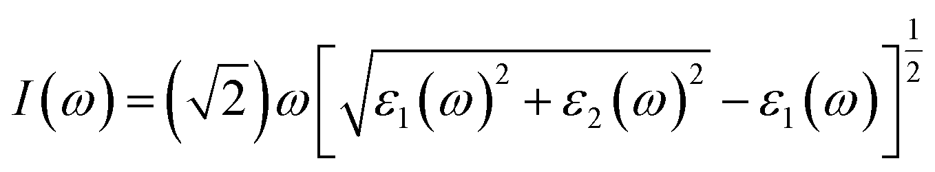
It is well known that an excellent candidate for solar energy conversion should have an appropriate bandgap, higher carrier mobility, low carrier recombination rate, as well as a high absorption coefficient. Thus, we simulated optical absorption spectra for all of the 2D and 3D perovskites, as shown in Fig. 4 and S4.† The absorption coefficient was calculated using the equation:5where ε1(ω) and ε2(ω) are the real and imaginary parts of the dielectric function, respectively, depending on the optical frequency ω.
 | ||
| Fig. 4 Absorption coefficients of (a) BA2PbI4, (b) DPAPbI4, (c) BDAPbI4, and (d) PDAPbI4. | ||
Significant anisotropic optical absorption occurs because of the existence of long-chain monoamino and diamino molecules present in the 2D and 3D perovskites. The range of light absorption energy along the direction of the maximum lattice constant c was blue-shifted compared with that in the Pb–I inorganic atomic layer, which corresponds to less light absorption in the wavelength range of 400–800 nm, but it contributes greatly to the absorption in the high energy range of less than 400 nm. It was also found that the larger the lattice constant c of the 3D perovskites (except EDAPbI4) corresponded to a more obvious blue shift of the optical absorption peak in the c direction. The apparent blue shift of the absorption energy range of EDAPbI4 in the c direction could also be attributed to the position distortion of the two adjacent I atoms between the inorganic layers, as the two I atoms would repel each other. In addition, larger optical absorption coefficients were observed in the wavelength range of 400–800 nm for all the considered 3D perovskites, which were larger than that of the 2D perovskite (BA2PbI4) in the same wavelength range. It is worth mentioning that the absorption edge of BDAPbI4 had the largest wavelength, which was consistent with the calculated bandgap. For the highest absorption coefficient up to 0.05–0.06 nm−1 for all the calculated 3D perovskites, even in the 550–600 nm wavelength range, the optical absorption coefficients reached 0.01 nm−1, which corresponding to 300 nm-thick perovskites that absorb 90% of the incident light. The 300 nm thickness is an optimized value present in several highly efficient planar heterojunction devices.40,41 Comparing all of the calculated perovskites, BDAPbI4 exhibit excellent optical absorption properties in the solar light irradiation range, and BDAPbI4 was predicted to exhibit the best photovoltaic performance among all calculated 2D and 3D perovskites, along with a light effective masses of the electrons and holes, a reduced bandgap, and a large optical absorption.
4. Conclusions
We studied the geometries, formation energies, electronic structures, and optical absorption properties of BA2PbI4, EDAPbI4, DPAPbI4, BDAPbI4, PDAPbI4, and HDAPbI4 via first-principles calculations. In general, the formation energy of the perovskite materials formed by diamino molecules with longer main chains was relatively low. Although the chain length of the diamino molecule in DPAPbI4 was the same as that of the monoamino molecule in BA2PbI4, the formation energy of DPAPbI4 was lower than that of BA2PbI4. We found that the bandgap and band structure depend on the symmetry of the crystal. Among the five 3D perovskite materials, the bandgap of BDAPbI4 was the narrowest direct bandgap at about 1.78 eV. All of the 2D and 3D perovskites showed similar results, in that the CBM state was mainly provided by the Pb atoms, and the VBM state was mainly derived from the I atoms in the Pb atomic layer. The charge densities in the VBM and CBM states were distinctly separated in space, and a poor overlap of the charge density in the CBM and VBM states could lead to a low recombination transition rate in the diamino-3D perovskites, which is beneficial for obtaining low-loss photovoltaic devices. The transport characteristics of the electrons in the different directions were analyzed by calculating the effective masses in the different directions. The effective masses of the electrons and holes in DPAPbI4, BDAPbI4, and PDAPbI4 were light and balanced, which indicated that their transport properties were excellent. In particular, BDAPbI4 exhibited excellent optical absorption properties in the solar light irradiation range, along with light effective masses of the electrons and holes, a reduced bandgap, and a large optical absorption. Together, these results will help the future design and synthesis of more efficient and stable organic–inorganic perovskite optoelectronic devices.Conflicts of interest
There are no conflicts to declare.Acknowledgements
The authors acknowledge the financial support from the National Natural Science Foundation of China (No. 61874008 and 61574014), Beijing Municipal Science and Technology Commission project (No. Z181100004718004), and National Training Program of Innovation and Entrepreneurship for Undergraduates (No. 201910004006).References
- A. Kojima, K. Teshima, Y. Shirai and T. Miyasaka, J. Am. Chem. Soc., 2009, 131, 6050–6051 CrossRef CAS PubMed.
- C. C. Stoumpos, C. D. Malliakas and M. G. Kanatzidis, Inorg. Chem., 2013, 52, 9019–9038 CrossRef CAS PubMed.
- National Renewable Energy Laboratory (NREL) Efficiency chart (2018), http//:www.nrel.gov/pv/assets/pdfs/pv-efficiency-chart.20181214.pdf.
- S. Ahmad, P. K. Kanaujia, H. J. Beeson, A. Abate, F. Deschler, D. Credgington, U. Steiner, G. V. Prakash and J. J. Baumberg, ACS Appl. Mater. Interfaces, 2015, 7, 25227–25236 CrossRef CAS PubMed.
- G. P. Nagabhushana, R. Shivaramaiah and A. Navrotsky, Proc. Natl. Acad. Sci. U. S. A., 2016, 113, 7717–7721 CrossRef CAS PubMed.
- T. A. Berhe, W. N. Su, C. H. Chen, C. J. Pan, J. H. Cheng, H. M. Chen, M. C. Tsai, L. Y. Chen, A. A. Dubale and B. J. Hwang, Energy Environ. Sci., 2016, 9, 323 RSC.
- C. W. Kim, T. Y. Eom, I. S. Yang, B. S. Kim, W. I. Lee, Y. S. Kang and Y. S. Kang, Sci. Rep., 2017, 7, 6849 CrossRef PubMed.
- G. Niu, W. Li, F. Meng, L. Wang, H. Dong and Y. Qiu, J. Mater. Chem. A, 2014, 2, 705 RSC.
- S. Shahbazi, M. Byranvand, F. Tajabadi, S. Afshar and N. Taghavinia, ChemPhysChem, 2016, 17, 2389–2394 CrossRef CAS PubMed.
- G. Niu, X. Guo and L. Wang, J. Mater. Chem. A, 2015, 3, 8970–8980 RSC.
- J. Schoonman, Chem. Phys. Lett., 2015, 619, 193–195 CrossRef CAS.
- I. C. Smith, E. T. Hoke, D. Solis-Ibarra, M. D. McGehee and H. I. Karunadasa, Angew. Chem., Int. Ed., 2014, 126, 11414–11417 CrossRef.
- D. H. Cao, C. C. Stoumpos, O. K. Farha, J. T. Hupp and M. G. Kanatzidis, J. Am. Chem. Soc., 2015, 137, 7843–7850 CrossRef CAS PubMed.
- H. Tsai, W. Nie, J. C. Blancon, C. C. Stoumpos, R. Asadpour, B. Harutyunyan, A. J. Neukirch, R. Verduzco, J. J. Crochet, S. Tretiak, L. Pedesseau, J. Even, M. A. Alam, G. Gupta, J. Lou, P. M. Ajayan, M. J. Bedzyk, M. G. Kanatzidis and A. D. Mohite, Nature, 2016, 536, 312–316 CrossRef CAS PubMed.
- L. N. Quan, M. Yuan, R. Comin, O. Voznyy, E. M. Beauregard, S. Hoogland, A. Buin, A. R. Kirmani, K. Zhao, A. Amassian, D. H. Kim and E. H. Sargent, J. Am. Chem. Soc., 2016, 138, 2649–2655 CrossRef CAS PubMed.
- S. Yang, Y. Wang, P. Liu, Y. B. Cheng, H. J. Zhao and H. G. Yang, Nat. Energy, 2016, 1, 15016 CrossRef CAS.
- C. C. Stoumpos, D. H. Cao, D. J. Clark, J. Young, J. M. Rondinelli, J. I. Jang, J. T. Hupp and M. G. Kanatzidis, Chem. Mater., 2016, 28, 2852–2867 CrossRef CAS.
- Y. Sanehira, Y. Numata, M. Ikegami and T. Miyasaka, Chem. Lett., 2017, 46, 1204–1206 CrossRef CAS.
- H. Tsai, W. Nie, J. C. Blancon, C. C. Stoumpos, R. Asadpour, B. Harutyunyan, A. J. Neukirch, R. Verduzco, J. J. Crochet, S. Tretiak, L. Pedesseau, J. Even, M. A. Alam, G. Gupta, J. Lou, P. M. Ajayan, M. J. Bedzyk, M. G. Kanatzidis and A. D. Mohite, Nature, 2016, 536, 312–316 CrossRef CAS PubMed.
- D. H. Cao, C. C. Stoumpos, O. K. Farha, J. T. Hupp and M. G. Kanatzidis, J. Am. Chem. Soc., 2015, 137, 7843–7850 CrossRef CAS PubMed.
- L. N. Quan, M. Yuan, R. Comin, O. Voznyy, E. M. Beauregard, S. Hoogland, A. Buin, A. R. Kirmani, K. Zhao, A. Amassian, D. H. Kim and E. H. Sargent, J. Am. Chem. Soc., 2016, 138, 2649–2655 CrossRef CAS PubMed.
- G. Kresse and J. Furthmüller, Comput. Mater. Sci., 1996, 6, 15–50 CrossRef CAS.
- P. E. Blöchl, Phys. Rev. B: Condens. Matter Mater. Phys., 1994, 50, 17953–17979 CrossRef.
- J. P. Perdew, K. Burke and M. Ernzerhof, Phys. Rev. Lett., 1996, 17, 3865–3868 CrossRef PubMed.
- S. Grimme, J. Antony, S. Ehrlich and S. Krieg, J. Chem. Phys., 2010, 132, 154104 CrossRef PubMed.
- W. Tang, E. Sanville and G. Henkelman, J. Phys.: Condens. Matter, 2009, 21, 084204 CrossRef CAS PubMed.
- E. Sanville, S. D. Kenny, R. Smith and G. Henkelma, J. Comput. Chem., 2007, 28, 899–908 CrossRef CAS PubMed.
- G. Henkelman, A. Arnaldsson and H. Jónsson, Comput. Mater. Sci., 2006, 36, 254–360 CrossRef.
- E. Mosconi, A. Amat, M. K. Nazeeruddin, M. Gratzel and F. De Angelis, J. Phys. Chem. C, 2013, 117, 13902–13913 CrossRef CAS.
- J. Even, L. Pedesseau, J.-M. Jancu and C. Katan, J. Phys. Chem. Lett., 2013, 4, 2999–3005 CrossRef CAS.
- B. Liu, M. Long and M. Cai, Nano Energy, 2019, 715–720 CrossRef CAS.
- M. M. Lee, J. Teuscher, T. Miyasaka, T. N. Murakami and H. J. Snaith, Science, 2012, 338, 643 CrossRef CAS PubMed.
- (a) D. A. Egger and L. Kronik, J. Phys. Chem. Lett., 2014, 5, 2728–2733 CrossRef CAS PubMed; (b) A. Amat, E. Mosconi, E. Ronca, C. Quarti, P. Umari, M. K. Nazeeruddin, M. Gratzel and F. D. Angelis, Nano Lett., 2014, 14, 3608–3616 CrossRef CAS PubMed.
- L. N. Quan, M. Yuan, R. Comin, O. Voznyy, E. M. Beauregard, S. Hoogland, A. Buin, A. R. Kirmani, K. Zhao, A. Amassian, D. H. Kim and E. H. Sargent, J. Am. Chem. Soc., 2016, 138, 2649–2655 CrossRef CAS PubMed.
- D. Li, C. Liang, H. Zhang, C. Zhang, F. You and Z. He, J. Appl. Phys., 2015, 117, 074901 CrossRef.
- D. Li, J. Meng, Y. Niu, H. Zhao and C. Liang, Chem. Phys. Lett., 2015, 627, 13–19 CrossRef CAS.
- D. Li, F. Sun, C. Liang and Z. He, J. Alloys Compd., 2018, 741, 489–494 CrossRef CAS.
- P. Umari, E. Mosconi and F. De Angelis, Sci. Rep., 2014, 4, 4467 CrossRef PubMed.
- A. Amat, E. Mosconi, E. Ronca, C. Quarti, P. Umari, M. K. Nazeeruddin, M. Gratzel and F. De Angelis, Nano Lett., 2014, 14, 3608–3616 CrossRef CAS PubMed.
- D. Liu and T. L. Kelly, Nat. Photonics, 2014, 8, 133 CrossRef CAS.
- Z. Xiao, C. Bi, Y. Shao, Q. Dong, Q. Wang, Y. Yuan, C. Wang, Y. Gao and J. Huang, Energy Environ. Sci., 2014, 7, 2619–2623 RSC.
Footnote |
| † Electronic supplementary information (ESI) available. See DOI: 10.1039/c9ra03042e |
| This journal is © The Royal Society of Chemistry 2019 |