DOI:
10.1039/C9RA03034D
(Paper)
RSC Adv., 2019,
9, 18157-18164
Sizable bandgaps of graphene in 3d transition metal intercalated defective graphene/WSe2 heterostructures†
Received
24th April 2019
, Accepted 29th May 2019
First published on 10th June 2019
Abstract
Controlling the electronic and magnetic properties of G/TMD (graphene on transition metal dichalcogenide) heterostructures is essential to develop electronic devices. Despite extensive studies in perfecting G/TMDs, most products have various defects due to the limitations of the fabrication techniques, and research investigating the performances of defective G/TMDs is scarce. Here, we conduct a comprehensive study of the effects of 3d transition metal (TM = Sc–Ni) atom-intercalated G/WSe2 heterostructures, as well as their defective configurations having single vacancies on graphene or WSe2 sublayers. Interestingly, Ni-intercalated G/WSe2 exhibits a small band gap of 0.06 eV, a typical characteristic of nonmagnetic semiconductors. With the presence of one single vacancy in graphene, nonmagnetic (or ferromagnetic) semiconductors with sizable band gaps, 0.10–0.51 eV, can be achieved by intercalating Ti, Cr, Fe and Ni atoms into the heterostructures. Moreover, V and Mn doped non-defective and Sc, V, Co doped defective G/WSe2 can lead to sizable half metallic band gaps of 0.1–0.58 eV. Further analysis indicates that the significant electron transfer from TM atoms to graphene accounts for the opening of a large band gap. Our results provide theoretical guidance to future applications of G/TMD based heterostructures in (spin) electronic devices.
1. Introduction
Heterogeneous systems like van der Waals heterostructures are of considerable interest due to their distinct physical and chemical properties,1–3 which opens an avenue for developing new types of applications for field-effect tunneling transistors,4–7 catalysis,8 solar cells,9 and so on. Among different heterogeneous systems, the heterogeneous bilayer structures constructed by locating the graphene (G) layer on proper two-dimensional substrates have been the focus of extensive research because of their potential in high-performance devices. In 2011, Chang and Chen found that G/MoS2 has excellent rate capability and cycling stability, and has the potential to act as an anode material for lithium ion batteries.10 In 2014, Tan et al. pointed out that the high electronic mobility of graphene could be maintained in the G/h-BN, G/GaSe and G/WS2 heterostructures.11 In 2015, Padilha et al.12 and Hu et al.13 found that the G/phosphorene (G/P) heterostructures can be utilized to control the Schottky barrier by applying a perpendicular electronic field. Using density functional theory calculations, Guo et al. found that the G/P heterostructures possess high capacity and good conductivity, excellent Li mobility and ultrahigh stiffness.14
Importantly, locating graphene on hetero-substrates could preserve a nearly linear band dispersion relation and open the band gap in graphene, which provides a strategy to overcome the biggest obstacle for its logical device application.15–21 As a few examples, theoretical studies have shown that the band gap of the G/h-BN heterostructure is sensitive to the interlayer spacing and stacking patterns.15,16 By applying a uniaxial electric field, the band structures of G/P heterostructures can be changed from semiconducting to metallic.17 In addition, a small band gap (2 meV) was opened for graphene when coupling it on MoS2 or MoSe2 substrate.18,19 Remarkably, sizable band gaps (3.9–28.2 meV) can be achieved for G/WS2 or G/MoS2 by regulating the stacking patterns and the interlayer spacing.20,21
Despite the progress, further improvement of the performances of the graphene-based heterostructures is still challenging. For example, although the weak interlayer van der Waals interaction can introduce small dispersion to the electronic structures of graphene, the opened band gap is too small to meet the requirement for nanodevice applications. With the aim of tuning the electronic and magnetic properties, intercalating atoms or molecules between bilayer 2D materials arises as an effective method.22–26 For example, by introducing Ti and Mn atoms between bilayer graphene, it is possible to transform them into semiconductors with sizable band gaps of 0.14 eV and 0.82 eV.23 In addition, due to the limitation of fabrication techniques, it is still challenging to synthesize large-area, high-quality 2D nanomaterials. Experimentally, a variety of defects: vacancies, interstitials, dopants and grain boundaries, and so on, will emerge unavoidably during the growth process of various 2D materials, which will greatly influence their performances.27–33 Unfortunately, few reports have been presented on the effects of such defects, and consequently, unveiling the influence of the defects on the performances of the heterostructures is of great importance. Different to MoS2, monolayer WSe2 is a p-type semiconductor and shows great potential for further electronic and spintronic applications. On the other hand, the fabrication of WSe2 appears to be somewhat more difficult, and therefore, the previously mentioned defects must appear in the samples.34–36 In this work, based on first-principles calculations, we have systematically studied the structural, electronic and magnetic properties of 3d transition metal atom (TM = Sc–Ni)-intercalated G/WSe2 heterostructures, as well as the systems involving single vacancies in graphene (G_sv) or WSe2 (WSe_svSe) sublayers. Based on the different features of the two-sublayers and the choice of the TM elements, the studied systems demonstrate different electronic and magnetic properties.
2. Models and method
All the calculations were performed within the framework of spin polarized DFT as implemented in the Vienna Ab initio Simulation Package (VASP).37,38 The exchange-correlation potentials were treated by the generalized gradient approximation (GGA) parameterized by Perdew, Burke and Ernzerhof (PBE).39 For the G/WSe2 heterostructures, the interaction between valence electrons and ion cores was described by the projector augmented wave (PAW) method40 and the DFT-D2 method41 was taken into account van der Waals (vdW) interaction. It is well accepted that the Coulomb interaction effect (Hubbard U) can help to describe well the magnetism of TM atoms. Comparing with the GGA calculations, the previously tested GGA + U (U = 3.1 eV) calculation in prior literature was proven to give nearly identical results regarding the magnetic features of these graphene/TMDCs systems.24,42–44 Therefore, we only explored the electronic and magnetic properties with the GGA method. The TM@(G/WSe2)s were modelled as a periodic slab by setting the lattice parameters as a = b = 9.88 Å (see Fig. 1a–c), in which a 4 × 4 supercell for the graphene and a 3 × 3 supercell for the WSe2 monolayer with the lattice mismatch of 1.1% were employed. The Monkhorst–Pack grid of 9 × 9 × 1 was used for the geometry optimization of G/WSe2 and a much more dense k point grid of 19 × 19 × 1 was set for electronic properties exploration. To ensure negligible interaction of the molecules from neighbouring unit cells, the lattice constant along the z axis was set as large as 16 Å. A 400 eV kinetic energy cutoff was chosen for the plane-wave basis set and conjugate gradient (CG) atomic optimization was performed with a criterion of convergence of 0.01 eV Å−1. For the test, we optimized the geometries of monolayer graphene and WSe2, and the lattice parameters were 2.47 Å and 3.33 Å (see Fig. 1a and b), respectively. On coupling the two sublayers, the interlayer distance of the G/WSe2 heterostructure is fully relaxed and optimized to be 3.37 Å and the band gap is made as small as approximately 1.0 meV. All the tested results are consistent with previous results,24,43 indicating that the computational methods we selected are reasonable.
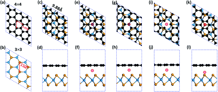 |
| | Fig. 1 Schematic illustrations of (a) monolayer graphene, (b) monolayer WSe2, (c and d) G/WSe2, (e and f) TM@(G/WSe2), (g and h) TM@(G_sv/WSe2), (i and j) TM@(G_sv2/WSe2), (k and l) TM@(G/WSe_svSe) heterostructures. Black, yellow, cyan and red balls represent C, Se, W and 3d TM atoms, respectively. | |
3. Results and discussion
Four types of TM intercalated G/WSe2 configurations were considered: (i) TM@(G/WSe2)s, in which the TM atoms are located between the hollow site of graphene and the top site of a W atom in the WSe2 layer (see Fig. 1e and f); (ii) and (iii) TM@(G_sv/WSe2)s and TM@(G_sv2/WSe2)s, wherein the graphene layer has a single vacancy and the TM atom is just located between the vacancy of graphene and the top site of a W atom (ii) (see Fig. 1g and h) or the hollow site of the WSe2 layer (iii) (see Fig. 1i and j); (iv) TM@(G/WSe_svSe)s, where the WSe2 sublayer has a single Se vacancy and the TM atom is put directly between the vacancy and the hollow site of graphene (see Fig. 1k and l). All the optimized structures are presented in Fig. S1–S4 in the ESI,† and most systems intercalated with TM atoms almost maintain their initial configurations. Exceptions are found for the Co and Ni intercalated G/WSe2, where the graphene layer slides slightly with respect to the WSe2 sublayer and the TM atoms sit away from the hollow site of graphene. In TM@(G/WSe2)s, the distances from TM atoms to the graphene layer are around 1.74–2.25 Å, which are much larger than those between TMs and WSe2 layers, ∼1.11–1.68 Å (see Fig. S5 in the ESI†). In addition, introducing one single vacancy to graphene largely shortens the TM–G distances, ∼0.94–1.22 Å, while in the case of TM@(G/WSe_svSe)s, the TM atoms almost fill the Se vacancy.
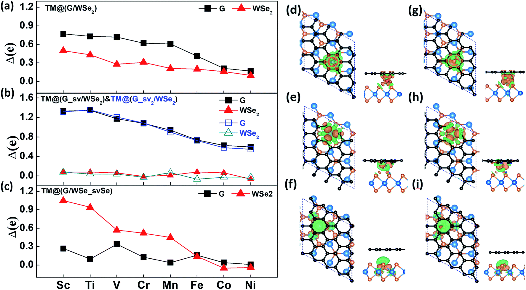
In general, the charge transfer to graphene and WSe2 layers decreases gradually from Sc- to Ni-doped systems according to the Bader charge analysis (see Fig. 2a–c). In the case of defective systems, charge transfer to the defective graphene or WSe2 layers is largely enhanced, which is caused by the shortened distances of TM atoms to the graphene or WSe2 layer with one single vacancy (see Fig. S5 in the ESI†). Fig. 2d–i depict the charge density differences (CDDs) of six Mn/Fe intercalated G/WSe2 systems, defined as Δρ = ρ[sys] − ρ[TM] − ρ[G] − ρ[WSe2], where ρ[●] is the charge density of the whole system, the TM atom, graphene, and WSe2, respectively. The charges are transferred from TM atoms to the graphene and WSe2 sublayers, and the TM–G (TM–WSe2) interaction displays obvious covalent bonding character. The binding energies of these systems are calculated by the equation, Eb = ETM + EG + EWSe2 − Esys, where the ETM, EG, EWSe2 and Esys represent the total energy of the TM atoms, graphene, WSe2, and the whole system, respectively. All the structures were found to be thermodynamically stable for having large binding energies (3.52–11.73 eV) (see Table 1), much larger than those of TM adsorbed graphene.45 Of these, the binding energies of the systems with a defective graphene or WSe2 layer (∼5.16–11.73 eV) are much larger than those of TM@(G/WSe2)s (∼3.52–5.89 eV) and other TM@(G/TMD)s.24
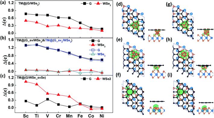 |
| | Fig. 2 (a–c) The charges transferred to the graphene layer and the WSe2 layer in TM@(G/WSe2)s, TM@(G_sv/WSe2)s, TM@(G_sv2/WSe2)s and TM@(G/WSe_svSe)s, respectively. (d–i) Top and side views of the CDDs plots for TM@(G/WSe2)s, TM@(G_sv/WSe2)s and TM@(G/WSe_svSe)s (TM = Mn, Fe), respectively. Orange and green isosurfaces denote the accumulation and depletion of electrons, respectively. The isosurface value is ±0.03 e Å−3. | |
Table 1 The binding energies (Eb), magnetic moments (MMs) and ground states (GS) of TM@(G/WSe2)s, TM@(G_sv/WSe2)s, TM@(G_sv2/WSe2)s and TM@(G/WSe_svSe)s intercalated with different TM atoms. Here “FM” stands for ferromagnetic state, “NM” for nonmagnetic state, “AFM” for antiferromagnetic state, “M” for metal, “SC” for semiconductor and “HM” for half metal
| Sys |
TM@(G/WSe2) |
TM@(G_sv/WSe2) |
TM@(G_sv2/WSe2) |
TM@(G/WSe_svSe) |
| Eb (eV) |
MM (μB) |
GS |
Eb (eV) |
MM (μB) |
GS |
Eb (eV) |
MM (μB) |
GS |
Eb (eV) |
MM (μB) |
GS |
| Sc |
5.55 |
1.80 |
FM M |
9.30 |
0.72 |
FM HM |
9.16 |
0.27 |
FM M |
7.54 |
0 |
AFM M |
| Ti |
5.89 |
2.46 |
FM M |
10.87 |
0 |
NM SC |
10.71 |
0 |
NM SC |
7.64 |
0 |
NM M |
| V |
5.37 |
3.81 |
FM HM |
10.68 |
1.00 |
FM HM |
10.38 |
1.00 |
FM HM |
6.31 |
0 |
AFM M |
| Cr |
3.52 |
4.30 |
FM M |
9.46 |
2.00 |
FM SC |
9.2 |
2.00 |
FM SC |
5.16 |
0 |
AFM M |
| Mn |
3.61 |
3.05 |
FM HM |
9.29 |
3.00 |
FM M |
9.24 |
3.00 |
FM M |
5.76 |
3.05 |
FM M |
| Fe |
5.85 |
2.02 |
FM HM |
11.73 |
0 |
NM SC |
11.530 |
0 |
NM SC |
7.37 |
0 |
AFM M |
| Co |
5.23 |
1.00 |
FM HM |
10.68 |
0.96 |
FM HM |
10.64 |
0.88 |
FM HM |
6.35 |
1.05 |
FM M |
| Ni |
5.80 |
0 |
NM SC |
9.79 |
0 |
NM SC |
9.77 |
0 |
NM SC |
6.88 |
0 |
NM M |
Interestingly, versatile electronic and magnetic behaviors are identified for these TM intercalated G/WSe2 structures (see Table 1). To accurately explore the real magnetic ground states of such TM@(G/WSe2)s, we adopted the 2 × 1 × 1 supercell including two TM atoms to compare the stabilities of their FM and AFM coupling. The TM@(G/WSe2)s at TM = Sc–Co demonstrate robust ferromagnetism (FM) with magnetic moments of 1.80 μB, 2.46 μB, 3.81 μB, 4.30 μB, 3.05 μB, 2.02 μB and 1.00 μB per unit cell, respectively. In contrast, Ni@(G/WSe2) has a nonmagnetic (NM) ground state. Such magnetic moments are similar to those of TM adsorbed graphene45,46 or other TM@(G/TMDC)s.24 The magnetic properties of these TM-intercalated G/WSe2 heterostructures can be well understood from the partial density of states (PDOS) (see Fig. 3, S6 and S7 in the ESI†). In the crystal field of graphene and WSe2, the five d orbitals of TM atoms are split into two degenerate (dxy, dx2−y2) and (dxz, dyz) orbitals and one singly occupied dz2 orbital. Clearly, the TM–G or TM–WSe2 interaction upshifts the Fermi level of graphene or WSe2 simultaneously, and the impurity states are formed near the Fermi level. The magnetic moments of these systems are mainly contributed to by the 3d electrons of TM atoms, meaning fewer come from their nearby atoms in the graphene and WSe2 layers. Moreover, tunable electronic properties are identified for these TM intercalated G/WSe2 heterostructures. Similar to those TM@(G/MoS2)s,24 the TM@(G/WSe2) at TM = Sc, Ti and Cr are found to be metals, while those with TM = V, Mn, Fe, and Co are half metals (HM) (electrons of one spin orientation act as metals, while those of the opposite orientation act as semiconductors or insulators) having HM gaps of 0.10 eV, 0.13 eV, 0.05 eV and 0.06 eV, respectively (see Fig. 3 and S8a–g in the ESI†). In contrast, Ni@(G/WSe2) is a perfect semiconductor (SC) with a direct band gap of 0.06 eV (see Fig. S8h in the ESI†), which is much larger than those in pristine G/TMDs heterostructures.10,29,30
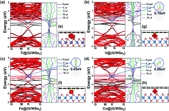 |
| | Fig. 3 (a–d) Plots of band structures and partial density of states (PDOS) and (e–h) spin densities of TM@(G/WSe2)s, TM = Ti, V, Fe, and Co, respectively. Red and black lines represent the bands of spin up and spin down, respectively. | |
Furthermore, introducing one single vacancy in graphene changes the stability, electronic and magnetic properties of TM@(G/WSe2)s significantly (see Table 1, Fig. 4, S9 and S10 in the ESI†). Compared with pristine TM@(G/WSe2)s, the binding energies of these graphene-defective systems become much larger, approximately 9.16–11.73 eV, and somewhat larger than those of the TM adsorbed single-vacancy graphene.45 Moreover, an FM to NM transition occurs from TM@(G/WSe2)s (TM = Ti, Fe) to their defective configurations of TM@(G_sv/WSe2)s or TM@(G_sv2/WSe2)s (see Fig. 4a, c, e and g). Apart from this, the TM@(G_sv/WSe2)s and TM@(G_sv2/WSe2)s (TM = Sc, V, Cr, Mn, Co) systems are FM. Their total magnetic moments are 0.72 μB, 1.00 μB, 2.00 μB, 3.00 μB, 0.96 μB and 0.27 μB, 1.00 μB, 2.00 μB, 3.00 μB, 0.88 μB per unit cell, respectively (see Table 1). In addition, a metal to SC transition occurs for TM@(G_sv/WSe2)s and TM@(G_sv2/WSe2)s at TM = Ti, Cr (see Fig. 4a, b, e and f), while a HM to SC transition is found for those doped with Fe atoms (see Fig. 4c and g). Apart from this, the TM@(G_sv/WSe2)s and TM@(G_sv2/WSe2)s at TM = V, Co and Ni retain the same electronic properties (see Fig. 4d, h, S9c, g, h, S10c, g and h in the ESI†). The HM gaps for TM@(G_sv/WSe2)s or TM@(G_sv2/WSe2)s (TM = V, Co) are 0.36 eV/0.58 eV and 0.29 eV/0.52 eV, respectively. The semiconducting properties of TM@(G_sv/WSe2)s or TM@(G_sv2/WSe2)s at TM = Ti, Cr and Fe atoms are similar to their G_svTMG isomers.46 Excepting Ni@(G_sv2/WSe2), which is a direct band gap SC, all the other SCs have indirect band gaps. It should be mentioned that all the SCs have much larger band gaps (0.10–0.51 eV) than those of G/TMDs and non-defective TM@(G/WSe2)s.18–21,42 A metal to HM transition occurs for Sc@(G_sv/WSe2), while the metallic state is maintained for Sc@(G_sv2/WSe2) (see Fig. S9a and S10a in the ESI†). For both Mn@(G_sv/WSe2) and Mn@(G_sv2/WSe2), a HM to metal transition is observed (see Fig. S9e and Fig. S10e in the ESI†).
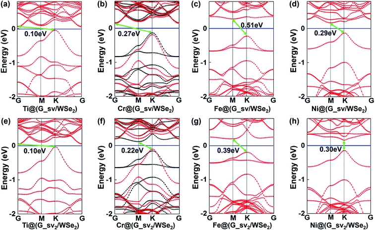 |
| | Fig. 4 Band structures of TM@(G_sv/WSe2)s (a–d) and TM@(G_sv2/WSe2)s (e–h), TM = Ti, Cr, Fe, Ni, respectively. Red and black lines represent the bands of spin up and spin down, respectively. | |
The tunable electronic properties of TM@(G/WSe2), TM@(G_sv/WSe2) and TM@(G_sv2/WSe2) can be well understood from the electronic configurations near the Fermi level. As shown in Fig. 2b and c, introducing a single vacancy in graphene redistributes the valence electrons of the systems. The impurity states around the Fermi level are mainly from the hybridized d(TM)–π(G) states (Fig. S6 and S7†). For TM@(G_sv/WSe2) and TM@(G_sv2/WSe2) with TM = Ti, Fe, two hybridized peaks on the majority/minority manifolds of their pristine configurations disappear, meaning that approximately two d electrons from the TM atom are transferred to the C vacant site (see Fig. S6a–c and S7a–c in the ESI†). In addition, the electrons on two spin manifolds distribute evenly, and these systems are thus changed to become NM (see Fig. S6b, c, S7b and c in the ESI†). For the V and Co doped TM@(G_sv/WSe2) or TM@(G_sv2/WSe2), approximately two flat bands from the minority folds disappear and become empty, leaving the majority bands to stay around the downshifted Fermi level. As a result, they are changed to FM HMs (see Fig. S6e, f, S7e and f in the ESI†). Similar to TM@(G_sv/WSe2)s or TM@(G_sv2/WSe2)s, the Ti- and Ni-intercalated (G/WSe_svSe)s are NM and those that are Mn- and Co-intercalated have FM ground states (see Table 1). In contrast, the introduction of an Se vacancy transforms four TM@(G/WSe_svSe)s (TM = Sc, V, Cr, Fe) to AFM (see Table 1). Furthermore, all the studied TM@(G/WSe_svSe)s are found to be metals (see Fig. S11 in the ESI†), wherein the Dirac cones of graphene in most systems are preserved in the Se vacant systems. Particularly, semimetal is identified for Ni@(G/WSe_svSe) (see Fig. S11h in the ESI†).
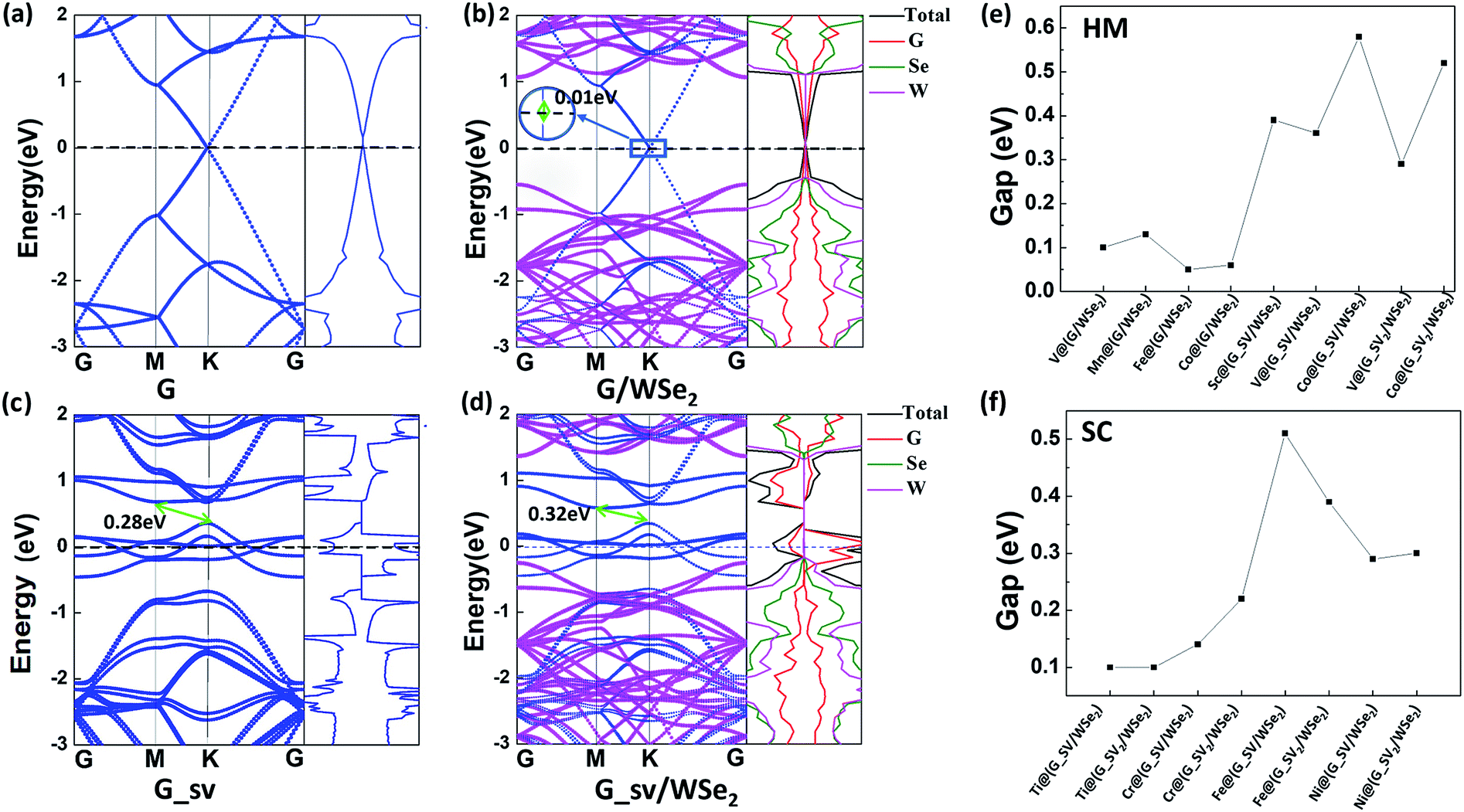
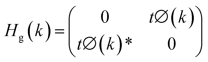
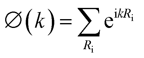
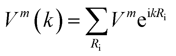
Finally, let's come to the wide band gaps of half metallic or semiconducting TM@(G_sv/WSe2)s and TM@(G_sv2/WSe2)s. The band structures of free-standing graphene, G/WSe2 and their defective counterparts are plotted in Fig. 5a–d. Clearly, a very small band gap (∼1 meV) is opened for graphene by adding the WSe2 substrate (see Fig. 5b). Remarkably, making a single vacancy on graphene is an effective way to introduce a sizable band gap. For free standing graphene with a single vacancy, a band gap of 0.28 eV (see Fig. 5c) can be easily obtained. The band gap can be further enlarged to 0.32 eV by adding the WSe2 substrate (see Fig. 5d). However, the Fermi level of both systems is downshifted, rendering a metal system. Interestingly, if more TM atoms are intercalated, SC or HM with a sizable band gap (both spin or one spin) can be formed (see Fig. 5e and f). Such large gaps for graphene-defective TM@(G_sv/WSe2)s and TM@(G_sv2/WSe2)s systems can be simply understood in terms of the quasi-particle scattering theory.24 As discussed above, there is obvious charge transfer between TM atoms and the graphene or WSe2 layer (see Fig. 2a–c). The local density of states of graphene in momentum space representation is given by the imaginary part of the Green's function:
| |
 | (1) |
 |
| | Fig. 5 (a–d) Plots of band structures and DOS of pristine graphene (a), G/WSe2 (b), graphene with a single vacancy (c) and G_sv/WSe2 (d). (e and f) Band gaps of HM and SC systems. | |
The Green's function of graphene in the presence of a single impurity
| |
 | (2) |
where
| |
 | (3) |
| |
 | (4) |
with
| |
 | (5) |
In graphene,
| |
 | (6) |
where

,

.
Using the local density of states of graphene, we find that the gaps of graphene are moderately opened by the impurity atoms. As shown in Fig. 1, our systems are studied based on the 4 × 4 supercell lattice, and accordingly, the scattering potential of the impurity atom in the lattice can be viewed as a periodic potential. As a result, the gap in the local density of states is a natural result. The new result of our findings is that the opened gap depends on the electron transfer between the impurity and graphene. For Ni@(G/WSe2), with small electron transfer between the Ni atom and graphene, the band gap is relatively small. However, in the case of TM@(G_sv/WSe2)s and TM@(G_sv2/WSe2)s systems (TM = Ti, Cr, Fe, Ni), significant electron transfer between the TM atom and graphene is obtained, accounting for large band gap opening (see Fig. 2).
4. Conclusions
Using the density functional theory method, we have systematically studied the structural, electronic and magnetic properties of 3d transition metal atom-intercalated pristine and defective G/WSe2 heterostructures. Obvious covalent bonding characters are identified for the TM–graphene and TM–WSe2 interactions. Different from perfect TM@(G/WSe2)s, introducing a single vacancy in the graphene layer or the WSe2 layer stabilizes the chemical bonding between the TM atoms and graphene layers. Interestingly, versatile electronic and magnetic properties are found. For the G/WSe2s having defective graphene layers, the systems doped with Ti, Fe and Ni atoms can lead to nonmagnetic semiconductors, while those with Cr atoms result in ferromagnetic semiconductors. All these proposed configurations show sizable band gaps ranging from 0.1 eV to 0.51 eV. In addition, V and Mn doped non-defective G/WSe2 and Sc, V, Co doped defective G/WSe2 can lead to sizable half metallic band gaps ranging from 0.1 eV to 0.58 eV. Our findings propose an effective way to manipulate the electronic and magnetic properties of graphene/TMD heterostructures.
Conflicts of interest
There are no conflicts of interest to declare.
Acknowledgements
This work is supported by the NSFC (11574262), the Qinglan Project of Jiangsu Province, the Personnel Training Plan of Yangzhou University, and the Scientific Research Foundation of Hebei Normal University (L2018B03).
References
- J. M. Hamm and O. Hess, Science, 2013, 340, 1298–1299 CrossRef PubMed.
- A. K. Geim and I. V. Grigorieva, Nature, 2013, 499, 419 CrossRef CAS PubMed.
- G. Gao, W. Gao, E. Cannuccia, J. Taha-Tijerina, L. Balicas and A. Mathkar, Nano Lett., 2012, 12, 3518 CrossRef CAS PubMed.
- L. Britnell, R. V. Gorbachev, R. Jalil, B. D. Belle, F. Schedin, A. Mishchenko and T. Georgiou, Science, 2012, 335, 947 CrossRef CAS PubMed.
- C. J. Shih, Q. H. Wang, Y. Son, Z. Jin, D. Blankschtein and M. S. Strano, ACS Nano, 2014, 8, 5790 CrossRef CAS PubMed.
- M. S. Choi, G. H. Lee, Y. J. Yu, D. Y Lee, S. H. Lee, P. Kim, W. J. Hone and J. Yoo, Nat. Commun., 2013, 4, 1624 CrossRef PubMed.
- H. Wang, L. Yu, Y. H. Lee, Y. Shi, A. Hsu, M. L. Chin, L. J. Li, M. Dubey, J. Kong and T. Palacios, Nano Lett., 2012, 12, 4674 CrossRef CAS PubMed.
- Y. X. Deng, Z. Luo, N. J. Conrad, H. Liu, Y. J. Gong, S. Najmaei, P. M. Ajayan, J. Lou, X. F. Xu and P. D. Ye, ACS Nano, 2014, 8, 8292 CrossRef CAS PubMed.
- H. J. J. Ling, C. Zhang, Y. P. Feng and L. Shen, Appl. Phys. Lett., 2016, 108, 122105 CrossRef.
- K. Chang and W. X. Chen, Chem. Commun., 2011, 47, 4252 RSC.
- J. Y. Tan, A. Avsar, J. Balakrishnan, G. K. W. Koon and T. Taychatanapat, Appl. Phys. Lett., 2014, 104, 183504 CrossRef.
- J. E. Padilha, A. Fazzio and J. R. Antônio da Silva, Phys. Rev. Lett., 2015, 114, 066803 CrossRef CAS PubMed.
- W. Hu, T. Wang and J. L. Yang, J. Mater. Chem. C, 2015, 3, 4756 RSC.
- G. C. Guo, D. Wang, X. L. Wei, Q. Zhang, H. Liu, W. M. Lau and L. M. Liu, J. Phys. Chem. Lett., 2015, 6, 5002 CrossRef CAS PubMed.
- G. Giovannetti, P. A. Khomyakov, G. Brocks, P. J. Kelly and J. van den Brink, Phys. Rev. B: Condens. Matter Mater. Phys., 2007, 76, 073103 CrossRef.
- Y. C. Fan, M. W. Zhao, Z. H. Wang, X. J. Zhang and H. Y. Zhang, Appl. Phys. Lett., 2011, 98, 083103 CrossRef.
- A. Hashmi, U. Farooq and J. Hong, Curr. Appl. Phys., 2016, 16, 318 CrossRef.
- Y. D. Ma, Y. Dai, W. Wei, C. W. Niu, L. Yu and B. B. Huang, J. Phys. Chem. C, 2011, 115, 20237 CrossRef CAS.
- C. J. Jin, F. A. Rasmussen and K. S. Thygesen, J. Phys. Chem. C, 2015, 119, 19928 CrossRef CAS.
- S. S. Li and C. W. Zhang, J. Appl. Phys., 2013, 114, 183709 CrossRef.
- Z. L. Wang, Q. Chen and J. L. Wang, J. Phys. Chem. C, 2015, 119, 4752 CrossRef CAS.
- H. K. Jeon, M. Maruyama, K. J. Kawahara, Y. Terao, D. Ding, R. Matsumoto, Y. Matsuo, S. Okada and H. Ago, Adv. Mater., 2017, 29, 1702141 CrossRef PubMed.
- X. Y. Zhang, X. L. Zhao and Y. J. Liu, J. Phys. Chem. C, 2016, 120, 22710 CrossRef CAS.
- X. Y. Zhang, Z. J. Bao, X. S. Ye, W. X. Xu and Y. J. Liu, Nanoscale, 2017, 9, 11231 RSC.
- M. Rafique, Y. Shuai, I. Ahmed, R. Shaikh, M. AliTunio and H. P. Tan, RSC Adv., 2018, 8, 23688 RSC.
- X. S. Zhou, L. J. Wan and Y. G. Guo, Chem. Commun., 2013, 4, 1838 RSC.
- X. Y. Zhang, Z. W. Xv, Q. H. Yuan, X. John and F. Ding, Nanoscale, 2015, 7, 20082 RSC.
- Y. Shi, W. Zhou, A. Y. Lu, W. Fang, Y. H. Lee, A. L. Hsu, S. M. Kim, K. K. Kim, H. Y. Yang, L. J. Li, J. C. Idrobo and J. Kong, Nano Lett., 2012, 12, 2784 CrossRef CAS PubMed.
- L. L. Yu, Y. H. Lee, X. Ling, J. G. Santos Elton, Y. C. Shin, Y. X. Lin, M. Dubey, E. Kaxiras, J. Kong, H. Wang and T. Palacios, Nano Lett., 2014, 14, 3055 CrossRef CAS PubMed.
- T. Georgiou, R. Jalil, B. D. Belle, L. Britnell, R. V. Gorbachev, S. V. Morozov, Y. J. Kim, A. Gholinia, S. J. Haigh and O. Makarovsky, Nat. Nanotechnol., 2013, 8, 100 CrossRef CAS PubMed.
- Y. C. Lin, N. Lu, L. J. Nestor Perea-Lopez, Z. Lin, X. Peng, C. H. Lee, C. Sun, L. Calderin, P. N. Browning, M. S. Bresnehan, M. J. Kim, T. S. Mayer, M. Terrones and J. A. Robinson, ACS Nano, 2014, 8, 3715 CrossRef CAS PubMed.
- F. Banhart, J. Kotakoski and A. V. Krasheninnikov, ACS Nano, 2011, 5, 26 CrossRef CAS PubMed.
- O. V. Yazyev and L. Helm, Phys. Rev. B: Condens. Matter Mater. Phys., 2007, 75, 125408 CrossRef.
- B. Liu, M. Fathi, L. Chen, A. Abbas, Y. Ma and C. Zhou, ACS Nano, 2015, 9, 6119 CrossRef CAS PubMed.
- J. Y. Chen, B. Liu, Y. P. Liu, W. Tang, C. T. Nai, L. J. Li, J. Zheng, L. B. Gao, Y. Zheng, H. S. Shin, H. Y. Jeong and K. P. Loh, Adv. Mater., 2015, 27, 6722 CrossRef CAS PubMed.
- Q. L. Feng, M. J. Zhu, Y. h. Zhao, H. Y. Liu, M. Li, J. B. Zheng, H. Xu and Y. M. Jiang, Nanotechnology, 2019, 30, 034001 CrossRef CAS PubMed.
- G. Kresse and J. Hafner, Phys. Rev. B: Condens. Matter Mater. Phys., 1993, 48, 13115 CrossRef CAS.
- G. Kresse and J. Furthmüller, Comput. Mater. Sci., 1996, 6, 15 CrossRef CAS.
- J. P. Perdew, K. Burke and M. Ernzerhof, Phys. Rev. Lett., 1996, 77, 3865 CrossRef CAS PubMed.
- P. E. Blochl, Phys. Rev. B: Condens. Matter Mater. Phys., 1994, 50, 17953 CrossRef.
- S. J. Grimme, Comput. Chem., 2006, 27, 1787 CrossRef CAS PubMed.
- T. O. Wehling, A. I. Lichtenstein and M. I. Katsnelson, Phys. Rev. B: Condens. Matter Mater. Phys., 2011, 84, 235110 CrossRef.
- S. Li, Z. M. Ao, J. J. Zhu, J. C. Ren, J. Yi, G. Wang and W. Liu, J. Phys. Chem. Lett., 2017, 8, 1484 CrossRef CAS PubMed.
- G. L. Zhang, R. L. Zhou, Y. Gao and X. C. Zeng, J. Phys. Chem. Lett., 2012, 3, 151–156 CrossRef CAS.
- X. J. Liu, C. Z. Wang, Y. X. Yao, W. C. Lu, M. Hupalo, A. C. Tringides and K. M. Ho, Phys. Rev. B: Condens. Matter Mater. Phys., 2011, 83, 235411 CrossRef.
- H. Johll and H. C. Kang, Phys. Rev. B: Condens. Matter Mater. Phys., 2009, 79, 245416 CrossRef.
Footnote |
| † Electronic supplementary information (ESI) available. See DOI: 10.1039/c9ra03034d |
|
| This journal is © The Royal Society of Chemistry 2019 |
Click here to see how this site uses Cookies. View our privacy policy here. 
 Open Access Article
 This Open Access Article is licensed under a Creative Commons Attribution-Non Commercial 3.0 Unported Licence
 *a,
Yi Suna,
Weicheng Gaoa,
Yin Lina,
Xinli Zhaoa,
Qiang Wanga,
Xiaojing Yao
*a,
Yi Suna,
Weicheng Gaoa,
Yin Lina,
Xinli Zhaoa,
Qiang Wanga,
Xiaojing Yao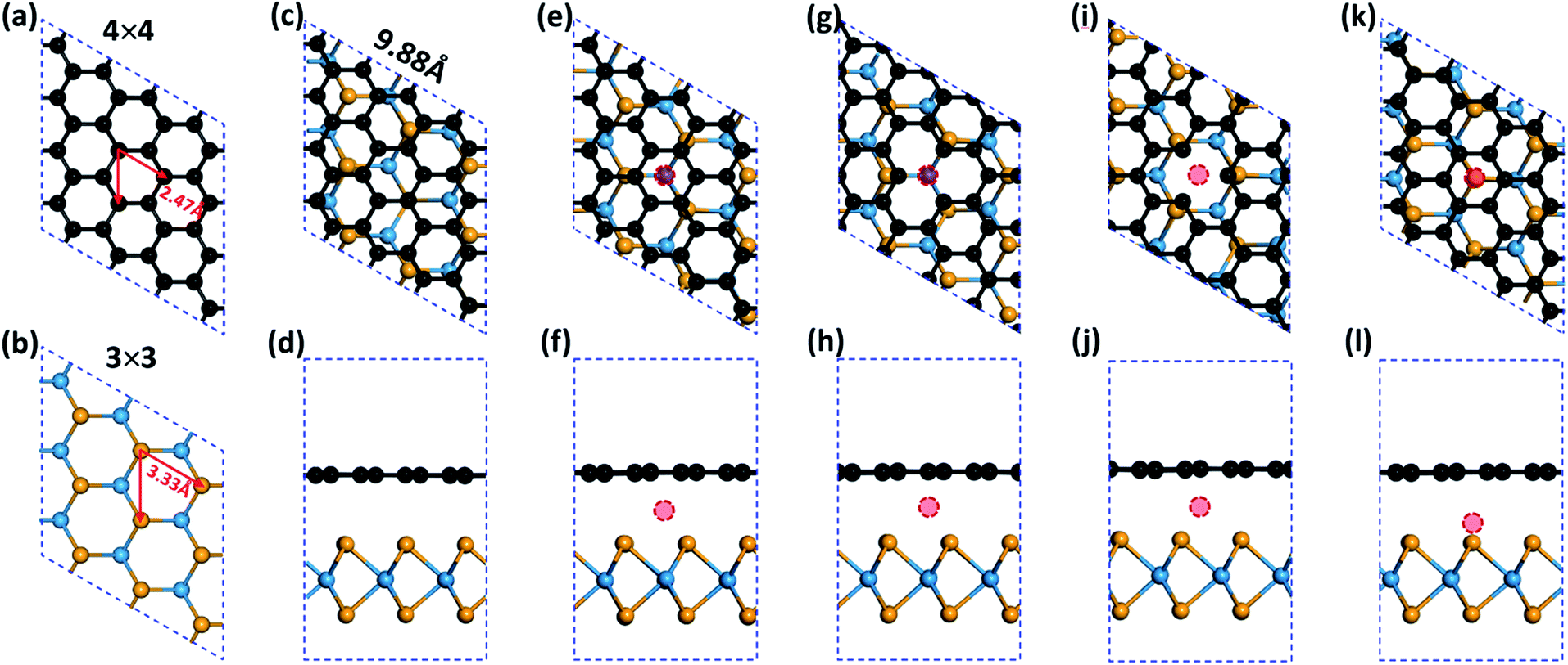


 ,
,  .
.