DOI:
10.1039/C9RA03006A
(Paper)
RSC Adv., 2019,
9, 22302-22312
The role of cobalt doping in tuning the band gap, surface morphology and third-order optical nonlinearities of ZnO nanostructures for NLO device applications
Received
23rd April 2019
, Accepted 14th June 2019
First published on 18th July 2019
Abstract
The work presented here reported the effect of doping cobalt (Co) in ZnO thin films. The thin films were prepared using the spray pyrolysis technique with 0, 1, 5 and 10 wt% cobalt doping concentrations to study the morphological, optical and third-order nonlinear optical (NLO) properties. X-ray diffraction revealed the crystalline nature of the prepared thin films, and the crystallite size was found to increase with the concentration of doped Co. The morphology and surface topography of the films were largely influenced by doping, as indicated by field emission scanning electron microscopy (FESEM) and atomic force microscopy (AFM). With an increase in Co-doping concentration, the direct optical energy band-gap value increased from 3.21 eV to 3.45 eV for pure to 10 at% of Co concentrations respectively. To study the NLO properties of the prepared thin films, the Z-scan technique was adopted; it was observed that with an increase in the doping concentration from 0 to 10 wt%, the nonlinear absorption coefficient (β) was enhanced from 4.68 × 10⁻³ to 9.92 × 10⁻³ (cm W−1), the nonlinear refractive index (n2) increased from 1.37 × 10⁻⁸ to 2.90 × 10⁻⁸ (cm2 W−1), and the third-order NLO susceptibility (χ(3)) values also increased from 0.79 × 10⁻⁶ to 1.88 × 10⁻⁶ (esu). At the experimental wavelength, the optical limiting (OL) features of the prepared films were explored, and the limiting thresholds were calculated. The encouraging results of the NLO studies suggest that the Co![[thin space (1/6-em)]](https://www.rsc.org/images/entities/char_2009.gif) :ZnO thin film is a capable and promising material for nonlinear optical devices and optical power limiting applications.
:ZnO thin film is a capable and promising material for nonlinear optical devices and optical power limiting applications.
1. Introduction
ZnO is a transparent conducting oxide (TCO) film having applications in various devices such as varistors, UV-light emitters, gas sensors, piezoelectric transducers, solar cells and smart windows due to its wide-range-energy band gap (i.e., ≈3.37 eV).1 Because of its higher band-gap energy, ZnO permits optoelectronic devices to operate in visible and short-wavelength ranges, thereby meeting the enhanced demands of the optoelectronic industry.2 The doping of ZnO is achieved via impurity atoms and it has widespread technological applications in optoelectronic devices and microelectronics.3 The doping materials and substituted ions for ZnO samples can considerably affect their optical properties due to changes in the crystal structures.4 Due to the enhanced optical and electrical properties for optoelectronic device applications, there are many reports on the ZnO thin films doped with a variety of materials such as Al, In, Ga, Mn, Sn, and Co.5–8 Among these materials, cobalt (Co) possesses large optical transmittance and similar ionic radius to that of ZnO (Co2+ ∼ 0.08 nm, Zn2+ ∼ 0.074 nm). The optical and the NLO properties of ZnO thin films can be tuned by appropriate dopants.9–11 The influence of Co into the host ZnO, the size of the nanocrystals were varied and could be the conducting layers for numerous applications such as solar cells and transparent display devices12 In particular, Zn1−xCoxO as a TCO film exhibits numerous advantages over ITO since both Zn and O are abundant and non-toxic elements.13
Several deposition techniques such as chemical vapor deposition,14 magnetron sputtering,15 pulsed-laser deposition,16 atomic-layer deposition,17 sol–gel18 and spray pyrolysis19 have been used to prepare ZnO films. Spray pyrolysis (SP) is well-suited for the deposition of large-area thin films and is very useful for optoelectronic device applications. As a chemical method, it is advantageous over other physical methods owing to convenience, high growth rate and lack of wastewater discharge. A literature review confirmed that divalent ions such as Ni, Zr, Ce, F, Er, Al, Sn, F and In20–25 have been used as dopants in ZnO thin films for NLO device applications, whereas only a few reports describe the third-order NLO properties of Zn1−xCoxO thin films.26 To design and intend metal doped ZnO material as the versatile NLO devices with the cost-effective and enhanced performance we need to realize the doping effect on the basic physical mechanisms of optical nonlinearity arising in it.
To study the third-order NLO properties with various morphologies in nanostructured transition metal-doped ZnO thin films, researchers have used the Z-scan technique.27 The results show that metal-doped ZnO is a potential material for NLO applications because of its tunable energy band gap, enormous absorption cross-sections and excited-state absorption (ESA) characteristics. Rare earth metal like Al, erbium (Er) and Ni are much affected on NLO properties of ZnO.28–30 Due to the low cost and large optical transmittance in the visible region, the NLO properties of ZnO can be enhanced using elements from group III such as In, Ga and Al.31,32 In particular, two- and three-photon NLO absorptions (2PA/3PA) for In-doped ZnO wires were determined by the Z-scan technique at 532 nm and 1064 nm laser wavelengths.33 Also, doping with Co results in variations in the optical energy band-gap ‘Eg’.34 According to the Burstein–Moss effect, the ‘Eg’ value increases with the strength of carrier concentration in the conduction band. This can also be verified using the morphology of the samples. Co doping in ZnO thin films has been restricted to low concentrations. Under CW laser illumination, the self-focusing and self-defocusing effects are usually associated with the refractive nonlinearities of thermo-optic origin.35 In our study, we focused mainly on the doping effect of cobalt for the enhancement of third-order NLO properties. Therefore, in the current study, we attempted to dope Co in ZnO by varying weight percentages using the SP technique; to study the NLO properties, the Z-scan technique was used.
2. Experimental
2.1 Sample preparations
Pure ZnO and CZO (Co-doped ZnO) thin films with 0, 1, 5, and 10 wt% of Co were prepared using the SP technique on glass substrates at 350 °C. By dissolving zinc acetate (Zn(CH3COO)2·2H2O) in distilled water, a standardized solution was prepared at a concentration of 0.1 M. To prepare the doped films, cobalt acetate (Co(CH3COO)2·4H2O) solutions (1, 5 and 10 wt%) were added to the precursor solution. The solution was sprayed directly onto the substrate. A stream of air was used to help the atomization of the solution through the nozzle. Glass substrates (7.5 cm × 2.2 cm × 0.1 cm) were washed with detergent, acetone and double distilled water and then dried before the deposition. Substrates were kept on the hot plate after the deposition-temperature is stretched. All the films were annealed for about 1 hour at 350 °C. Other spray pyrolysis deposition conditions for the fabrication of the nanostructured films are shown in Table 1. The following chemical reaction shows the formation of the nanostructured Zn1−xCoxO films.
Table 1 Optimum deposition conditions for the Zn1−xCoxO thin films
| Spray parameters |
Values |
| Substrate temperature |
350 °C |
| Carrier gas pressure |
2 bars |
| Nozzle to substrate distance |
24 cm |
| Spray rate |
1 ml min−1 |
| Diameter of nozzle |
0.8 mm |
| Spray duration |
≈15 min |
Colourless deposition of pure ZnO film was obtained at the end of the reaction and all the prepared Co-doped films were greenish in colour. The films were then annealed for about an hour at a temperature of 350 °C.
2.2 Material characterizations
The as-prepared Zn1−xCoxO films were strongly adherent to the glass substrates. The thickness was measured by the gravimetric weight difference method using a sensitive microbalance and SEM cross-sectional analysis method assuming that the samples were uniform. The thickness of all the prepared films was found to be 0.35 μm, with an accuracy of 2%. The structural properties of the prepared films were studied by a Bruker's XRD source with a wavelength of 1.5406 Å by varying the diffraction angle (2θ). FESEM was carried out to analyze the grain size of the particles, and AFM was used to study the surface roughness in the film. Elemental analysis of the prepared films was determined using EDAX. The optical parameters such as absorption coefficient, transmittance and optical energy band-gap (Eg) were determined using a UV-visible double-beam spectrophotometer. The third-order NLO properties of the deposited films were measured using the standard Z-scan technique under a DPSS continuous wave laser operated at a wavelength of 532 nm with an output power of 200 mW.
2.3 NLO characterizations
The Z-scan technique developed by Sheik Bahae36 was adopted to study the third-order NLO properties of the prepared thin films. This single-beam technique offers high sensitivity and simplicity for measuring the magnitude of nonlinear absorption (NLA) as well as the sign and magnitude of nonlinear refraction (NLR). Fig. 1 shows the experimental setup of the Z-scan technique. The transmitted intensity through the sample was measured using a photodetector. The laser beam was focused to a spot size of 32 μm using a convex lens to give an intensity of 8.48 × 10⁷ W m−2 at the focus. For both open-aperture (OA) and closed-aperture (CA) traces, the intensity of the transmitted beam was measured as a function of the sample position Z. The Rayleigh range (ZR) was found to be higher than the film thickness; thus, the sample approximation is valid.
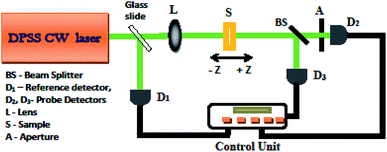 |
| | Fig. 1 Experimental Z-scan setup. | |
3. Results and discussions
3.1 Analysis of structural properties using X-ray diffraction
The structural properties of the prepared films were assessed by an X-ray diffractometer (XRD) having wavelength of 1.5406 Å through the precise range from 20° to 65°, as shown in Fig. 2(a). All peaks in the recorded XRD pattern were identified and indexed with JCPDS card number for ZnO – 00-001-1136 and for Co – 01-089-7373, which confirms the diffraction patterns corresponding to the planes (1 0 0), (0 0 2), (1 0 1), (1 0 2) and (1 0 0) were correctly indexed to the hexagonal wurtzite ZnO structure and it reveals that through Co-doping the crystal structure of the ZnO is unchanged, hence it implies that, there were no secondary phases such as Co clusters or oxides. All the prepared films exhibited preferential growth orientation along the (002) plane.37
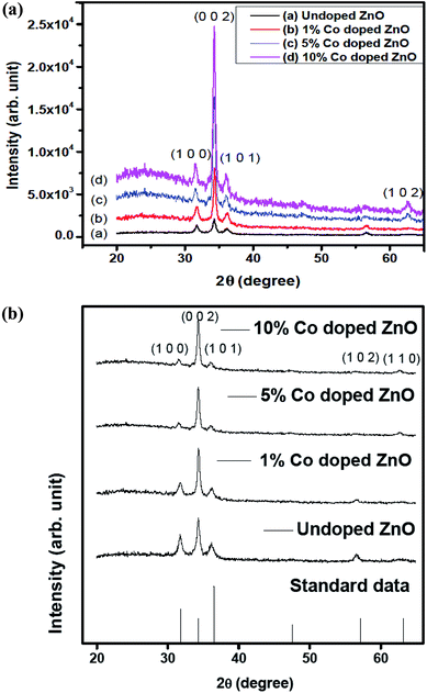 |
| | Fig. 2 (a) XRD patterns of undoped and Co-doped ZnO thin films. (b) JCPDS standard peaks. | |
It is observed from Fig. 2 that the intensity of the (0 0 2) peak increases with the Co concentration. We also detected a minimal shift in the position of the (0 0 2) diffraction peak toward lower values of the diffraction angle (2θ). The broad peak indicated the formation of a nanostructure. The crystallite size was calculated based on the width of the (0 0 2) peak, which appeared at 34.18° on the 2θ scale, using the Scherrer relation:38
| |
 | (1) |
Here,
Davg is the crystallite size,
θ is the Bragg's angle and
β is the full width at half maximum (FWHM), which is given in radians.
From the XRD observation, the lattice constants (a and c) and the inter-planar spacing (dhkl) were calculated using the following equations:39
| |
 | (2) |
Here,
d is the interplanar distance and
h,
k and
l are the Miller indices. The lattice constants
a and
c were calculated using the following equations:
| |
 | (3) |
| |
 | (4) |
It can be seen that the lattice constant (ao) decreases as the concentration of cobalt increases. We also estimated the dislocation density (δ) and lattice strain of the prepared films from the current structural studies using the following relation:40
| |
 | (5) |
Here,
n = 1, which indicates the lowest dislocation density of the film, and
D is the crystallite size. Usually, the number of dislocations per unit area determines the dislocation density of the film. These data show the quality of the films and defect states in a given material. In the current study, the dislocation density of the Zn
1−xCo
xO films decreased from 2.5860 × 10
15 m
−2 for pure films to 0.6090 × 10
15 m
−2 for 10 wt% Co-doped ZnO films, which indicated that Co incorporation in ZnO decreased the defects in the films. The lattice strain of the current thin films was also determined using the formula (
Table 2):
| |
 | (6) |
Table 2 XRD results for the structural parameters of Zn1−xCoxO thin films
| Samples (wt%) |
2θ (002) |
d(hkl) (Å) (±1%) |
Lattice parameters (Å) |
FWHM |
D (nm) (±2%) |
‘ε’ |
‘δ’ × 1015 (m−2) |
Roughness (nm) (±2%) |
| a |
c |
| 0% Co |
34.18 |
2.62 |
3.66 |
5.24 |
0.73 |
19.68 |
0.59 |
2.58 |
3.68 |
| 1% Co |
34.29 |
2.60 |
3.62 |
5.21 |
0.42 |
34.46 |
0.34 |
0.84 |
0.91 |
| 5% Co |
34.27 |
2.61 |
3.63 |
5.22 |
0.42 |
34.49 |
0.34 |
0.84 |
0.56 |
| 10% Co |
34.30 |
2.61 |
3.63 |
5.22 |
0.35 |
40.52 |
0.29 |
0.60 |
0.31 |
3.2 Morphological, elemental composition and surface topography studies
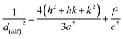
3.2.1 FESEM analysis. To analyze the microscopic characteristics of the prepared Zn1−xCoxO thin films, FESEM was used. The microscopic features have a substantial impact on the structural properties of the prepared thin films. Fig. 3(a–d) show the FESEM images of the Zn1−xCoxO thin films. The SEM data revealed a dense microstructure with flakes emerging from the surface. A closer examination revealed that there were pores in the film, which were randomly distributed. The films prepared with 5 and 10 wt% Co exhibited porous morphology and well-packed structures. The most drastic change occurred in the microstructure of 5 wt% Co-doped ZnO films. The ZnO thin film doped with 10 wt% of Co showed microstructures ranging from dense films to slightly porous microstructures, micro/nanorods and nanowires. However, the grain sizes of the thin films were enhanced with the increase in dopant (Co) concentration. This result agreed with the calculated XRD data. From these images it is observed that the formed transition metal doped ZnO films are highly yielded surface and the average sizes of the nanoparticles are 80–100 nm.
 |
| | Fig. 3 FESEM images of undoped and Co-doped ZnO thin films. | |
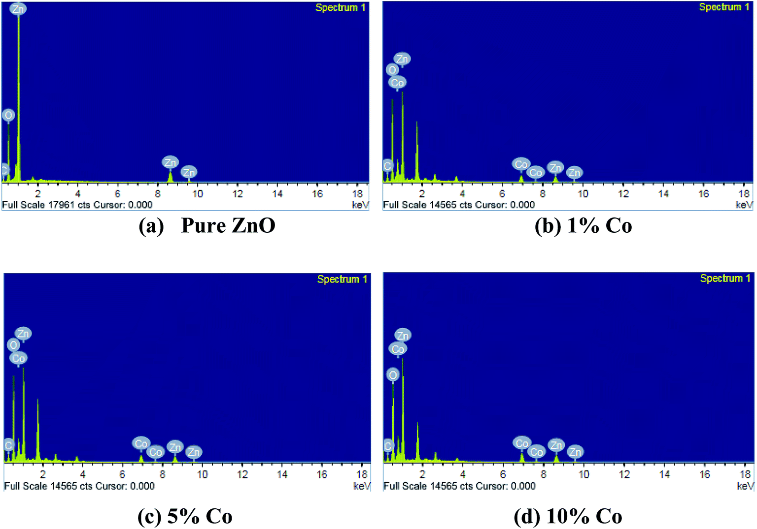
3.2.2 Energy dispersive X-ray analysis (EDAX). The elemental composition of the fabricated films was obtained using EDAX; the results are shown in Fig. 4. As expected, all the prepared films have the elements Zn, O and Co. The decreased O/Zn ratio attained for the coated films suggested that the films are marginally lacking in oxygen or have surplus zinc. At higher substrate temperatures, i.e., >300 °C, films with perfect stoichiometry were obtained. Also, with increased carrier concentration, the growth mechanism of the ZnO thin films improved.
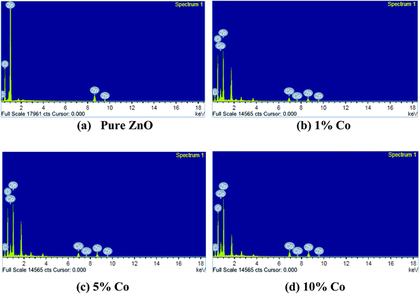 |
| | Fig. 4 EDAX images of undoped and Co-doped ZnO thin films. | |
3.2.3 Surface topography. The nanoscope software was used to calculate the roughness values of the prepared films. Fig. 5(a) shows the surface roughness of the prepared films. The results are in good agreement with the XRD results, showing a standard orientation, i.e., along the (0 0 2) plane. The formation of an island structure in the film increased the number of columnar grains in the 10 wt% Co-doped film. The surface roughness value of the prepared films decreased on increasing Co doping. The increase in Co doping usually results in the segregation of the secondary phase in the grain boundaries, thereby hindering the grain growth and deteriorating the crystal structure. Therefore, the grain growth was inhibited because of the decreased diffusivity, which in turn increased the grain size. As the grain size became larger, the surface roughness further decreased.
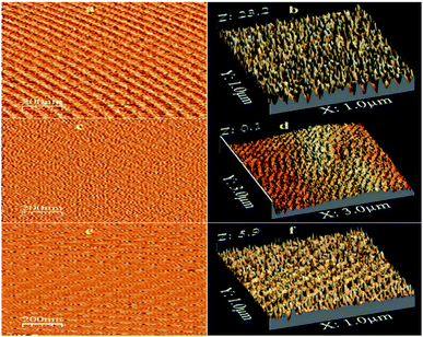 |
| | Fig. 5 AFM micrographs and surface roughness of undoped and Co-doped ZnO films elaborated at different doping concentrations: (a and b) pure ZnO, (c and d) 1% Co and (e and f) 10% Co. | |
3.3 Optical properties
To study the nature of the electronic transitions for the as-grown ZnO thin films, the optical absorption spectra for all the deposited films were recorded in the range of 300–800 nm using a UV-visible double-beam spectrophotometer, as shown in Fig. 6. To obtain detailed information about the Eg values of the films, the dependence of the absorption coefficient (α) on the photon energy (E) in the high absorption region was analyzed. The results showed that the undoped film exhibited transmittance of 70% for wavelengths longer than 500 nm. Furthermore, small absorption bands can be noticed in the range of 590–690 nm for the Co-doped ZnO samples. The absolute strength of these absorption bands increased almost linearly with the increase in Co concentration. Since the ionic radius of Co2+ (72 pm) is similar to that of Zn2+ (74 pm) in the tetrahedrally coordinated structure, this phenomenon can be attributed to the d–d transitions of the tetrahedrally coordinated Co2+.41 These transitions cause change in the sample color from white to green.
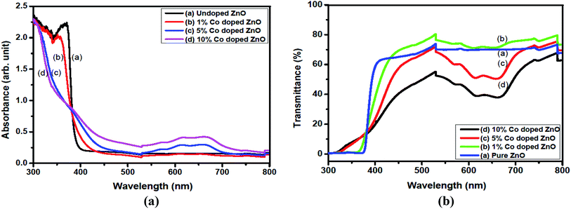 |
| | Fig. 6 UV-visible spectra for (a) absorbance (ar.u.) and (b) transmittance vs. wavelength for the undoped and Co-doped ZnO thin films. | |
The spectrum shows high transmittance in the visible and infrared regions and low transmittance in the ultraviolet region. The maximum transmittance observed was about 95% for the undoped ZnO sample. The absorbance decayed rapidly at shorter wavelengths corresponding to the band-gap of the prepared films. The energy band-gap of a material increases because of the interaction of the electrons in accordance with the input photon energy. The higher concentrations increasing the band gap which can be attributed due to increasing the electron concentration is providing more energy by photon to jump from valance band to conduction band. The absorption coefficient (α) values of the prepared thin films at different doping levels of Co were >104 cm−1, which implied the increase in probability of the occurrence of direct transitions. The energy band-gap was calculated using the following relation:42
Here,
A is a constant,
α is the absorption coefficient, and
N is a constant equal to 2 for an indirect transition and 0.5 for a direct transition. The (
αhγ)
2 values against photon energy are represented in
Fig. 7. An optical direct energy band-gap (
Eg) values were found to be 3.21, 3.25, 3.41 and 3.45 eV for the Zn
1−xCo
xO films with
x = 0, 1, 5 & 10 wt% of Co, respectively. It was noticed that the
Eg value increased with the increase in doping (Co) concentration.
 |
| | Fig. 7 (αhν)2 vs. photon energy for undoped and Co-doped ZnO thin films. | |
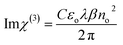
3.4 Third-order NLO properties
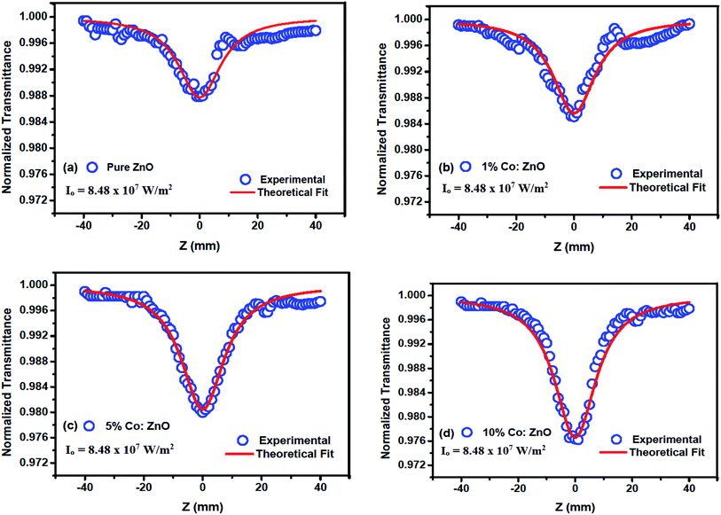
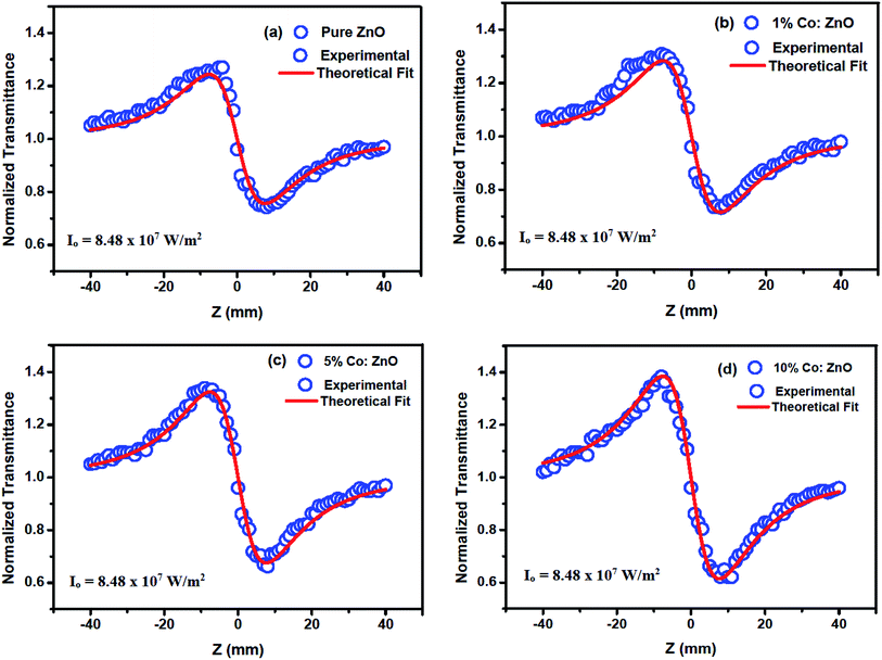
A high-intensity laser radiation incident on a thin film material causes special phenomena such as second- and third-order NLO effects. These effects are due to the interaction of induced polarization (p) with an applied electric field (E). The interaction is a linear function at a low intensity, which provides linear optical effects, and they produce a nonlinear function at a high intensity. The nonlinear electronic polarizability (PNL) is determined using the following equation:Here, PNL = χ(2)E + χ(3)E and it is the nonlinear polarizability; χ(1), χ(2) and χ(3) are the linear, second, and third-order NLO susceptibilities, respectively. To estimate the intensity dependency of the nonlinear absorption and nonlinear refraction processes for the thin films, OA and CA Z-scan experiments were carried out at an input intensity of 8.48 × 10⁷ W m−2.43 Fig. 8 illustrates the open aperture measurements for the Co-doped thin films. For each z position, the sample will see a different laser density and the sample transmission for different z position is measured using a laser energy meter. Many organic and inorganic samples show a change over from saturable absorption (SA) to reverse saturable absorption (RSA) and vice versa.44
 |
| | Fig. 8 Open-aperture Z-scan traces for undoped and Co-doped ZnO thin films. | |
3.4.1 Nonlinear absorption. The nonlinear absorption coefficient (β) was determined from the OA Z-scan measurements. The recorded open aperture pattern clearly demonstrates that all materials display nonlinear absorption, and the inverse saturable absorption-type behavior is due to maximum transmittance at the focus. As the sample is moved away from the source, the normalized transmittance increases with respect to the focus (Z = 0) and then, it is reduced as the sample moves closer to the source. When the sample is far from the beam waist, no transmission change is evident. A nearly linear rise in transmission from the wing to peak is noted in the experimental information. A similar pattern of linear increase in transmittance from the wing to the peak is noted under comparable experimental conditions for other materials.45 The reason for this may not be due to the nature of the material alone (scattering problems), but it may also be due to the laser spatial quality. In order to obtain a clear image of the transmittance from the peak to wing region, a thorough inquiry must be carried out by minimizing the Z-position interval and repeating the experiment.With reference to the focus (z = 0), the transmission is symmetric and minimal. The presence of valleys in the OA scan indicates strong RSA.46 To confirm the observed nonlinearity and estimate the nonlinear absorption (β) coefficient, the experimental OA data (represented as scattered circles) were theoretically fitted (solid line) using the raw data. The 2PA coefficient (β) was calculated using the following relation:45
| |
 | (9) |
Here,

is a beam waist;
is the effective thickness of the sample;

is the linear absorption coefficient at a wavelength of 532 nm;
d is the sample length;
Io is the intensity of the laser beam; and
β is the NLA coefficient.
Fig. 8 depicts the relationship of the normalized transmittance
T to the distance (
z/
zo) for different Co-doped ZnO films. The obtained NLA coefficient (
β) values are shown in
Table 3. The nonlinear absorption coefficient of the films apparently increased with the increase in doping concentration. However, as CW lasers were used as a source of excitation in the current situation, the source of nonlinearity was solely thermal, and the sample acted as a thermal lens.
47 Thus, the nonlinear absorption observed is anticipated from the open aperture pattern signature, which is of reverse saturable absorption type in the current situation. Here, multi-photon processes cannot explain the source of nonlinearity as CW lasers generate weak electronic effects and the original nonlinearity is solely due to thermal effects.
Table 3 Third-order NLO parameters of Zn1−xCoxO thin films
| Composition of Co |
NLA coefficient (β) × 10−3 cm W−1 (±2%) |
NLR index (n2) × 10−8 cm2 W−1 (±2%) |
Real part of NLO susceptibility × 10−6 (χR(3)) esu |
Imaginary part of NLO susceptibility × 10−7 (χimg(3)) esu |
Third-order NLO susceptibility (χ3) × 10−6 esu (±5%) |
| Pure ZnO |
4.68 |
−1.37 |
0.78 |
0.12 |
0.79 |
| 1% Co |
5.31 |
−1.54 |
0.88 |
0.13 |
0.89 |
| 5% Co |
7.53 |
−1.94 |
1.35 |
0.18 |
1.36 |
| 10% Co |
9.92 |
−2.90 |
1.87 |
0.24 |
1.88 |
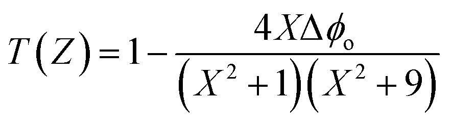
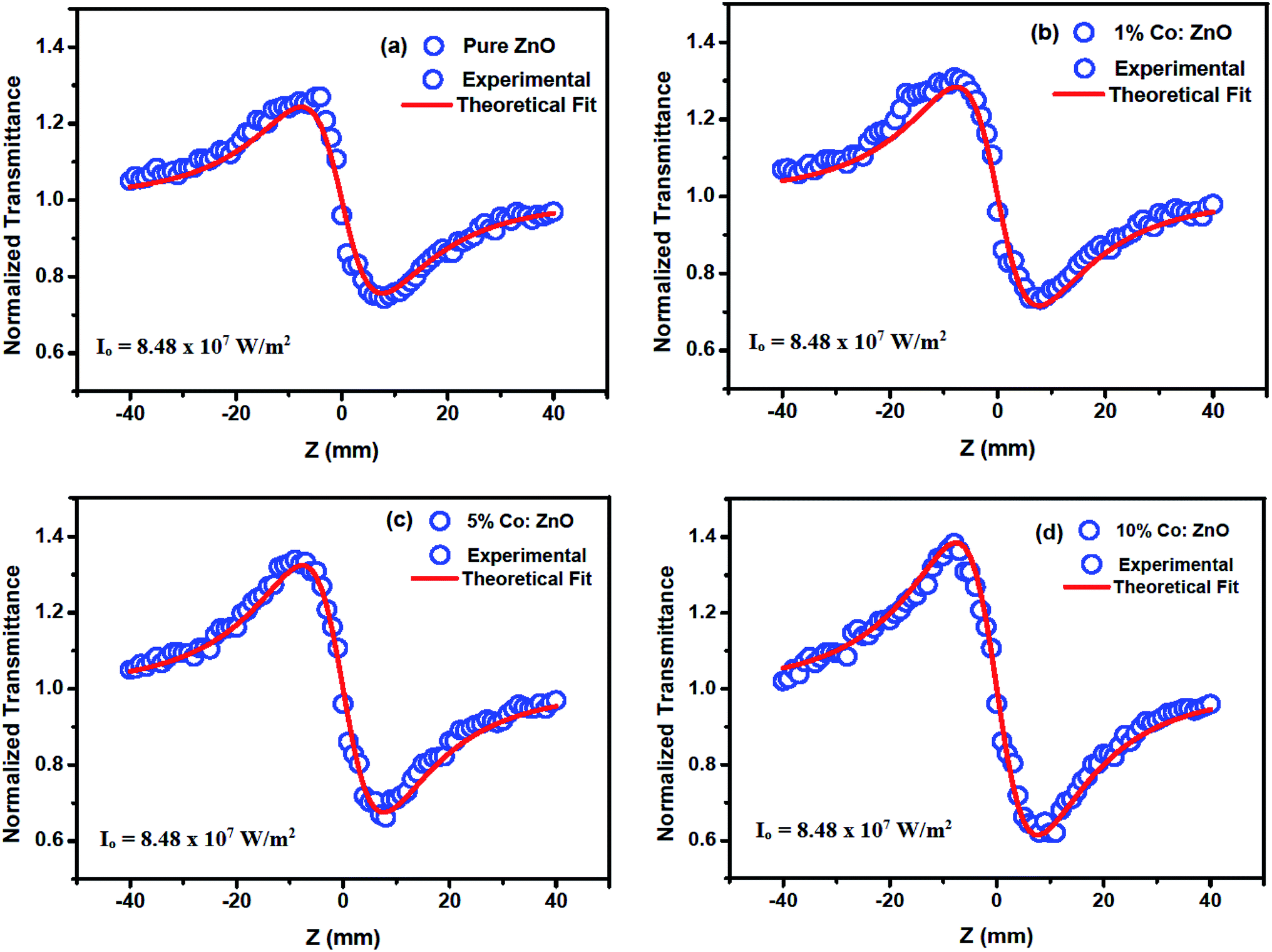
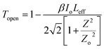
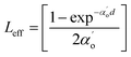
3.4.2 Nonlinear refractive index. The nonlinear refractive index (n2) of pure and Co-doped films was determined using the CA Z-scan technique.48 The aperture was kept at the front of the detector and allowed us to find the sign and also the magnitude n2 of all Co-doped ZnO films. In the input intensity spectrum engaged in the studies, closed aperture traces could be reproduced and demonstrated the existence of a powerful nonlinear refractive behavior. The nonlinear refractive behavior of the sample under CW laser excitation is equal to the creation of an induced positive or negative lens, resulting in a self-focusing or self-defocusing behavior. The nonlinear response from the sample was obviously noticeable with the distance during the measurement, shown by an intensive self-focused disk when the sample was nearer to the lens and the laser source on the side and as a self-defocused optical vortex when the sample was on the opposite side of the focal point. The recorded normalized closed aperture Z-scans display a pre-focal peak, followed by a post-focal valley, showing the adverse nonlinearity of the sample and the defocusing lensing impact (negative nonlinear refraction). This may be due to the thermal nonlinearity resulting from the absorption of radiation at 532 nm. In the closed aperture pattern, the scattered circles represent the experimental data, and the solid line is the theoretical fit, as proposed by Sheik-Bahae. The closed aperture results are shown in Fig. 9. Using the results of n2 and βeff, the NLO susceptibility χ(3) was determined by the following equations.49 First, to determine the phase shift (Δϕo), the experimental CA data were fitted theoretically using the following equation:| |
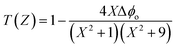 | (10) |
Here, x = z/zo. With the Δϕo value obtained from the relation Δϕo = Kn2IoLeff, the nonlinear refractive index (n2) was calculated. The real part of the third-order NLO susceptibility was determined through the following equation:
 |
| | Fig. 9 Closed-aperture Z-scan plots for undoped and Co-doped ZnO thin films. | |
The imaginary part of the third-order NLO susceptibility was determined using the following relation:
| |
 | (12) |
Using the above results, the magnitude of NLO susceptibility was expressed using the following equation:50
| | |
|χ(3)| = |Reχ(3) + iImχ(3)|
| (13) |
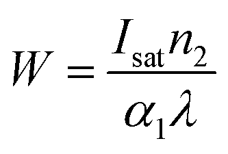
The third-order NLO properties are shown in Table 3. The increasing behavior can be explained in terms of the improvement in crystallinity with the Co doping concentration. Optical nonlinearity also increased at higher Co concentrations due to the increase in carrier concentration. The structural properties and surface roughness are the key factors for the scattering of light intensity for films and generate the highest NLO response. We conducted a Z-scan experiment on the plain glass slides used and found negligible contributions for both nonlinear refraction and nonlinear absorption at the input intensity used. Therefore, at the input intensity used, any contribution from the plane glass slide to the observed nonlinearity is negligible. Continuous wave (CW) lasers having powers ranging from μW to kW are widely used in various applications.51 This necessitates the need for protecting optical sensors and human eyes from the high-intensity laser beams. The factors like the nonlinear absorption figure of merits ‘W’ (FOM) for all the prepared thin films were studied and evaluated using the following equation:
| |
 | (14) |
Where,
Isat is the intensity of light to which the NRI is subjected. FOM depends on the value of the nonlinear refractive index and increases with the doping concentration. For useful optical device applications, the value of ‘
W’ must be greater than one.
52 In the current Co-doped ZnO films, the value of
W was found to be nearly 1. It was also noted that the number of clusters interacting with the laser beam increased with decrease in the crystallite size, which eventually led to an increase in the nonlinear optical susceptibility and hyperpolarizability. The peak-valley patterns obtained under the closed aperture configuration of the normalized transmittance curve reveal the self-defocusing behavior of the propagation in the samples, a property with wide applications for protecting the optical sensor. The recorded NRI (
n2) value was high for all these doped films compared to those of some previously reported materials of interest.
30 However, the actual potency of these materials was strongly dependent on
n2 for optical switching-based applications. The change in refractive index, as indicated by the thermo-optic effect,
35 occurred because of the higher thermal contribution of the non-radiative relaxation of the excited levels, which caused phase changes in the material. Optical nonlinearity is temperature-dependent, and the outcome rise in third-order nonlinearity. In the present case, nonlinearity was thermal in nature because a CW laser was used. The peak-to-valley (
TP-V) separation was approximately twice the Rayleigh range (
ZR) of the laser used. We believe that nonlinear scattering is the reason for the minor deviations of the theoretical fit to the experimental data. When the medium is illuminated by a laser, at higher doping concentrations, a large number of particles are thermally agitated because of the local heating of the absorbing medium, resulting in temperature variation in the sample medium.
53
3.5 Optical limiting studies
Over the past few years, studies on materials with optical limiting behaviors have focused on nonlinear inorganic materials, and this is usually due to the nonlinear absorption of the molecules. The critical power of the laser beam at which nonlinearity begins to influence transmission can be assessed by an optical limiting procedure. For weak optical signals, a device must show very high transmission and become opaque for large optical signals.54 Currently, much interest is being directed toward the search for novel NLO materials for optical limiters that can be used to protect solid-state optical sensors and optical devices exposed to intense laser beams. OL or optical restricting is a phenomenon detected when the transmission of a medium decays with the increasing input power of the laser. A successful optical limiter will have a low restricting threshold, stability, a fast response time, optical clarity and high linear transmittance throughout the sensor bandwidth. OL can be accomplished through numerous NLO mechanisms such as MPA, free carrier absorption (FCA), nonlinear scattering, excited state absorption (ESA), self-focusing, and self-defocusing. Also, the optical limiting response was found to increase with decreasing crystallite size in our investigations. This is because the divergence angle due to self-defocusing and absorbance decreases with the decrease in the crystallite size, thereby increasing the clamping value.55
The source used to probe a nonlinear material is a CW laser. Fig. 10 shows a typical OL curve concerning the input fluence. It is obvious that the curve departs under strong irradiance from the Lambert–Beer's law, leading to OPL in the thin film. The Gaussian beam input intensity profiles at different positions (z/zo) were assessed, and the transmitted power through the prepared films at each (z/zo) position was recorded.56 The OL threshold values of undoped ZnO and 1, 5 and 10 wt% Co-doped ZnO were found to be 7.8, 5.8, 2.8 and 2.1 kJ cm−2, respectively. Thus, the fabricated films are stimulating materials for all-optical switching devices. The result of our article are in excellent agreement with some previously reported NLO of ZnO materials; also, the magnitude of the third-order NLO susceptibilities is at least one order higher compared to that reported in ref. 57. In our current material, it was confirmed that the crystalline quality of the films is the key factor for the large NLO properties. Under CW laser excitation, the thermal effect will enhance ESA, indicating that ESA-assisted RSA is the NLO mechanism responsible for the OL behavior of the prepared Zn1−xCoxO films.58
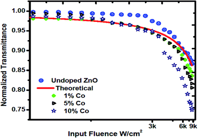 |
| | Fig. 10 Optical power limiting response of the fabricated undoped and Co-doped ZnO films. | |
4. Conclusion
To sum up, thin films of undoped and Co-doped ZnO were prepared by the spray pyrolysis technique. The strong influence of Co doping in the ZnO thin films on the structure and morphology was observed, and the enhancement in linear optical and third-order NLO properties was found. The XRD patterns showed an excellent crystalline behavior with the hexagonal wurtzite structure with preferential growth along the (0 0 2) plane. The FESEM images showed that the prepared films have uniform surface coverage over the substrate. The elemental composition of the fabricated films was obtained by recording EDAX spectra; as expected, the elements Zn, O and Co were found. The surface roughness of all the films was found to decrease with the increase in Co doping. The thin films were optically transparent in the vis-NIR region and possessed a direct band gap, which was found to increase with the increase in doping percentages. The Z-scan OA studies demonstrated a strong nonlinear absorption behavior (β ∼ 10−3 cm W−1) for the doped thin films. All the samples were found to possess enhanced NRI (n2 ∼ 10−8 cm2 W−1) and third-order NLO susceptibility (χ(3) = 10−6 esu) values. Open aperture Z-scan curves indicated a reverse saturable absorption behavior, and the closed aperture curves showed negative nonlinear refractions. Large phase shifts were observed due to the thermal contribution from the CW laser. The Z-scan studies reflected the negative nonlinearity of the samples; hence, the self-defocusing nature was responsible for the optical limiting behavior in the regime of interest. These encouraging NLO and optical limiting threshold results indicate that the transition-metal Co-doped ZnO thin films can be used in photonic devices and as optical limiters.
Conflicts of interest
All authors declare no conflict of interest.
Acknowledgements
The author Raghavendra Bairy would like to express thanks to NMAM Institute of Technology, Nitte, India for providing the research facilities and encouragement to carry out the study. Authors are grateful to Mangalore University, DST-PURSE laboratory and the Department of Physics, KLE college of Engineering Hubballi.
References
- A. Manzoli, M. Santos and S. Machado, Thin Solid Films, 2007, 515, 6860–6866 CrossRef CAS.
- H. Zhang, H. Liu and C. Lei, et al., J. Semiconductors, 2010, 31(8), 083005 CrossRef.
- G. Rusu, V. Ciupina, M. Popa, G. Prodan, G. Rusu and C. Baban, J. Non-Cryst. Solids, 2006, 352, 1525–1528 CrossRef CAS.
- K. Ip, R. M. Frazier, Y. W. Heo, D. P. Norton, C. R. Abernathy, S. J. Pearton, J. Kelly, R. Rairigh, A. F. Hebard, J. M. Zavada and R. G. Wilson, J. Vac. Sci. Technol., B: Microelectron. Nanometer Struct.--Process., Meas., Phenom., 2003, 21, 1476–1481 CrossRef CAS.
- D. Bao, H. Gu and A. Kuang, Thin Solid Films, 1998, 312, 37–39 CrossRef CAS.
- S. Fujihara, C. Sasaki and T. Kimura, Appl. Surf. Sci., 2001, 180, 341–350 CrossRef CAS.
- J. H. Lee, P. Lin, J. C. Ho and C. C. Lee, Electrochem. Solid-State Lett., 2006, 9, G117–G120 CrossRef CAS.
- F. K. Allah, S. Y. Abé, C. Núñez, A. Khelil, L. Cattin, M. Morsli, J. Bernède, A. Bougrine, M. Del Valle and F. Díaz, Appl. Surf. Sci., 2007, 253, 9241–9247 CrossRef CAS.
- T. Anto Johny, V. Kumar, P. Sudheesh and K. Chandrasekharan, Opt. Commun., 2013, 279–281, 309 Search PubMed.
- M. A. Lamrani, M. Addou, Z. Sofiani, B. Sahraoui, J. Ebothe, A. El Hichou, N. Fellahi, J. Bernede and R. Dounia, Opt. Commun., 2007, 277, 196–201 CrossRef CAS.
- V. Ganesh, I. S. Yahia, S. AlFaify and M. Shkir, J. Phys. Chem. Solids, 2017, 100, 115–125 CrossRef CAS.
- E. R. Shaaban, M. El-Hagary, E. S. Moustafa, H. Shokry Hassan, Y. A. M. Ismail, M. Emam-Ismail and A. S. Ali, Appl. Phys. A, 2016, 20, 122 Search PubMed.
- S. J. Pearton, D. P. Norton, K. Ip, Y. W. Heo and T. Steiner, J. Vac. Sci. Technol., B: Microelectron. Nanometer Struct.--Process., Meas., Phenom., 2004, 22, 932–948 CrossRef CAS.
- L. Jiang, X. Tan, T. Xiao, P. Xiang and J. Li, J. Alloys Compd., 2017, 718, 116–121 CrossRef CAS.
- A. Singh, S. Schipmann, A. Mathur, D. Pal, A. Sengupta, U. Klemradt and S. Chattopadhyay, Appl. Surf. Sci., 2017, 414, 114–123 CrossRef CAS.
- L. Duta, N. Mihailescu, A. C. Popescu, C. R. Luculescu, I. N. Mihailescu, G. Cetin, O. Gunduz, F. N. Oktar, A. C. Popa, A. Kuncser, C. Besleaga and G. E. Stan, Appl. Surf. Sci., 2017, 413, 129–139 CrossRef CAS.
- H. Wang, M. Wei, Z. Zhong and Y. Wang, J. Membr. Sci., 2017, 535, 56–62 CrossRef CAS.
- A. R. Khantoul, M. Sebais, B. Rahal, B. Boudine and O. Halimi, Acta Phys. Pol., A, 2018, 133, 114–117 CrossRef CAS.
- S.
L. Kwon, Y. U. Jin, B. J. Kim, M. H. Han, G. S. Han, S. Shin, S. Lee and H. S. Jung, Appl. Surf. Sci., 2017, 416, 96–102 CrossRef CAS.
- S. Abed, M. S. Aida, K. Bouchouit, A. Arbaoui, K. Iliopoulos and B. Sahraoui, Opt. Mater., 2011, 33, 968–972 CrossRef CAS.
- K. Bahedi, M. Addou, M. El Jouad, Z. Sofiani, M. A. Lamrani, T. El Habbani, N. Fellahi, S. Bayoud, L. Dghoughi, B. Sahraoui and Z. Essaidi, Appl. Surf. Sci., 2009, 255, 4693–4695 CrossRef CAS.
- Z. Sofiani, B. Sahraoui, M. Addou, R. Adhiri, M. A. Lamrani, L. Dghoughi, N. Fellahi, B. Derkowska and W. Bala, J. Appl. Phys., 2007, 101, 063104 CrossRef.
- M. A. Lamrani, M. Addou, Z. Sofiani, B. Sahraoui, B. Sahraoui, J. Ebothe, A. El Hichou, N. Fellahi, J. C. Bernede and R. Dounia, Opt. Commun., 2007, 277, 196–201 CrossRef CAS.
- Z. Sofiani, B. Derkowska, P. Dalasiski, M. Wojdyla, S. D. Seignon, M. A. Lamrani, L. Dghoughi, W. Bala, M. Addou and B. Sahraoui, Opt. Commun., 2006, 267, 433–439 CrossRef CAS.
- O. G. M. Saavedra, L. Castaneda, J. G. Banuelos and R. O. Martinez, Laser Phys., 2008, 18, 283–291 CrossRef.
- Y. Teng-Fei, L. Ying, K. Jun-Jie, Z. Peng-Yu, S. Bao-Quan, Z. Kun, Y. Shi-Shen and Z. Xin-Hui, Chin. Phys. Lett., 2015, 32(7), 077801 CrossRef.
- L. Irimpan, A. Deepthy, B. Krishnan, L. M. Kukreja, V. P. N. Nampoori and P. Radhakrishnan, Opt. Commun., 2008, 281, 2938–2943 CrossRef CAS.
- G. P. Bharti and A. Khare, Opt. Mater. Express, 2016, 6, 2063 CrossRef CAS.
- M. A. Lamrani, M. Addou, Z. Sofiani, B. Sahraoui, J. Ebothe, A. El Hichou, N. Fellahi, J. Bernede and R. Dounia, Opt. Commun., 2007, 277, 196–201 CrossRef CAS.
- S. Abed, M. S. Aida, K. Bouchouit, A. Arbaoui, K. Iliopoulos and B. Sahraoui, Opt. Mater., 2011, 33, 968–972 CrossRef CAS.
- R. Vinodkumar, I. Navas, S. R. Chalana, K. G. Gopchandran, V. Ganesan, R. Philip, S. K. Sudheer and V. P. M. Pillai, Appl. Surf. Sci., 2010, 257, 708–716 CrossRef CAS.
- K. C. Sanal, V. Shijeesh and M. K. Jayaraj, Proc. SPIE, 2016, 9161, 91611B Search PubMed.
- X.-Y. Yan, C.-B. Yao, J. Li, J.-Y. Hu, Q.-H. Li and S.-B. Yang, Opt. Mater., 2016, 55, 73–77 CrossRef CAS.
- Y. Caglar, J. Alloys Compd., 2013, 560, 181–188 CrossRef CAS.
- M. Saravanan, T. C. Sabari Girisun and G. Vinitha, J. Mater. Sci.: Mater. Electron., 2015, 1–8 Search PubMed.
- M. Sheik-Bahae, A. A. Said, T. H. Wei, D. J. Hagan and E. W. Van Stryland, IEEE J. Quantum Electron., 1990, 26, 760 CrossRef CAS.
- M. Miki-Yoshida, J. Morales and J. Solis, Thin Solid Films, 2000, 373, 137–140 CrossRef.
- B. Cullity, Elements of X-Ray Diffraction, Addison-Wesley Pub. Co, Inc., CA, USA, 2nd edn, 1978, p. 356 Search PubMed.
- C. M. Muiva, T. S. Sathiaraj and K. Maabong, Ceram. Int., 2011, 37, 555–560 CrossRef CAS.
- K. Usha, R. Sivakumar and C. Sanjeeviraja, J. Appl. Phys., 2013, 114, 123501 CrossRef.
- K. J. Kim and Y. R. Park, J. Appl. Phys., 2003, 94, 867–869 CrossRef CAS.
- J. Tauc, Amorphous and Liquid Semiconductors, Plenum Press, New York, 1974, p. 159 Search PubMed.
- Z. S. Fadhul, E. A. H. F. Ali, S. R. Maidur, P. S. Patil, M. Shkir and F. Z. Henari, J. Nonlinear Opt. Phys. Mater., 2018, 27, 1850012 CrossRef CAS.
- B. Gananatha Shetty, V. Crasta, N. B. Rithin Kumar, K. Rajesh, R. Bairy and P. S. Patil, Opt. Mater., 2019, 95, 109218 CrossRef.
- T. Geethakrishnan and P. K. Palanisamy, Z-scan determination of the third-order optical nonlinearity of a triphenylmethane dye using 633 nm He–Ne laser, Opt. Commun., 2007, 270, 424–428 CrossRef CAS.
- B. G. Shetty, C. Vincent, N. B. Rithin Kumar, K. Rajesh and R. Bairy, Mater. Res. Express, 2019, 6, 1–14 Search PubMed.
- F. L. S. Cuppo, A. M. Figueiredo Neto, S. L. Go'mez and P. Palffy-Muhoray, Thermal-lens model compared with the Sheik-Bahae formalism in interpreting Z-scan experiments on lyotropic liquid crystals, J. Opt. Soc. Am. B, 2002, 19(6), 1342 CrossRef CAS.
- D. Haleshappa, A. Jayarama, R. Bairy, S. Acharya and P. S. Patil, Phys. B, 2019, 555, 125–132 CrossRef CAS.
- R. Bairy, A. Jayarama, G. K. Shivakumar, S. D. Kulkarni, S. R. Maidur and P. S. Patil, Phys. B, 2019, 555, 145–151 CrossRef CAS.
- M. Sheik-Bahae, A. A. Said, T. Wei, D. J. Hagen and E. W. Van Stryland, IEEE J. Quantum Electron., 1990, 26, 760 CrossRef CAS.
- C. Gayathri and A. Ramalingam, Spectrochim. Acta A, 2008, 69, 980–984 CrossRef CAS.
- R. Bairy, A. Jayarama, G. K. Shivakumar, K. Radhakrishnan and U. K. Bhat, J. Mater. Sci.: Mater. Electron., 2019, 30, 6993–7004 CrossRef CAS.
- C. Babeela and T. C. Sabari Girisun, Opt. Mater., 2015, 49, 190–195 CrossRef CAS.
- S. Dhanuskodi, T. C. Sabari Girisun and S. Vinitha, Curr. Appl. Phys., 2011, 11, 860–864 CrossRef.
- T. C. Sabari Girisun and S. Dhanuskodi, Cryst. Res. Technol., 2009, 44, 1297–1302 CrossRef.
- N. Venkatram, D. Narayana Rao and M. A. Akundi, Opt. Express, 2005, 13, 867 CrossRef CAS.
- U. P. Shaik, P. Ajay Kumar, M. G. Krishna and S. Venugopal Rao, Mater. Res. Express, 2014, 1, 046201 CrossRef.
- T. C. Sabari Girisun, M. Saravanan and S. Venugopal Rao, J. Appl. Phys., 2018, 124, 193101 CrossRef.
|
| This journal is © The Royal Society of Chemistry 2019 |
Click here to see how this site uses Cookies. View our privacy policy here. 
 Open Access Article
 This Open Access Article is licensed under a Creative Commons Attribution-Non Commercial 3.0 Unported Licence
 *a,
Parutagouda shankaragouda Patil
*a,
Parutagouda shankaragouda Patil


 is a beam waist;
  is the effective thickness of the sample;
  is the linear absorption coefficient at a wavelength of 532 nm; d is the sample length; Io is the intensity of the laser beam; and β is the NLA coefficient. Fig. 8 depicts the relationship of the normalized transmittance T to the distance (z/zo) for different Co-doped ZnO films. The obtained NLA coefficient (β) values are shown in Table 3. The nonlinear absorption coefficient of the films apparently increased with the increase in doping concentration. However, as CW lasers were used as a source of excitation in the current situation, the source of nonlinearity was solely thermal, and the sample acted as a thermal lens.47 Thus, the nonlinear absorption observed is anticipated from the open aperture pattern signature, which is of reverse saturable absorption type in the current situation. Here, multi-photon processes cannot explain the source of nonlinearity as CW lasers generate weak electronic effects and the original nonlinearity is solely due to thermal effects.