
 Open Access Article
 This Open Access Article is licensed under a Creative Commons Attribution-Non Commercial 3.0 Unported Licence
Self-powered gas sensor based on SiNWs/ITO photodiode†
Dong Liua,
Qiaofen Chena,
Aimin Chenb and
Jianmin Wu *a
*a
aInstitute of Analytical System, Department of Chemistry, Zhejiang University, Hangzhou, 310058, China. E-mail: wjm-st1@zju.edu.cn
bCollege of Chemical Engineering, Zhejiang University of Technology, Hangzhou 310014, China
First published on 30th July 2019
Abstract
Silicon nanowires (SiNWs) with a large surface-to-volume ratio and a low reflectivity are exceedingly attractive building blocks for developing high performance light harvesting devices. Herein, a SiNW/ITO heterojunction was fabricated easily by just compressing the SiNWs and ITO electrode together with a suitable pressure. Under light illumination, the SiNWs/ITO with an optimized structure can generate more than 20 μA photocurrent at zero bias voltage. In the mean time, the photocurrent is very sensitive to NO2 infiltration into the forest of SiNWs and displays a non-linear relationship with the concentration of NO2 from 0 to 1000 ppb. In comparison with chemiresistive sensors based on SiNWs only, the sensitivity of the self-powered sensor was improved obviously, showing a limit of detection at ∼5 ppb. The excellent light trapping and sensing performance was attributed to the heterojunction formed between SiNWs and ITO. Since the nano-photodiode device can monitor the surrounding gas without an external power supply, it will ensure that sensor networks can operate independently and sustainably without a battery or at least by extending the life time of a battery. This work may push forward the development of self-powered microsensors using rationally designed nanojunctions.
Introduction
A notable technological trend in today's society is the growing use of mobile and wireless electronic sensors in daily life.1–3 Various sensors can be applied in health care, medical monitoring, infrastructure/environment monitoring and product tracking within the world of the internet of things (IoTs).4 So developing multi-functional sensors which are ultra-small in size, super sensitive, multi-functional, and have extremely low power consumption is very important.5 Among them, powering wireless sensors during long-term operation periods without frequently replacing the power source has become a huge challenge.6 Self-powered sensor networks are likely to play key roles in the next few decades in driving the world economy.7 “Self-powered nanotechnology” could ensure that sensor networks can operate independently and sustainably without a battery or at least by extending the life time of a battery.8 Thus developing self-powered nanodevices and nanosystems without using batteries is of critical importance, for it can greatly enhance the nanodevices' adaptability and mobility. Therefore, there is an urgent need to develop nanomaterials and nanofabrication technologies that can harvest energy from the environment to self-power these nanodevices.9Up to now, the self-powered nanosystem known as an active sensor, has been achieved by using piezoelectric nanogenerators as either a power source or sensing signal in response to the change in environment, such as self-powered wind-velocity detectors, automobile speedometers, gas sensors, and magnetic sensors.10–13 The solar driven self-power sensor is another kind of promising strategy, which uses a multifunctional heterostructure to harvest solar light for driving the sensor in one hand and providing good sensing properties on another hand.14
Silicon nanowire (SiNW) arrays with their unique one-dimensional aligned structure and outstanding electrical properties,15 have attracted much attention because they are important photoelectric conversion materials with high optical absorption ability. For example, large-area ordered SiNW arrays prepared by electroless etching could intensively suppress light reflection over a wide spectral range from 300 to 1000 nm.16 The remarkable antireflection ability of the SiNW arrays has a great advantage over other texturized Si and other types of antireflection coating materials.17 More importantly, various types of heterojunctions and homojunctions can be constructed from SiNWs with different doping types and doping levels.18 A few recent studies have also implemented self-powered devices which are activated by light based on a p–n junction.19,20 The existing built-in electric field (BEF) can separate photogenerated carriers which facilitates the driving of devices under light illumination. For example, Hoffmann et al.21,22 reported two kinds of self-powered gas sensors using n-ZnO/p-Si and CdS@n-ZnO/p-Si, respectively. Yi Jia et al. utilize SiNW arrays to fabricate heterojunction with CNT membranes, which combines the functions of solar cell and gas sensor.23
In the present work, p-SiNWs and n-ITO were employed to fabricate the self-powered gas sensor with a simple p–n heterojunction structure which was activated by a light source. In this structure, the large specific surface area of SiNW arrays can greatly facilitate gas adsorption and desorption, further improving the sensing performances. Compared with the conventional chemiresistive gas sensor using SiNWs, the sensor reported here was capable of detecting NO2 concentrations at the sub-ppm level with a very high selectivity at room temperature (RT) and show a linear response to 50–1000 ppb NO2 when illuminated under visible light (λ = 576 nm, P = 20 mW cm−2). More importantly, the sensor can generate responding signal without need of an external power-source. The current results could stimulate a feasible approach for the next generation of portable low-temperature self-powered gas sensors.
Results and discussion
The schematic experimental setup is illustrated in Fig. 1. The SiNWs/ITO structure is basically constructed by compressing the transparent ITO and the tip of SiNWs with proper pressure. Such a structure allows sunlight to pass towards the SiNWs array. In order to investigate the performance of gas sensing, the SiNWs/ITO sensor was sealed into a chamber with a window for light illumination. The concentration of NO2 gas sample was adjusted by mixing the standard NO2 sample (16.8 ppm) with N2 at a specific ratio controlled by an automatic gas mixing apparatus. The sealed chamber was kept at room temperature. The current–voltage (I–V) data of SiNW/ITO heterojunction were recorded by a Keithley 6487 digital source-meter. | ||
| Fig. 1 Schematic diagram of the p-SiNW/ITO structure, the inset shows details of the heterojunction fabrication. | ||
The top view of SiNWs with low magnification shows that the as prepared SiNWs display high density and highly ordered structure over a large area (Fig. 2a). The cross-sectional view (Fig. 2b) indicates that semi-densely distributed SiNWs are oriented and vertical to the Si wafer substrate. The average length of the SiNWs prepared by 2 h electroless etching is about 37.5 μm and the diameters of SiNWs range from 50 to 200 nm. Minor broken SiNWs were caused by cutting and loading of the SEM specimens. With the increase of the etching time, the length of SiNWs increased linearly (Fig. S1†).
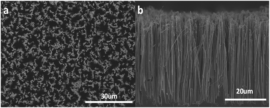 | ||
| Fig. 2 (a) Top view and (b) cross-sectional view SEM images of a SiNW arrays, the etching time was 2 h. | ||
Current–voltage (I–V) characteristics of the n-SiNWs/ITO device shows a symmetrical current response under both forward and reverse voltage scanning, even though a non-linear current response was observed owing to the formation of homojunction. Under light illumination, the n-SiNWs/ITO still displayed a symmetrical I–V curve (Fig. 3a). As shown in the zoomed in area ranging from −0.6 V to 0.6 V (Fig. 3b), the n-SiNWs/ITO cannot generate photocurrent at zero bias voltage, indicating that these kinds of structure cannot act as a self-powered device. In contrast, the I–V characteristics of p-SiNWs/ITO in dark and under illumination in nitrogen atmosphere show a significant rectifying effect (Fig. 3c), which was originated from the heterojunction at the p-SiNWs/ITO interface. In dark conditions, p-SiNWs/ITO showed typical rectifying diode behavior, while light illumination shifts the device characteristics to a photovoltaic effect. On the p-SiNWs/ITO heterojunctions, the current observed at light irradiation was significantly larger than that under dark condition when a negative voltage was applied, indicating the generation of photoexcited charge carriers at the heterojunctions. Even at zero voltage, a large photocurrent (>20 μA) was observed (Fig. 3d). Under positive voltage, the current response at light irradiation was only slightly larger than that at dark condition, indicating that negative voltages applied to the heterojunctions favour the generation of photocurrent. The phenomenon is in accordance with conventional semiconductor photodiode, which display a directional photocurrent response. Therefore, the p-SiNWs/ITO device was chosen as the self-powered device for gas sensing. Meanwhile, the photocurrent produced by this structure can sustain for a long time (Fig. S2†).
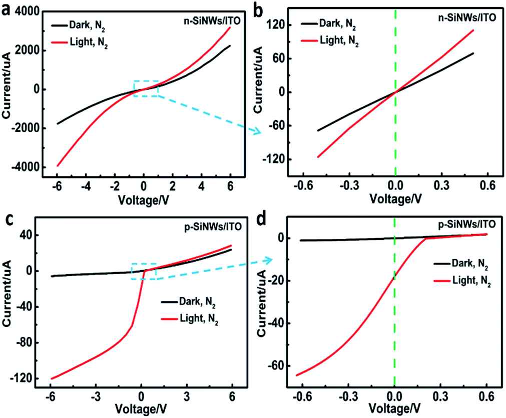 | ||
| Fig. 3 The current–voltage (I–V) curve of SiNWs/ITO heterojunction (a) n-type and (c) p-type SiNWs under dark (black) and visual LED (red) conditions and (b), (d) the amplification of (a), (c) respectively under N2 atmosphere, the etching time of SiNWs was 2 h. | ||
The device exhibited different photoresponse when the SiNWs length varied (Fig. 4a–d). The length of SiNWs was controlled by the etching time since the length of SiNWs have a proportional relationship with the etching time. In the present work, the etching time was set at 30 min, 1 h, 1.5 h, 2 h and 3 h, respectively. SEM indicated that the length of SiNWs increased with the increasing etching time (Fig. S1†). The I–V curves of SiNWs/ITO heterojunction with different SiNWs length in the dark and illumination indicated that the photoresponse increased with the increasing etching time from 0 to 2 h (Fig. 4a and b), but decreased when the etching time exceeded 2 h. The photocurrent of SiNWs/ITO with different length of SiNWs under zero bias voltage showed repeated response when illumination was cyclically turned on (100 s) and off (100 s) by three times (Fig. 4c). The orders of photosensitivity (Ilight/Idark) is in accordance with the results obtain in I–t curve measurements (Fig. 4d). Compared with silicon wafer, the Ilight/Idark value of SiNWs increased two orders because the light reflectance of SiNW arrays is significantly lower (Fig. S3†), thereby displaying superior light trapping effect. The reflectance of SiNWs array further decreased with increase of SiNWs length owing to multiple reflections in the forest of SiNW arrays.24 However, the Ilight/Idark reaches a maximal value after 2 h etching time, thereafter, the photoresponse of the heterojunction decreases significantly. This phenomenon might be caused by the competition between improved light absorption and increased electron–hole recombination in SiNWs when the length of SiNWs increase.25 In other words, longer SiNWs are able to absorb more photons and thus generate more charge carriers. However, charge traps and scattering centers are simultaneously increase in longer SiNWs, leading to more recombination. As a result, a length for maximum photoresponse needs to be optimized. In this work, the optimum length of SiNWs for maximum photoresponse was ∼37 μm.
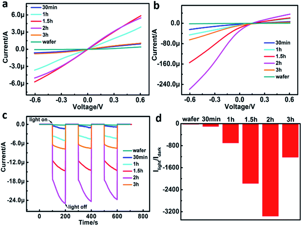 | ||
| Fig. 4 The I–V curve of p-SiNWs/ITO heterojunction under (a) dark and (b) visible LED conditions, (c) photocurrent under zero bias when illumination is turned on (100 s) and off (100 s), repeated for three cycles, (d) photosensitivity of heterojunctions with different length of SiNWs prepared by different etching time (wafer, 30 min, 1 h, 1.5 h, 2 h, 3 h). | ||
To determine the sensing characteristics of the self-powered sensor, the I–V characteristics of p-SiNWs/ITO heterojunction under N2 and 5 ppm NO2 atmosphere were measured respectively (Fig. 5a and b). The I–V curves showed different behavior when the device was alternatively exposed to N2 and NO2 under dark (black and blue) and illumination (red and purplish red) conditions. As shown in Fig. 5a, upon exposure to 5 ppm NO2, the photocurrent sharply drops at negative voltage than that at positive voltage under illumination. However, under the dark condition, the photocurrent response at negative voltage is almost the same as that at positive voltage (Fig. 5b). The result indicated that the photocurrent generated by the heterojunction between nanowire and ITO can sensitively respond to the gas dosing. The open-circuit current–time (I–t) curve of the device under light illumination (λ = 576 nm, P = 20 mW cm−2) was obtained at zero bias voltage (Fig. 5c). Before the dosing of NO2 gas, the device was equilibriumed in dry N2 gas under dark condition. Upon turning on light, the device produced an 8 μA negative photocurrent. After exposing with NO2, the sensor displayed positive photocurrent response, which increased with the increasing concentration of NO2 gas. The response (R) of the self-power NO2 sensor was defined according to the following equation:
| R = (I − I0)/I0 |
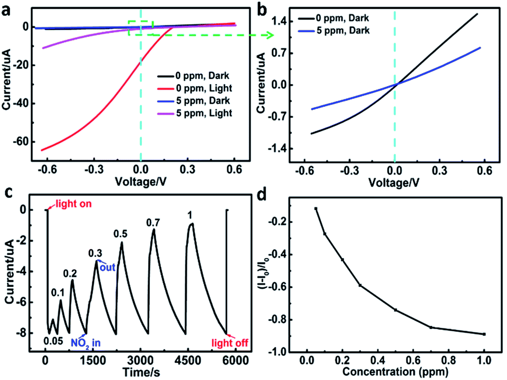 | ||
| Fig. 5 (a) Dark and light I–V curves of p-SiNWs/ITO heterojunction before (black, red) and after (blue, purplish red) 5 ppm NO2 importing respectively, (b) the amplification of the I–V curve in dark condition (c) real-time NO2 detection with different concentrations (ppm) of p-SiNWs/ITO heterojunction (d) the linear relationship between the relative response and concentration, the SINWs etching time was 2 h. | ||
Sensing mechanism
The high photosensitivity and gas sensitivity of the device are attributed to the photocatalysis of HF-treated SiNWs and the combined actions of the SiNWs and ITO. For the photosensitivity performance, except the excellent light reflection suppression effect of SiNWs, the HF-treated process was also very important. If the SiNWs weren't treated by the HF, the photocurrent can't be sustainable (Fig. S8†). This is because hydrogen atom has a large Pauling electron negative value of 2.2; consequently, the terminated hydrogen atom with a charge of 0.09–0.13 au may serve as an electron sink and accelerate the separation of the photoinduced electron and hole thus promote the photocatalytic efficiency.26 Beside above factors, the built-in electric field within the p-SiNWs array/ITO junction could also guarantee both a high photocurrent and a low dark current (10 nA at zero bias, Fig. 5c). For a pure p-type SiNWs gas sensors, the resistance would decrease when importing the oxidizing gases due to the increase of majority carriers. However, in this self-powered device, the photocurrent decreased in response to NO2, inferring that the mechanism of this structure cannot be explained just by the carrier change of SiNWs owing to the formation of p–n heterojunctions between p-SiNWs and ITO. Because of the different work function between p-SiNWs (∼1.12 eV)27 and ITO (∼3.5 eV),28 the carriers diffusion under thermal equilibrium conditions lead to the formation of a built-in electric field with a direction from ITO to p-SiNWs. The energy band diagram and its photovoltaic characteristics of the self-powered p-SiNWs/n-ITO are illustrated in Fig. 6. In the dark condition, the small forward bias could produce a positive current in the circuit. However, upon light illumination, the photoinduced electromotive force was in the reverse direction to the built-in bias, and therefore led to the current change from positive to negative. When illuminated by light, electron–hole pairs generate in the SiNWs and then inject the excited electrons (e−) from the conduction band of SiNWs into the conduction band of ITO, whilst the mismatch in the valence band and absence of a hole extracting agent forces holes to remain in SiNWs.29 Ongoing injection of electrons increases the number of holes within SiNWs leading to a transient electrical polarization corresponding to (dynamic) accumulations of holes (SiNWs) and electrons (ITO). This is a self-limiting process that continues until the formed electric field blocks any further injections of electrons, leading to generation of a photocurrent in the external circuit.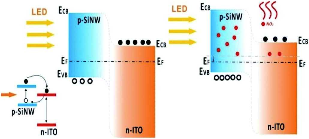 | ||
| Fig. 6 The sensing mechanism of p-SiNWs/ITO before and after importing NO2 under visible light illumination, respectively. | ||
Under NO2 atmosphere, the electrons accumulated at the SiNWs/ITO interface can be trapped by NO2 molecules, the trapped electrons at the junction are subsequently compensated by bulk ITO electrons, causing a decrease in the apparent donor density within the metal oxide (ND decreases). The equations of the semiconductor quantum theory can be used to support the above-described mechanism.29,30 The relation between the donor concentration (ND) and the built-in potential Vbi in a p–n junction is expressed by
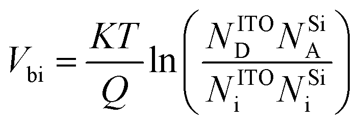 | (1) |
Conclusion
In summary, we have fabricated and investigated a photo-driving self-powered p-SiNW/ITO heterojunction device, in which the tip of the SiNWs was directly in contact with the ITO electrode and gas analytes could diffuse into the SiNW array. Under visible light illumination, the device showed high photosensitivity and ultrafast response speeds under zero bias voltage, and displayed a distinctive binary response under a small forward bias. The device can sensitively and quantitatively respond to NO2 gas without the need of external power. In comparison with chemiresistive sensors based on SiNWs only, the sensitivity of the self-powered sensor was improved. More importantly, the photodiode-structure nanosensor can persistently output electrical power by harvesting light energy, and in the meantime monitor the surrounding gas without a power supply. This work may have a huge application in the fields of environmental sensing, biosensing, and optoelectronic integrated circuits and bring about a novel idea and a facile method to develop self-powered gas microsensors based on the rational design of p–n heterojunctions using nanomaterials.Experimental
Materials
P-type silicon wafers (1 0 0 crystal, boron-doped, 5–10 Ω cm) and N-type Si (1 0 0) wafers (phosphor-doped, 1–10 Ω cm) were purchased from Beijing XiHe Ruida Technology Co. (China). ITO (<15 ohm sq−1) was purchased from Zhuhai Kaivo Optoelectronic Technology Co. (China). HF (40%), H2O2 (30%), AgNO3 (>99.9%), HNO3 (65–68%), ethanol (≥99.7%), acetic acid (≥99.5%) were purchased from Sinopharm Chemical Reagent Co. (China). The standard NO2 gas sample with concentration of 16.8 ppm (diluted in N2) was purchased from Hangzhou Xinshiji Mixed Gas Co. (China).Preparation of SiNWs array
Si wafers were cut into pieces with dimension of 5 × 5 mm2. The silicon nanowires (SiNWs) were prepared by metal assisted chemical etching (MACE) similar to the method as described previously.33 Briefly, the Si wafers were immersed in 0.008 M AgNO3 and 4.8 M HF for 2 min at room temperature. After the Ag nanoparticles formed, the wafers were washed with deionized water to remove the remained Ag+ ions, and then etched in 4.8 M HF and 0.4 M H2O2 for 2 h under room temperature. Then the wafers were washed repeatedly with deionized water and immersed in the HNO3 water solution (1![[thin space (1/6-em)]](https://www.rsc.org/images/entities/char_2009.gif) :1 v/v) for 30 min to dissolve the remained Ag particles. After that the as-prepared SiNWs were immersed in 3.3% HF solution for 10 min to remove the oxide layer. Finally, it was cleaned with deionized water and ethanol and dried under N2 flow.
:1 v/v) for 30 min to dissolve the remained Ag particles. After that the as-prepared SiNWs were immersed in 3.3% HF solution for 10 min to remove the oxide layer. Finally, it was cleaned with deionized water and ethanol and dried under N2 flow.
Characterization and gas detection system
The morphologies of the synthesized SiNWs arrays were investigated using field-emission scanning electron microscopy (FE-SEM, Hitachi SU 8010) with an operating voltage of 5 kV and magnification of 2500 were applied.The SiNWs/ITO structure is basically constructed by compressing the transparent ITO and the tip of SiNWs with proper pressure. In order to investigate the performance of gas sensing, the SiNWs/ITO sensor was sealed into a chamber with a window for light illumination and the volume of the chamber was ∼2 cm3. The concentration of NO2 gas sample was adjusted by mixing the standard NO2 sample (16.8 ppm) with N2 at a specific ratio controlled by an automatic gas mixing apparatus (National Institute of Metrology, China). The total flow rate of the mixture was kept at 200 ml min−1. The light illumination comes from a LED (S2000, Nanjing Hecho Technology Co., China) emitting white light. The light intensity in the chamber was 20 mW cm−2, which was measured by an optical power meter (SGN-1, Shanghai Shuoguang Optoelectronic Technology Co., China). The sealed chamber was kept at room temperature. The current–voltage (I–V) data of SiNW/ITO heterojunction were recorded by a Keithley 6487 digital source-meter.
Conflicts of interest
There are no conflicts to declare.Acknowledgements
This work was supported by National Science Foundation of China (No. 21575127), and Zhejiang Provincial Natural Science Foundation of China (No. Z15B050001).Notes and references
- J. A. Rogers and Y. Huang, Proc. Natl. Acad. Sci. U. S. A., 2009, 106, 10875–10876 CrossRef CAS PubMed.
- L. Yuan, J. Dai, X. Fan, T. Song, Y. T. Tao, K. Wang, Z. Xu, J. Zhang, X. Bai and P. Lu, ACS Nano, 2011, 5, 4007 CrossRef CAS PubMed.
- L. Yuan, Y. Tao, J. Chen, J. Dai, T. Song, M. Ruan, Z. Ma, G. Li, L. Kang and X. Zhang, Adv. Funct. Mater., 2011, 21, 2150–2154 CrossRef CAS.
- Z. L. Wang, Adv. Mater., 2012, 24, 280–285 CrossRef CAS PubMed.
- Z. L. Wang, Adv. Funct. Mater., 2008, 18, 3553–3567 CrossRef CAS.
- X. Xu, T. Ding, L. Yuan, Y. Shen, Q. Zhong, X. Zhang, Y. Cao, B. Hu, Z. Teng and G. Li, Adv. Energy Mater., 2012, 2, 1328–1332 CrossRef.
- Z. L. Wang, Nano Today, 2010, 5, 512–514 CrossRef.
- X. Xiao, L. Yuan, J. Zhong, T. Ding, Y. Liu, Z. Cai, Y. Rong, H. Han, J. Zhou and Z. L. Wang, Adv. Mater., 2011, 23, 5440–5444 CrossRef CAS PubMed.
- Z. L. Wang, Sci. Am., 2008, 298, 82–87 CrossRef PubMed.
- X. Xue, Y. Nie, B. He, L. Xing, Y. Zhang and Z. L. Wang, Nanotechnology, 2013, 24, 225501 CrossRef PubMed.
- R. Zhang, L. Lin, Q. Jing, W. Wu, Y. Zhang, Z. Jiao, L. Yan, R. P. Han and Z. L. Wang, Energy Environ. Sci., 2012, 5, 8528–8533 RSC.
- Y. Hu, C. Xu, Y. Zhang, L. Lin, R. L. Snyder and Z. L. Wang, Adv. Mater., 2011, 23, 4068–4071 CrossRef CAS PubMed.
- N. Cui, W. Wu, Y. Zhao, S. Bai, L. Meng, Y. Qin and Z. L. Wang, Nano Lett., 2012, 12, 3701–3705 CrossRef CAS PubMed.
- A. Gad, M. W. Hoffmann, O. Casals, L. Mayrhofer, C. Fàbrega, L. Caccamo, F. Hernández-Ramírez, M. S. Mohajerani, M. Moseler and H. Shen, ACS Sens., 2016, 1, 1256–1264 CrossRef CAS.
- N. M. Vuong, N. M. Hieu, H. N. Hieu, H. Yi, D. Kim, Y.-S. Han and M. Kim, Sens. Actuators, B, 2014, 192, 327–333 CrossRef.
- K. Peng, X. Wang and S.-T. Lee, Appl. Phys. Lett., 2008, 92, 163103 CrossRef.
- Y. Cao, J.-H. He, J.-L. Zhu and J.-L. Sun, Chem. Phys. Lett., 2011, 501, 461–465 CrossRef CAS.
- Y. Cui, X. Duan, J. Hu and C. M. Lieber, J. Phys. Chem. B, 2000, 104, 5213–5216 CrossRef CAS.
- M. Zhu, X. Li, S. Chung, L. Zhao, X. Li, X. Zang, K. Wang, J. Wei, M. Zhong and K. Zhou, Carbon, 2015, 84, 138–145 CrossRef CAS.
- G. Li, L. Liu, G. Wu, W. Chen, S. Qin, Y. Wang and T. Zhang, Small, 2016, 12, 5019–5026 CrossRef CAS PubMed.
- M. W. Hoffmann, L. Mayrhofer, O. Casals, L. Caccamo, F. Hernandez-Ramirez, G. Lilienkamp, W. Daum, M. Moseler, A. Waag and H. Shen, Adv. Mater., 2014, 26, 8017–8022 CrossRef CAS PubMed.
- M. W. Hoffmann, A. E. Gad, J. D. Prades, F. Hernandez-Ramirez, R. Fiz, H. Shen and S. Mathur, Nano Energy, 2013, 2, 514–522 CrossRef CAS.
- Y. Jia, Z. Zhang, L. Xiao and R. Lv, Nanoscale Res. Lett., 2016, 11, 299 CrossRef PubMed.
- H. Fang, X. Li, S. Song, Y. Xu and J. Zhu, Nanotechnology, 2008, 19, 255703 CrossRef PubMed.
- G. Yuan, H. Zhao, X. Liu, Z. S. Hasanali, Y. Zou, A. Levine and D. Wang, Angew. Chem., Int. Ed., 2009, 48, 9680–9684 CrossRef CAS PubMed.
- M. Shao, L. Cheng, X. Zhang, D. D. D. Ma and S.-t. Lee, J. Am. Chem. Soc., 2009, 131, 17738–17739 CrossRef CAS PubMed.
- Y. Cui, Z. Zhong, D. Wang, W. U. Wang and C. M. Lieber, Nano Lett., 2003, 3, 149–152 CrossRef CAS.
- H. Kim, a. C. Gilmore, A. Pique, J. Horwitz, H. Mattoussi, H. Murata, Z. Kafafi and D. Chrisey, J. Appl. Phys., 1999, 86, 6451–6461 CrossRef CAS.
- J. Piris, A. J. Ferguson, J. L. Blackburn, A. G. Norman, G. Rumbles, D. C. Selmarten and N. Kopidakis, J. Phys. Chem. C, 2008, 112, 7742–7749 CrossRef CAS.
- S. Sze, Physics of semiconductor devices, 2007, vol. 3 Search PubMed.
- B. Kaplan, Phys. B, 2004, 351, 90–95 CrossRef CAS.
- X. Chao, Y. Ruo-He and G. Kui-Wei, Chin. Phys. B, 2011, 20, 057302 CrossRef.
- D. Liu, L. Lin, Q. Chen, H. Zhou and J. Wu, ACS Sens., 2017, 2, 1491–1497 CrossRef CAS PubMed.
Footnote |
| † Electronic supplementary information (ESI) available. See DOI: 10.1039/c9ra02972a |
| This journal is © The Royal Society of Chemistry 2019 |