
 Open Access Article
 This Open Access Article is licensed under a Creative Commons Attribution-Non Commercial 3.0 Unported Licence
Charge transport and extraction of PTB7:PC71BM organic solar cells: effect of film thickness and thermal-annealing
Yingying Zhang,
Xiong Li *,
Tingting Dai,
Denghui Xu,
Jianfeng Xi and
Xiaobai Chen
*,
Tingting Dai,
Denghui Xu,
Jianfeng Xi and
Xiaobai Chen
Department of Physics, Beijing Technology and Business University, Beijing 100048, P. R. China. E-mail: lixiong@btbu.edu.cn; Tel: +86 10 81353607
First published on 12th August 2019
Abstract
Charge carrier transport in the active layer and charge extraction at the electrode have significant impact on the performance of solar cells. In this study, the effect of active layer thickness and thermal-annealing treatment on the charge transport and extraction performance of PTB7:PC71BM organic solar cells was studied comprehensively. Thin films of active layer couldn't utilize enough sunlight, while thick films could bring about large bulk resistance and deteriorate carrier transport. There is a trade-off between active layer thickness and carrier transport. The optimized active layer thickness is about 100 nm for the PTB7:PC71BM bulk heterojunction organic solar cells. Thermal-annealing could improve the morphology of the active layer, and facilitate charge transport in the active layer and charge collection at the electrode. The improved carrier transport and extraction were verified by the transient photocurrent/transient photovoltage and photo-induced charge carrier extraction by linearly increasing voltage measurements. The optimal power conversion efficiency was obtained as 8.28% for the device with an active layer thickness of 100 nm and treated with 90 °C thermal-annealing.
1. Introduction
Organic solar cells (OSCs) have been widely studied for their unique advantages of low production cost, mechanical flexibility and environmental friendliness, which make them a potential candidate for next generation green energy sources.1–3 Recently, continuous breakthroughs in the power conversion efficiency (PCE) of OSCs4–6 have attracted much attention both in industry and academia. In the study of OSCs, bulk heterojunction (BHJ) is the most commonly used device structure, which blends donor and acceptor materials together in nanoscale and provides a bi-continuous interpenetrating network for efficient exciton dissociation and charge transport.7 Almost all the remarkable PCE improvement has been achieved by using the BHJ structure for the past few years.8–10 The efficiency of OSCs is determined by the light absorption of active layer, exciton generation and dissociation efficiency, charge transport efficiency and charge collection efficiency. For utilizing more incident light, thick active layer film is needed, however the low carrier mobility of organic semiconductors11,12 limit the thickness of active layer. There is an optimized thickness of active layer for the high-efficiency OSCs. Besides enhancing light absorption, various methods have also been incorporated in the manufacturing process to improve charge transport and extraction, including thermal-annealing,13,14 solvent vapor annealing,15,16 solvent additive,17,18 interface engineering,19,20 and so on. Among these processing methods, thermal-annealing treatment the active layer films at appropriate temperature can modify the nanoscale phase separation and improve the crystallization of OSCs blends within the BHJ networks, facilitate charge transport to the electrodes and increase the PCE.21,22 Thermal-annealing is a low-cost, convenient and effective strategy to improve the film morphology and boost performance of BHJ based OSCs.23The low band gap polymeric donor material poly[[4,8-bis[(2-ethylhexyl)oxy]benzo[1,2-b:4,5-b′]dithiophene-2,6-diyl][3-fluoro-2-[(2-ethylhexyl)carbonyl]thieno[3,4-b]thiophenediyl]] (PTB7) has attracted great interest in recent years due to its high performance in BHJ solar cells based on PTB7:[6,6]-phenyl-C71-butyric acid methyl ester (PC71BM) active layer system.24–26 However, most of the studies about PTB7:PC71BM solar cells have focused on the performance improvement by using solvent additive,27,28 mixed solvent,29,30 interface modification31,32 and so on. There have been few reports about the effect of active layer thickness and thermal-annealing on the performance of PTB7:PC71BM BHJ organic solar cells.
In this study, we prepared BHJ organic solar cells with PTB7:PC71BM as active layer, and studied detailedly the effect of active layer thickness and thermal-annealing treatment on the charge transport and extraction performance of PTB7:PC71BM organic solar cells. The results show that the thickness of active layer affects charge transport in the active layer obviously, and there is a trade-off between light absorption and carrier transport. The optimized PCE was achieved for the device with active layer thickness of 100 nm. Thermal-annealing could improve the morphology of active layer, and further promote exciton dissociation efficiency, improve charge transport and extraction efficiency of the OSCs. The optimal PCE was obtained as 8.28% for the device with active layer thickness of 100 nm and 90 °C thermal-annealing. The results suggest that active layer thickness optimization and thermal-annealing treatment are simple and effective methods to improve the performance of PTB7:PC71BM organic solar cells. This study is expected to be helpful to understand deeply the charge transport and extraction of the bulk heterojunction and provide a useful guideline for optimizing device performance of OSCs.
2. Experiment
2.1 Material
PTB7 was used as electron donor material and PC71BM was used as acceptor material, and both of them were purchased from 1-Material Inc. Poly-(3,4-ethylene-dioxythiophene):poly(styrene sulfonate) (PEDOT:PSS) (Clevios P Al4083, Heraeus Precious Metals GmbH & Co. KG) was used as hole-conducting material and passed through a 0.45 μm filter before spin-coating. Chlorobenzene (CB) and 1, 8-diiodoctane (DIO) was purchased from Sigma-Aldrich. All reagents were used as received without further treatment.2.2 Devices fabrication
The device structure of OSCs was indium tin oxide (ITO)/PEDOT:PSS (∼40 nm)/PTB7:PC71BM (with DIO)/Ca (∼20 nm)/Al (∼60 nm). The active layer solution was prepared by dissolving PTB7 and PC71BM with a weight ratio of 1![[thin space (1/6-em)]](https://www.rsc.org/images/entities/char_2009.gif) :1.5 (10 mg ml−1 PTB7, 15 mg ml−1 PC71BM) with 3% v/v of DIO solvent as additive to form the mixed solution and then stir at 70 °C in the dark for 24 h.
:1.5 (10 mg ml−1 PTB7, 15 mg ml−1 PC71BM) with 3% v/v of DIO solvent as additive to form the mixed solution and then stir at 70 °C in the dark for 24 h.
For the device fabrication, the ITO glass substrates (with sheet resistance of 15 Ω Sq−1) were cleaned with detergent, followed by sequential sonication in deionized water, acetone, ethanol each for 20 min, and then dried by high pure nitrogen gas. Subsequently, the pre-cleaned ITO substrates were exposed to ultraviolet–ozone for 8 min for further cleaning and improving work function of ITO. PEDOT:PSS was spin-coated on the pre-cleaned ITO coated glass-substrate with a thickness of 40 nm and then thermal annealed at 140 °C for 30 min. Next, all the substrates were transferred into nitrogen-filled glove box (<0.01 ppm O2 and H2O) for further processing. The active layer was then fabricated by spin coating the PTB7:PC71BM blend solution on the top of PEDOT:PSS layer, and the thickness of active layer was controlled by spin-coating rates (shown in Table 1). The active layer films with thickness of 100 nm were thermal-annealed for 10 min at different temperature. Finally, about 20 nm Ca and 60 nm Al were thermally deposited on the active layer under the vacuum of 2 × 10⁻⁴ Pa. The deposition rate and thickness of Ca and Al were recorded by quartz-crystal oscillator monitors. The device area is 4.5 mm2 which was defined by the vertical overlap of ITO anode and Al cathode.
| Rotation speed (rpm) | Thickness (nm) | Jsc (mA cm−2) | Voc (V) | FF | PCE (%) |
|---|---|---|---|---|---|
| 2100 | 70 | 14.19 ± 0.28 | 0.68 ± 0.01 | 0.61 ± 0.01 | 5.89 ± 0.06 |
| 1800 | 90 | 16.33 ± 0.29 | 0.69 ± 0.01 | 0.62 ± 0.01 | 6.99 ± 0.08 |
| 1500 | 100 | 16.39 ± 0.24 | 0.70 ± 0.01 | 0.63 ± 0.01 | 7.23 ± 0.08 |
| 1200 | 120 | 15.98 ± 0.25 | 0.69 ± 0.01 | 0.61 ± 0.01 | 6.73 ± 0.05 |
| 900 | 130 | 14.95 ± 0.22 | 0.67 ± 0.01 | 0.62 ± 0.01 | 6.21 ± 0.04 |
| 1500 | 100 | 17.31 ± 0.27 | 0.70 ± 0.01 | 0.62 ± 0.01 | 7.51 ± 0.06 |
| 1500 | 100 | 18.10 ± 0.21 | 0.75 ± 0.01 | 0.61 ± 0.01 | 8.28 ± 0.10 |
| 1500 | 100 | 16.31 ± 0.20 | 0.75 ± 0.01 | 0.58 ± 0.01 | 7.09 ± 0.09 |
| 1500 | 100 | 15.89 ± 0.28 | 0.73 ± 0.01 | 0.56 ± 0.01 | 6.47 ± 0.06 |
2.3 Devices characterization
The thicknesses of the PEDOT:PSS layer, active layer, Ca and Al layer were measured by Bruker Stylus Profile (DektakXT, Bruker Corporation, American). The current density–voltage (J–V) characteristics of the OSCs were recorded by using a Keithley2400 source meter unit under 100 mW cm−2 illumination with AM 1.5 solar simulator (San-Ei Electric). The ultraviolet-visible (UV-Vis) absorption spectra on quartz substrates were determined by a Hatachi-U3900H spectrophotometer. The external quantum efficiency (EQE) was measured with a solar cell QE/IPCE measurement system (Zolix solar cell scan100). The morphologies of the active layer films were investigated by ez-AFM Atomic Force Microscope (NanoMagnetics Instruments, England). Photo-induced charge carrier extraction by linearly increasing voltage (Photo-CELIV), transient photocurrent (TPC) and transient photo-voltage (TPV) measurements were performed using the commercially available Paios system (FLUXiM AG, Switzerland). A high-power white LED is implemented as light source of transient and Photo-CELIV measurements. The integrated power of the LED is 720 W m−2. The spectrum distribution is mainly in the wavelength range of 440–470 nm and 540–630 nm, and the peak value is about 460 nm and 550 nm.3. Results and discussion
In order to evaluate the effect of film thickness and thermal-annealing on the morphology of active layer, we studied the surface topography and phase images of the active layer films with AFM. Fig. 1 shows the AFM images of PTB7:PC71BM active layer films with different thickness. The bright clusters appearing in dark region are considered as PC71BM rich domains embedded in the polymer matrix.22,33 It can be seen that PC71BM is relatively evenly distributed in this films. The surface roughness varies with changing active layer thickness. The Root-Mean-Square (RMS) decreases with increasing the thickness of the active layer from 70 nm to 100 nm, and then increases with further changing the thickness of the active layer from 100 nm to 130 nm. When the thickness of the active layer film is 100 nm, the film exhibits the minimum roughness with the RMS value of 1.38 nm, and the phase image of Fig. 1h indicates that the film has good phase separation. The good phase separation is in favor of carrier transport in the active layer and thus improves photocurrent.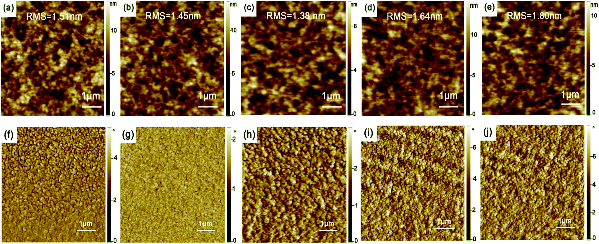 | ||
| Fig. 1 The AFM surface topography of the PTB7:PC71BM films with different active layer thickness (a) 70 nm; (b) 90 nm; (c) 100 nm; (d) 120 nm; (e) 130 nm; (f–j) the corresponding phase diagram at the bottom. | ||
Fig. 2 reveals the active layer morphology with different thermal-annealing temperature. For the active layer without thermal-annealing, the RMS is 1.38 nm, when the active layer films was annealed at low temperature (70 °C and 90 °C) for 10 min, the RMS decreases slightly. With further raising annealing temperature, the RMS increases obviously, and the active layer treated with 110 °C and 140 °C show the RMS values of 1.84 nm and 2.56 nm, respectively. With high temperature thermal-annealing, polymer crystallization size becomes large in the active layer, thereby increasing the overall surface roughness of the films.
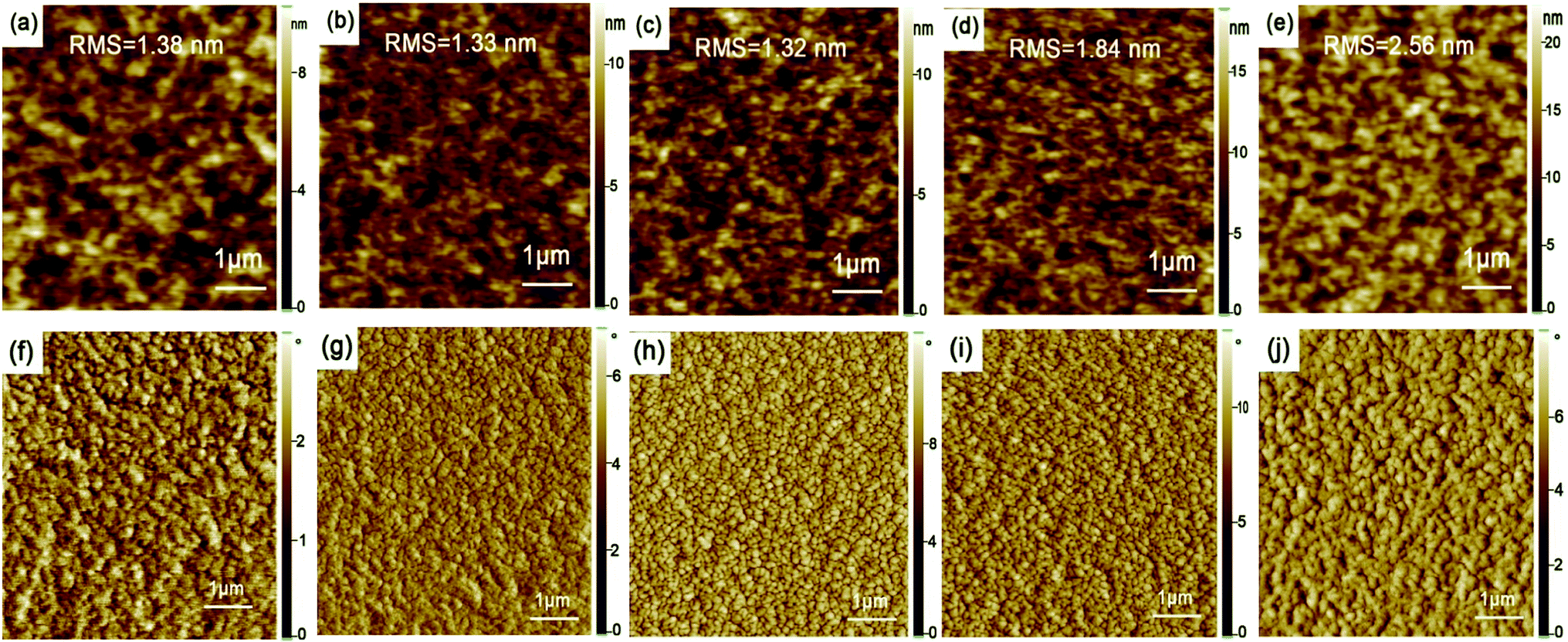 | ||
| Fig. 2 The AFM surface topography of the PTB7:PC71BM films treated with different thermal-annealing temperature (a) without annealing; (b) thermal-annealing at 70 °C; (c) at 90 °C; (d) at 110 °C; (e) at 140 °C; (f–j) the corresponding phase diagram. The thickness of all the thermal-annealed films is 100 nm. | ||
Fig. 3a illustrates the UV-Vis absorption spectra of the PTB7:PC71BM active layer films with different thickness. The absorption in the short wavelength range of 350–500 nm correspond to PC71BM, while the absorption range from 600 nm to 750 nm was mainly attributed to PTB7.34,35 The absorption spectrum clearly manifests that the thicker active layer films bring about stronger absorption. The active layer with thickness of 130 nm shows the best light absorption, while the absorption ability of the film with thickness of 70 nm is weaker. The UV-Vis absorption spectra of the PTB7:PC71BM active layer films (with thickness of 100 nm) treated with thermal-annealing at different temperatures are shown in Fig. 3b. Compared with the active layer without thermal-annealing treatment, the absorption peak of annealed films did not shift, only the intensity of absorption peak changed. In the whole wavelength range, the absorption intensity of the active layer with 90 °C thermal-annealing is a slightly higher than that of others. The peak intensity is determined by the structural order of the PTB7 and PC71BM in the active layer film.33,36 The increased peak intensity of the active layer under thermal-annealing at 70 °C and 90 °C should attributed to the orderly stacking of the polymer chain upon gradual increase in annealing temperature, as previously reported.33,36 While the decreased peak intensity of the films with 110 and 140 °C thermal-annealing implies that high temperature deteriorate the structural order. The improved structural order of polymer PTB7 is beneficial to charge transport in the active layer.
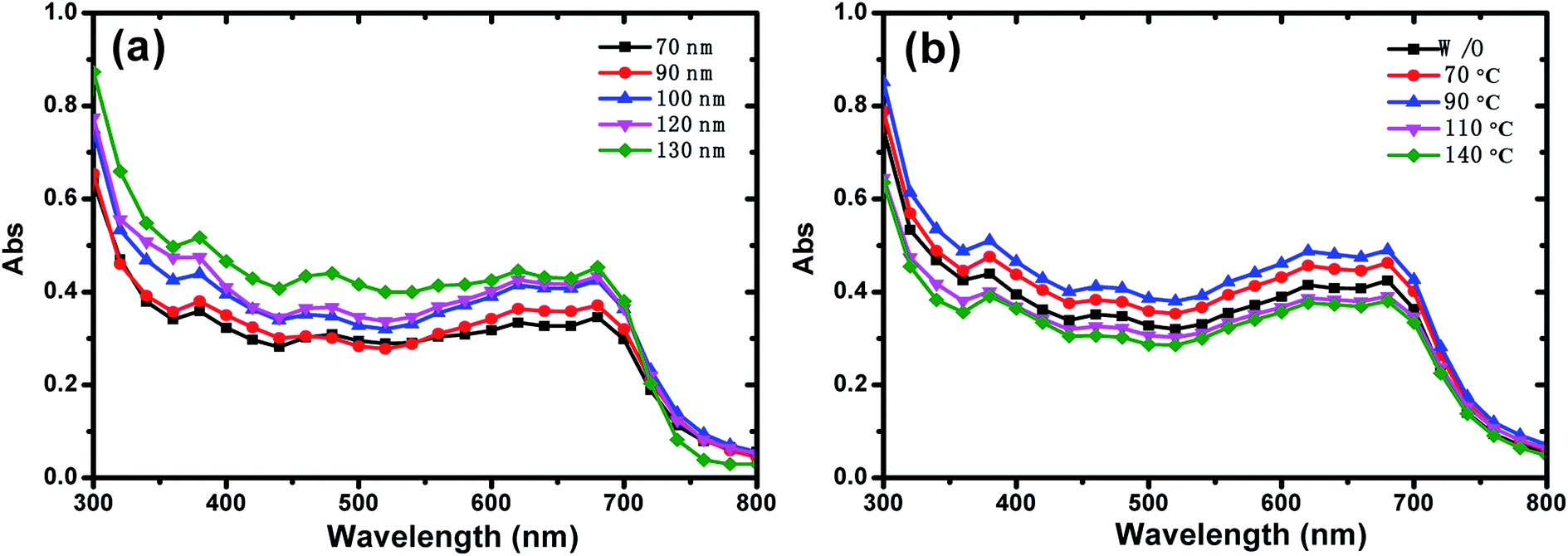 | ||
| Fig. 3 UV-Vis absorption spectra of the active layer films (a) with different films thickness and (b) with different thermal-annealing temperature based on the active layer thickness of 100 nm. | ||
Fig. 4a shows the J–V characteristics of organic solar cells with different active layer thicknesses, which were measured under AM 1.5 illumination at 100 mW cm−2. The corresponding photovoltaic parameters including short circuit current density (Jsc), open circuit voltage (VOC), fill factor (FF), PCE, extracted from the J–V curves, were summarized in Table 1. The values of photovoltaic parameters were obtained from at least 8 identical devices for each case. With increasing active layer thicknesses from 70 nm to 100 nm, the Jsc raises from 14.19 to 16.39 mA cm−2. However, the Jsc begins to fall with further increasing active layer thickness. When the active layer thickness reaches 130 nm, the Jsc reduces to 14.95 mA cm−2. As can be seen from Table 1, the VOC and FF have slight changes. The main reason for the PCE improvement is Jsc, and the optimized PCE was achieved in the device with active layer thickness of 100 nm. Light absorption is an important factor that affects Jsc. Thicker active layer films could absorb more sunlight; however, thicker active layer could also bring about larger bulk resistance that would hinder carriers transport in the active layer and deteriorate the performance of OSCs.29 Therefore, the 130 nm active layer displays the highest absorption characteristic while the corresponding device presents the lowest EQE performance. The inferior carrier mobility of organic materials limits the thickness of active layer, thus there is a trade-off between active layer thickness and carrier mobility. Based on the overall photovoltaic performance in Table 1, 100 nm is the rational thickness of active layer in this study.
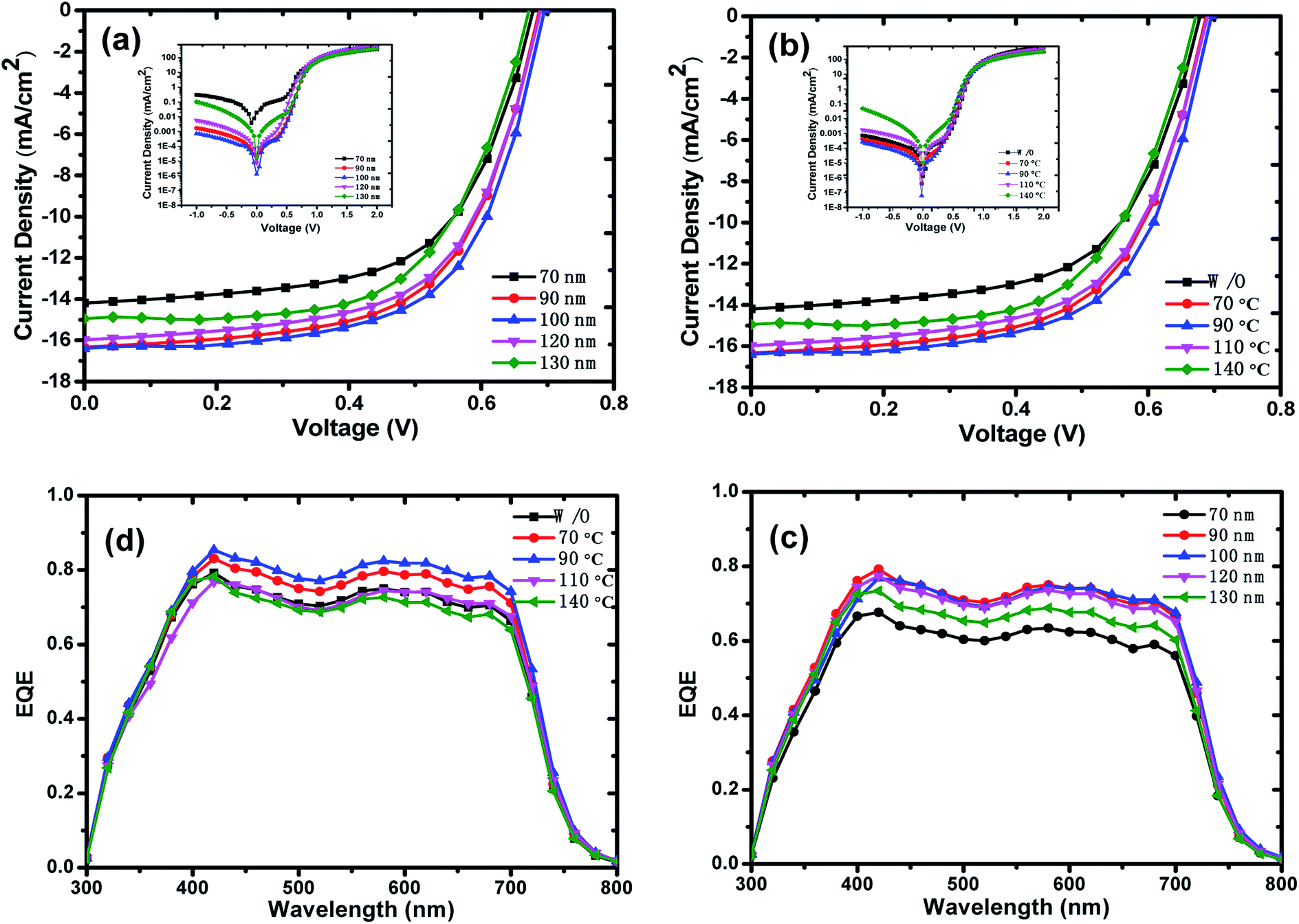 | ||
| Fig. 4 The J–V characteristic curves of the OSCs (a) with different film thickness and (b) with different thermal-annealing temperature under simulated solar AM 1.5 illuminations at 100 mW cm−2 (the inset is J–V characteristic curves under dark); the EQE spectra of the OSCs (c) with different films thickness and (d) different thermal-annealing temperature. | ||
The dark J–V characteristics were measured to further study the effect of film thickness on the shunt resistance and series resistance, and thus the FF of devices. Large shunt resistance and small series resistance is beneficial to obtaining higher FF. At reverse bias region of the dark J–V curves, the current is mainly limited by the shunt resistance due to leakage current.37,38 As the active layer thickness increases, the leakage current decreases first and then increases at the reverse bias region of the dark J–V curves as shown in the inset of Fig. 4a. Compared with 100 nm thick device, the device with 70 nm active layer thickness exhibits a larger leakage current, which would decrease the shunt resistance, and then reduce FF. The larger leakage current is suggested to be originated from the additional current pathways formed by the defects of active layer/Al electrode interface, which is evidenced by the roughness of the AFM diagram shown in Fig. 1. At high positive voltages region of the dark J–V curves, the dark current is mainly controlled by series resistance.37,39 The higher dark current of the 100 nm thickness device indicates that the appropriate phase separation (Fig. 1h) of active layer film and smooth active layer/Al interface facilitate charge transport and extraction, which decrease the series resistance and improve the FF.
For studying the influence of thermal-annealing on the performance of PTB7:PC71BM organic solar cells, we prepared the devices with active layer thickness of 100 nm and thermal-annealed them at 70, 90, 110 and 140 °C, respectively. The J–V characteristics of the devices with different thermal-annealing temperature were shown in Fig. 4b, and the corresponding photovoltaic parameters were summarized in Table 1. For the devices with thermal-annealing, the value of Jsc increases with increasing the thermal-annealing temperature from 70 °C to 90 °C, and then decreases for further enhancing thermal-annealing temperature, and the maximum value of Jsc is gained as 18.10 mA cm−2 for the device with 90 °C thermal-annealing. As compared with the devices without thermal-annealing, the VOC increases from 0.70 V to 0.75 V for the devices with thermal-annealed at 90 °C and 110 °C. Different from Jsc and VOC, the FF decreases obviously with increasing thermal-annealing temperature. As PCE was determined by Jsc, VOC and FF, the optimal PCE was obtained as 8.28% for the device with 90 °C thermal-annealing. Thermal-annealing at the proper temperature could improve structural order of polymer PTB7 in the active layer and optimize surface morphology of active layer, which would facilitate carrier transport and collection, and improve performance of OSCs. The dark J–V curves is shown in the inset of Fig. 4b. The single logarithmic dark current curve shows that the devices with 70 °C and 90 °C thermal-annealing have smaller leakage current than that of the device without thermal-annealing. The low leakage current density of 90 °C thermal-annealing device indicates that the annealing at proper temperature can inhibit the charge carriers recombination and improve Jsc, so as to realize good efficiency of photoelectric conversion.
The EQE measurements were conducted to further investigate the contribution of incident photons to the photocurrent, and Fig. 4c and d display the EQE spectrum measured in the wavelength range from 300 nm to 800 nm. The EQE values exhibit an upward trend for the devices with active layer thickness increasing from 70 nm to 100 nm. Nevertheless, when further increasing the thickness of the active layers, the EQE values of these devices show downward trend. The EQE result is in accordance with the Jsc shown in Fig. 4a. As can been seen in Fig. 4d, for the devices with active layer thickness of 100 nm, thermal-annealing treatment affects the EQE values obviously. 70 °C and 90 °C thermal-annealing increase the EQE dramatically, while 110 °C and 140 °C thermal-annealing decrease the EQE. The device with 90 °C thermal-annealing shows the highest EQE improvement from 400 nm to 700 nm, resulting in the best Jsc of 18.10 mA cm−2, which is consistent with the J–V characteristics.
The charge recombination dynamics and charge extraction process of the devices were studied via TPV and TPC measurements, respectively. The voltage decay under open circuit condition is attributed to the recombination of free charges, and the fast voltage decay indicates rapid recombination.40,41 Normalized TPV decay curves of the devices with different active layer thickness were presented in Fig. 5a. By the TPV experiment, the charge carrier lifetime at given bias illumination can be estimated directly from the exponential voltage decay. The equation for the lifetime in TPV analysis is a mono-exponential:  where A is a constant that fits to the peak height, t is time and τ is the decay time constant.41,42 The charge carrier recombination lifetimes extracted from the TPV decay curves are 4.11, 11.74, 17.78, 6.10 and 4.21 μs for devices with active layer thickness of 70, 90, 100, 120 and 130 nm, respectively. The longest carrier recombination lifetime of the device with active layer thickness of 100 nm indicates a reduced bimolecular recombination process, and the less recombination is in favor of Jsc improvement.
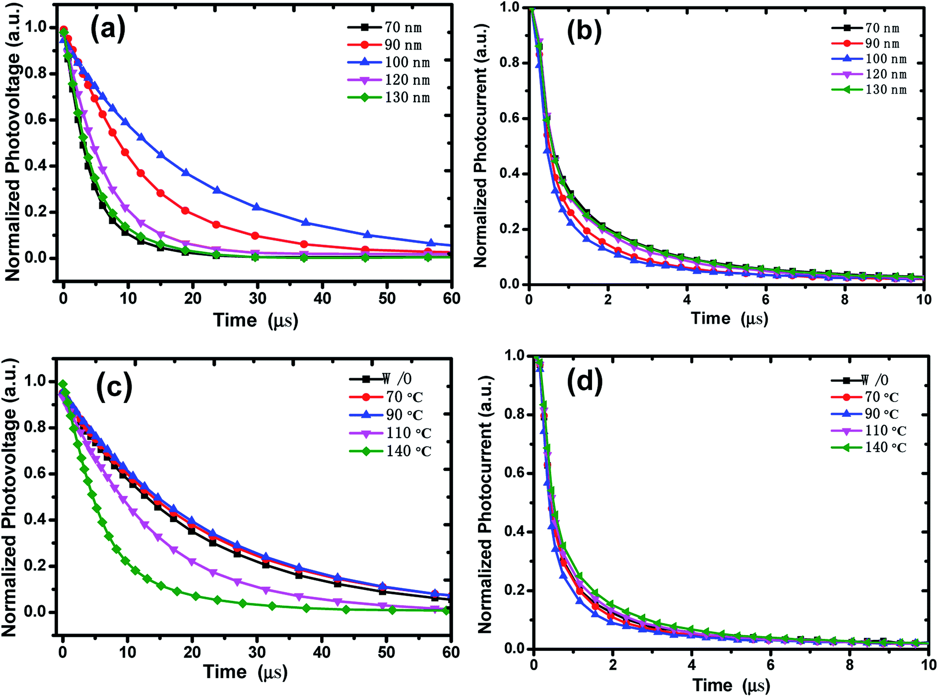 | ||
| Fig. 5 Normalized (a) TPV, (b) TPC decay curves with different films thickness; and the normalized (c) TPV, (d) TPC decay curves with different thermal-annealing temperature. | ||
In TPC experiments the current response to a light step is measured at constant offset-voltage.43,44 Charge extract time can be obtained from the TPC decay curves (Fig. 5b) which were measured under short circuit condition, and the charge extract time of each device was extracted from the normalized TPC decay curves by exponential fitting. The shorter charge extraction time means a faster carrier extraction rate. The charge extraction time of the devices with thickness of 70 nm is 0.475 μs. When the active layer thickness increases to 100 nm, the device shows the shortest charge extract time of 0.384 μs. For the device with 130 nm active layer, the charge extract time increases to 0.453 μs. The shortest charge extract time of the device with 100 nm thickness of active layer implies that the good morphology and relatively smooth active layer/Al interface improve charge transport in the active layer and charge collection at the electrode.
Fig. 5c and d show the normalized TPV/TPC decay curves of OSCs with different annealing temperature under active layer thickness of 100 nm. The charge carrier recombination lifetimes increase from 19.86 μs to 22.69 μs for the devices with 70 °C and 90 °C thermal-annealing, and then decrease for the devices with higher temperature annealing (110 °C and 140 °C), the recombination lifetime reduces to 6.28 μs for the 140 °C annealed device. The charge extract time are 0.372, 0.349, 0.406 and 0.424 μs for the devices with thermal-annealing temperature at 70, 90, 110 and 140 °C, respectively. The 90 °C thermal-annealed device shows the longest recombination lifetime and the shortest carrier extract time, which suggests that suitable annealing temperature could suppress charge recombination, facilitate carrier transport and collection, thus improve the performance of the devices.
The charge transport characteristics were further verified by the carrier mobility measurement with Photo-CELIV technique,44 and the corresponding photocurrent curves are shown in Fig. 6. In photo-CELIV measurement, free charge carriers are generated by a light pulse and are subsequently extracted by a voltage ramp.44,45 When the charge carriers are extracted from the bulk heterojunction, a current overshoot Δj = jmax − j0 is occurred. The time where the current peaks (tmax) can be used to calculate the charge carrier mobility by 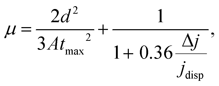 where μ is the charge carrier mobility, d is the active layer thickness, A is the ramp rate, tmax is the time where the current peaks, jdisp is the displacement current and Δj is the peak current minus the displacement current.45 The factor 1 + 0.36 Δj/jdisp in the formula is an empirical correction accounting for the redistribution of the electric field. The calculated mean mobilities are 3.50 × 10⁻⁵ cm2 V−1 s−1, 4.89 × 10⁻⁵ cm2 V−1 s−1, 5.68 × 10⁻⁵ cm2 V−1 s−1, 4.69 × 10⁻⁵ cm2 V−1 s−1 and 4.10 × 10⁻⁵ cm2 V−1 s−1 for the devices with active layer thickness of 70, 90, 100, 120 and 130 nm, respectively. The result is in accordance with TPV/TPC characteristic of Fig. 5. For 100 nm thickness devices with 70, 90, 110 and 140 °C thermal-annealing, the mobility are 5.94 × 10⁻⁵ cm2 V−1 s−1, 6.10 × 10⁻⁵ cm2 V−1 s−1, 5.48 × 10⁻⁵ cm2 V−1 s−1 and 4.70 × 10⁻⁵ cm2 V−1 s−1, respectively. The better carrier mobility is consistent with the performance of the devices with active layer thickness of 100 nm under 90 °C thermal-annealing, which indicates that the improved carrier transport between the two electrodes is one of the reasons for better performance of OSCs.
 | ||
| Fig. 6 Photo-CELIV curves of the devices (a) with different film thickness and (b) with different thermal-annealing temperature. | ||
To gain more insight into exciton dissociation and charge transfer characteristic of the OSCs, we studied the double-logarithmic plots of the net photocurrent Jph (Jph = Jlight − Jdark, where Jlight and Jdark are the current densities under illumination and dark conditions, respectively) against the effective voltage Veff (Veff = V0 − Va, where V0 is the voltage when Jph = 0 and Va is the applied bias voltage)36,46 as shown in Fig. 7. At large reverse voltage (Veff > 1.0 V), Jph is saturated and can be described approximately as Jsat = eGmax(E, T)L, where e is the elementary charge, L is the film thickness and Gmax(E, T) is the maximum exciton generation rate. It is believed that all the photo-generated excitons are dissociated into free charge carriers and collected by the electrodes at the saturation region. For the devices without thermal-annealing (Fig. 7a), the higher Jsat of the device with active layer of 100 nm indicates that more electron–hole pairs are generated at the PTB7/PC71BM interface, and then transferred to the electrode, which implies that active layer with rational thickness can not only utilize sunlight sufficiently, but also provide suitable carrier transport channels for electron and hole migration.
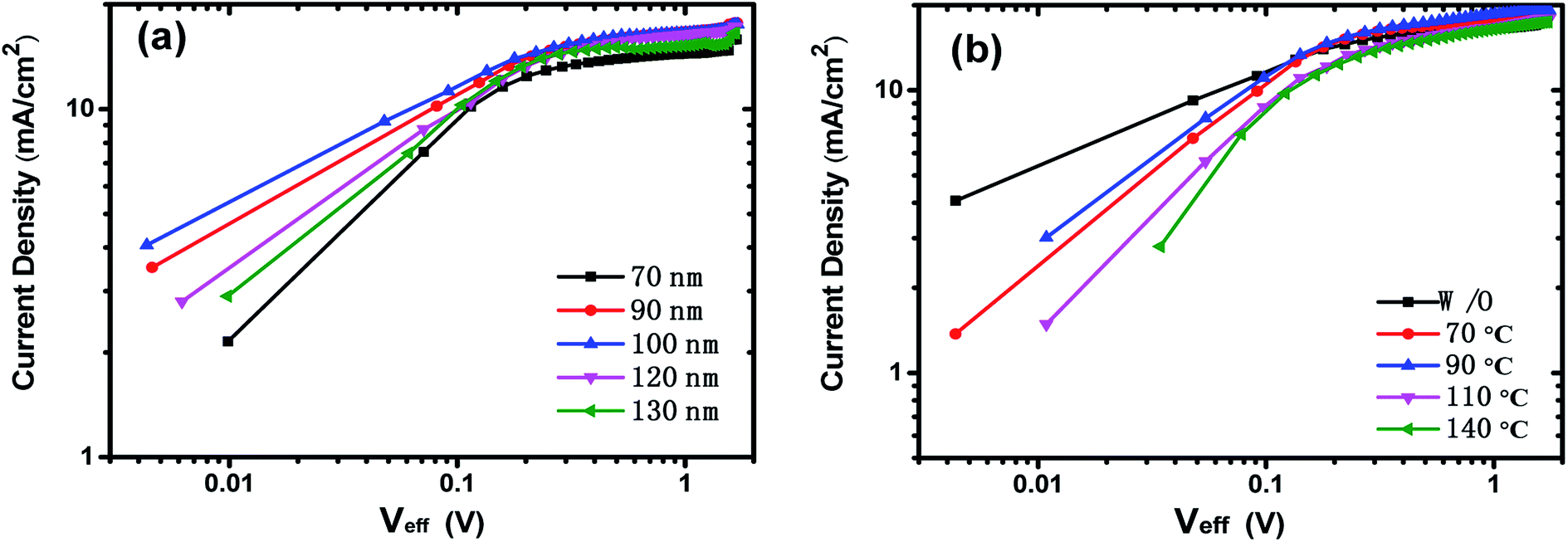 | ||
| Fig. 7 The double-logarithmic plots of the net photocurrent against effective applied voltage of the devices (a) with different films thickness and (b) with different thermal-annealing temperature. | ||
Fig. 7b gives the Jph–Veff curves of the OSCs (with active layer thickness of 100 nm) without and with thermal-annealing at different temperature, and the maximum exciton generation rate Gmax was estimated to be 1.09 × 1027 m−3 s−1, 1.15 × 1027 m−3 s−1, 1.20 × 1027 m−3 s−1, 1.12 × 1027 m−3 s−1 and 1.08 × 1027 m−3 s−1, respectively for the device without thermal-annealing and for the devices with thermal-annealing at 70, 90, 110 and 140 °C. The results indicate that thermal-annealing under appropriate temperature could promote exciton generation rate. Under short circuit conditions, Jsc/Jsat is reported as the product of exciton dissociation efficiency (charge carriers generation) and charge collection efficiency.46 The Jsc/Jsat value is 0.935 for the device without thermal-annealing, and thermal-annealing at 70 °C and 90 °C improve the Jsc/Jsat value to 0.937 and 0.942, respectively. However, higher thermal-annealing temperature would deteriorate the Jsc/Jsat value, and the Jsc/Jsat is 0.909 and 0.908 for the devices with 110 °C and 140 °C thermal-annealing. The optimal Jsc/Jsat value of the device with 90 °C thermal-annealing implies that the improved phase separation of active layer and the reduced roughness of the active layer film surface (Fig. 2c) induced by thermal-annealing at suitable temperature facilitate charge transport in the active layer and charge extraction at the electrode, thus boost the Jsc and improve performance of PTB7:PC71BM organic solar cells.
4. Conclusion
In summary, we prepared PTB7:PC71BM BHJ organic solar cells, and studied the effect of active layer thickness and thermal-annealing treatment on the charge transport and extraction performance detailedly. The thickness of active layer is a basic and important parameter that affects photoelectric performance of organic solar cells. There is an optimized thickness of active layer to balance light absorption and charge transport. Based on the overall photovoltaic performance, 100 nm is the rational thickness of active layer in this study. Thermal-annealing at appropriate temperature could optimize the active layer morphology, and improve the interface contact between active layer and electrode, which provide efficient path for carrier transport in the active layer and collection at the electrode. The TPV/TPC results imply that thermal-annealing could suppress charge recombination, facilitate carrier transport and collection, and the high carrier mobility of the device with 90 °C thermal-annealing was verified by the carrier mobility measurement with Photo-CELIV technique. The optimal PCE was obtained as 8.28% for the device with active layer thickness of 100 nm and treated with 90 °C thermal-annealing. Our results show that active layer thickness optimization and thermal-annealing treatment could improve charge transport and extraction effectively, and enhance photovoltaic performance of PTB7:PC71BM solar cells obviously. When we study organic solar cells with other donor/acceptor system, these facile and effective strategies may be good choice for performance improvement.Conflicts of interest
There are no conflicts to declare.Acknowledgements
This work was supported by National Natural Science Foundation of China (61705003, 11605012); the Construction of service capability of scientific and technological innovation—Fundamental Research Funds (PXM2018_014213_000033) and Scientific Research Ability Promotion Plan of Graduate Student of Beijing Technology and Business University.References
- R. Mishra, R. Regar, V. Singh, P. Panini, R. Singhal, M. L. Keshtov, G. D. Sharmad and J. Sankar, J. Mater. Chem. A, 2012, 1 Search PubMed.
- A. R. Chatri, S. Torabi, V. M. L. Corre and L. J. A. Koster, ACS Appl. Mater. Interfaces, 2018, 10, 12013 CrossRef PubMed.
- D. H. Apaydına, D. E. Yildiz and A. C. L. Toppare, Sol. Energy Mater. Sol. Cells, 2013, 113, 100 CrossRef.
- T. S. Li, L. Ye, W. C. Zhao, H. P. Yan, B. Yang, D. L. Liu, W. N. Li, H. Ade and J. H. Hou, J. Am. Chem. Soc., 2018, 140, 7159 CrossRef PubMed.
- L. X. Meng, Y. M. Zhang, X. G. Wan, C. X. Li, X. Zhang, Y. B. Wang, X. Ke, Z. Xiao, L. M. Ding, R. X. Xia, H.-L. Yip, Y. Cao and Y. S. Chen, Science, 2018, 361, 1094 CrossRef CAS PubMed.
- X. L. Ma, M. Luo, W. Gao, J. Yuan, Q. S. An, M. Zhang, Z. H. Hu, J. H. Gao, J. X. Wang, Y. P. Zou, C. L Yang and F. J. Zhang, J. Mater. Chem. A, 2019, 7, 7843 RSC.
- G. Yu, J. Gao, J. C. Hummelen, F. Wudl and A. J. Heeger, Science, 1995, 270, 1789 CrossRef CAS.
- M. C. Scharber and N. S. Sariciftci, Prog. Polym. Sci., 2013, 38, 1929 CrossRef CAS PubMed.
- F. W. Zhao, S. X. Dai, Y. Wu, Q. Q. Zhang, J. Y. Wang, L. Jiang, Q. D. Ling, Z. X. Wei, W. Ma, W. You, C. R. Wang and X. W. Zhan, Adv. Mater., 2017, 29, 1700144 CrossRef PubMed.
- W. Li, Z. Y. Liu, R. J. Yang, Q. Guan, W. G. Jiang, A. Islam, T. Lei, L. Hong, R. X. Peng and Z. Y. Ge, ACS Appl. Mater. Interfaces, 2017, 9, 27083 CrossRef CAS PubMed.
- P. Friederich, V. Meded, A. Poschlad, T. Neumann, V. Rodin, V. Stehr, F. Symalla, D. Danilov, G. Lüdemann, R. F. Fink, I. Kondov, F. V. Wrochem and W. Wenzel, Adv. Funct. Mater., 2016, 26, 5757 CrossRef CAS.
- G. P. Luo, X. G. Ren, S. Zhang, H. B. Wu, W. C. H. Choy, Z. C. He and Y. Cao, Small, 2016, 12, 1547 CrossRef CAS PubMed.
- T. Kirchartz, T. Agostinelli, M. Campoy-Quiles, W. Gong and J. Nelson, J. Phys. Chem. Lett., 2012, 3, 3471 Search PubMed.
- C. H. To, A. Ng, Q. Dong, A. B. Djurišić, J. A. Zapien, W. K. Chan and C. Surya, ACS Appl. Mater. Interfaces, 2015, 7, 13198 CrossRef CAS PubMed.
- G. Li, Y. Yao, H. Yang, V. Shrotriya, G. E. Yang and Y. Yang, Adv. Funct. Mater., 2007, 17, 1636 CrossRef CAS.
- L. Ciammaruchi, F. Brunetti and I. Visoly-Fisher, Sol. Energy, 2016, 137, 490 CrossRef CAS.
- D. H. Wang and A. K. K. Kyaw, Appl. Phys. Lett., 2014, 105, 103301 CrossRef.
- X. X. Zhu, F. J. Zhang, Q. S. An, H. Huang, Q. Q. Sun, L. L. Li, F. Teng and W. H. Tang, Sol. Energy Mater. Sol. Cells, 2015, 132, 528 CrossRef CAS.
- Y.-Y. Lai, P.-I. Shih, Y.-P. Li, C.-E. Tsai, J.-S. Wu, Y.-J. Cheng and C.-S. Hsu, ACS Appl. Mater. Interfaces, 2013, 5, 5122 CrossRef CAS PubMed.
- K. Borse, R. Sharma, H. P. Sagar, P. A. Reddy, D. Gupta and A. Yella, Org. Electron., 2017, 41, 280 CrossRef CAS.
- H. Jin, J. Olkkonen, M. Tuomikoski, P. Kopola, A. Maaninen and J. Hast, Sol. Energy Mater. Sol. Cells, 2010, 94, 465 CrossRef CAS.
- G. H. Zhao, X. F. Qiao, B. B. Chen and B. Hu, Org. Electron., 2013, 14, 2192 CrossRef.
- G. C. Zhang, K. Zhang, Q. W. Yin, X. F. Jiang, Z. Y. Wang, J. M. Xin, W. Ma, H. Yan, F. Huang and Y. Cao, J. Am. Chem. Soc., 2017, 139, 2387 CrossRef CAS PubMed.
- Z. C. He, C. M. Zhong, S. J. Su, M. Xu, H. B. Wu and Y. Cao, Nat. Photonics, 2012, 6, 591 CrossRef.
- S. J. Lou, J. M. Szarko, T. Xu, L. P. Yu, T. J. Marks and L. X. Chen, J. Am. Chem. Soc., 2011, 133, 20661 CrossRef CAS PubMed.
- C. H. To, A. Ng, Q. Dong, A. B. Djurišić, J. A. Zapien, W. K. Chan and C. Surya, ACS Appl. Mater. Interfaces, 2015, 7, 13198 CrossRef CAS PubMed.
- W. Kim, J. K. Kim, E. Kim, T. K. Ahn, D. H. Wang and J. H. Park, J. Phys. Chem. C, 2015, 119, 5954 CrossRef CAS.
- L. Wang, S. L. Zhao, Z. Xu, J. Zhao, D. Huang and L. Zhao, Materials, 2016, 9, 171 CrossRef PubMed.
- H.-Y. Chen, S. H. Lin, J. Y. Sun, C.-H. Hsu, S. La and C.-F. Lin, Nanotechnology, 2013, 24, 484009 CrossRef PubMed.
- S. Alem, T. Chu, S. C. Tse, S. Wakim, J. Lu, R. Movileanu, Y. Tao, F. Bélanger, D. Désilets, S. Beaupré, M. Leclerc, S. Rodman, D. Waller and R. Gaudiana, Org. Electron., 2011, 12, 1788 CrossRef CAS.
- G. J. Wang, T. G. Jiu, G. Tang, J. Li, P. D. Li, X. J. Song, F. S. Lu and J. F. Fang, ACS Sustainable Chem. Eng., 2014, 2, 1331 CrossRef CAS.
- L. Y. Lu and T. Xu, J. Phys. Chem. C, 2014, 118, 22834 CrossRef CAS.
- B. Guo, W. B. Li, X. Guo, X. Y. Meng, W. Ma, M. J. Zhang and Y. F. Li, Adv. Mater., 2017, 29, 1712291 Search PubMed.
- Y. F. Zheng, T. Goh, P. Fan, W. Shi, J. S. Yu and A. Taylo, ACS Appl. Mater. Interfaces, 2016, 8, 15724 CrossRef CAS PubMed.
- D. Huang, Y. Li, Z. Xu, S. L. Zhao, L. Zhao and J. Zhao, Phys. Chem. Chem. Phys., 2015, 17, 8053 RSC.
- A.-I. Maher, A. Oliver, S. Steffi and G. Gerhard, Appl. Phys. Lett., 2005, 86, 201120 CrossRef.
- B. Qi and J. Wang, Phys. Chem. Chem. Phys., 2013, 15, 8972–8982 RSC.
- C. M. Proctor and T. Nguyen, Appl. Phys. Lett., 2015, 106, 083301 CrossRef.
- X. H. Li, W. E. I. Sha, W. C. H. Choy, D. D. S. Fung and F. X. Xie, J. Phys. Chem. C, 2012, 116, 7200–7206 CrossRef CAS.
- J. Y. Xiao, Z. M. Chen, G. C. Zhang, Q. Y. Li, Q. W. Yin, X. F. Jiang, F. Huang, Y. X. Xu, H.-L. Yip and Y. Cao, J. Mater. Chem. C, 2018, 6, 4457 RSC.
- P. W. M. Blom, V. D. Mihailetchi, L. J. A. Koster and D. E. Markov, Adv. Mater., 2007, 19, 1551 CrossRef CAS.
- Z. Li, F. Gao, N. C. Greenham and C. R. McNeill, Adv. Funct. Mater., 2011, 21, 1419–1431 CrossRef CAS.
- C. Soci, D. Moses, Q.-H. Xu and A. J. Heeger, Phys. Rev. B: Condens. Matter Mater. Phys., 2005, 72, 245204 CrossRef.
- M. Stephen, K. Genevičius, G. Juška, K. Arlauskas and R. C. Hiorns, Polym. Int., 2017, 66, 13 CrossRef CAS.
- M. Neukom, S. Züfle, S. Jenatsch and B. Ruhstaller, Sci. Technol. Adv. Mater., 2018, 19, 292 CrossRef PubMed.
- L. Y. Lu and L. P. Yu, Adv. Mater., 2014, 26, 4413 CrossRef CAS PubMed.
| This journal is © The Royal Society of Chemistry 2019 |